JP6987871B2 - Manufacturing method of sealed optical semiconductor device - Google Patents
Manufacturing method of sealed optical semiconductor device Download PDFInfo
- Publication number
- JP6987871B2 JP6987871B2 JP2019540934A JP2019540934A JP6987871B2 JP 6987871 B2 JP6987871 B2 JP 6987871B2 JP 2019540934 A JP2019540934 A JP 2019540934A JP 2019540934 A JP2019540934 A JP 2019540934A JP 6987871 B2 JP6987871 B2 JP 6987871B2
- Authority
- JP
- Japan
- Prior art keywords
- optical semiconductor
- semiconductor device
- sealing film
- semiconductor element
- film
- Prior art date
- Legal status (The legal status is an assumption and is not a legal conclusion. Google has not performed a legal analysis and makes no representation as to the accuracy of the status listed.)
- Active
Links
Images

Classifications
-
- H—ELECTRICITY
- H01—ELECTRIC ELEMENTS
- H01L—SEMICONDUCTOR DEVICES NOT COVERED BY CLASS H10
- H01L33/00—Semiconductor devices with at least one potential-jump barrier or surface barrier specially adapted for light emission; Processes or apparatus specially adapted for the manufacture or treatment thereof or of parts thereof; Details thereof
- H01L33/48—Semiconductor devices with at least one potential-jump barrier or surface barrier specially adapted for light emission; Processes or apparatus specially adapted for the manufacture or treatment thereof or of parts thereof; Details thereof characterised by the semiconductor body packages
- H01L33/52—Encapsulations
-
- H—ELECTRICITY
- H01—ELECTRIC ELEMENTS
- H01L—SEMICONDUCTOR DEVICES NOT COVERED BY CLASS H10
- H01L33/00—Semiconductor devices with at least one potential-jump barrier or surface barrier specially adapted for light emission; Processes or apparatus specially adapted for the manufacture or treatment thereof or of parts thereof; Details thereof
- H01L33/48—Semiconductor devices with at least one potential-jump barrier or surface barrier specially adapted for light emission; Processes or apparatus specially adapted for the manufacture or treatment thereof or of parts thereof; Details thereof characterised by the semiconductor body packages
- H01L33/50—Wavelength conversion elements
-
- H—ELECTRICITY
- H01—ELECTRIC ELEMENTS
- H01L—SEMICONDUCTOR DEVICES NOT COVERED BY CLASS H10
- H01L33/00—Semiconductor devices with at least one potential-jump barrier or surface barrier specially adapted for light emission; Processes or apparatus specially adapted for the manufacture or treatment thereof or of parts thereof; Details thereof
- H01L33/48—Semiconductor devices with at least one potential-jump barrier or surface barrier specially adapted for light emission; Processes or apparatus specially adapted for the manufacture or treatment thereof or of parts thereof; Details thereof characterised by the semiconductor body packages
- H01L33/52—Encapsulations
- H01L33/54—Encapsulations having a particular shape
-
- H—ELECTRICITY
- H01—ELECTRIC ELEMENTS
- H01L—SEMICONDUCTOR DEVICES NOT COVERED BY CLASS H10
- H01L33/00—Semiconductor devices with at least one potential-jump barrier or surface barrier specially adapted for light emission; Processes or apparatus specially adapted for the manufacture or treatment thereof or of parts thereof; Details thereof
- H01L33/48—Semiconductor devices with at least one potential-jump barrier or surface barrier specially adapted for light emission; Processes or apparatus specially adapted for the manufacture or treatment thereof or of parts thereof; Details thereof characterised by the semiconductor body packages
- H01L33/52—Encapsulations
- H01L33/56—Materials, e.g. epoxy or silicone resin
-
- H—ELECTRICITY
- H01—ELECTRIC ELEMENTS
- H01L—SEMICONDUCTOR DEVICES NOT COVERED BY CLASS H10
- H01L2933/00—Details relating to devices covered by the group H01L33/00 but not provided for in its subgroups
- H01L2933/0008—Processes
- H01L2933/0033—Processes relating to semiconductor body packages
- H01L2933/0041—Processes relating to semiconductor body packages relating to wavelength conversion elements
-
- H—ELECTRICITY
- H01—ELECTRIC ELEMENTS
- H01L—SEMICONDUCTOR DEVICES NOT COVERED BY CLASS H10
- H01L2933/00—Details relating to devices covered by the group H01L33/00 but not provided for in its subgroups
- H01L2933/0008—Processes
- H01L2933/0033—Processes relating to semiconductor body packages
- H01L2933/005—Processes relating to semiconductor body packages relating to encapsulations
Description
本発明は、封止フィルムを用いた封止光半導体デバイスの製造方法に関する。
本願は、2017年9月8日に、日本に出願された特願2017−172928号に基づき優先権を主張し、その内容をここに援用する。The present invention relates to a method for manufacturing a sealed optical semiconductor device using a sealing film.
This application claims priority based on Japanese Patent Application No. 2017-172928 filed in Japan on September 8, 2017, the contents of which are incorporated herein by reference.
フォトカプラー、発光ダイオード、固体撮像素子等の光半導体素子を搭載する光半導体装置において、光半導体素子は、光半導体素子の信頼性を向上させるために封止剤を用いて封止される。光半導体装置を封止する方法としては、封止フィルムを用いて封止する方法が知られている。 In an optical semiconductor device equipped with an optical semiconductor element such as a photocoupler, a light emitting diode, and a solid-state imaging element, the optical semiconductor element is sealed with a sealing agent in order to improve the reliability of the optical semiconductor element. As a method of sealing an optical semiconductor device, a method of sealing using a sealing film is known.
例えば、特許文献1には、少なくとも1つのLED素子を基材上に載置し、第1及び第2の表面を有し、該第1の表面が基材フィルムで支持されたバインダーと、蛍光体粒子とを含む、所定の形状のラミネーション層を前記したLED素子上に配置し、前記ラミネーション層を第1の温度まで加熱し、該ラミネーション層を軟化させ、前記ラミネーション層とLED素子の周囲の基材との間で気密シールを形成し、次いで、前記基材フィルムを取り除いた上で、減圧下でラミネーション層を第2の温度まで加熱して前記ラミネーション層と基材の間の空気を除去し、その後、大気圧下に戻すことにより前記基材に対してラミネーション層をプレスしてLED素子を覆うラミネーション層を形成する、LEDデバイスの製造方法が記載されている。
For example, in
特許文献2には、基材ウエハーの第1の面の内側部分に載置された発光ダイオードアレイ等の物品を所定形状のラミネーション層でコンフォーマルコートする前に、前記したラミネーション層の中央部分を加熱して流動可能な状態にする1回の加熱工程を含む減圧ラミネーション方法であって、前記したラミネーション層の端部と前記第1の面の外側部分とで形成された気密シールと、前記したラミネーション層と、前記した第1の面とで構成された気密された内側領域により、加熱して流動可能な状態となった前記したラミネーション層の中央部分が前記した第1の面の内側部分から離れて配置される工程を含む、減圧ラミネーション方法が記載されている。
In
特許文献3には、光半導体素子を封止するように使用される封止層を備える封止シートであって、前記した封止層を、周波数1Hzおよび昇温速度10℃/分の条件で動的粘弾性測定することにより得られる貯蔵剪断弾性率G’と温度Tとの関係を示す曲線が、極小値を有し、前記した極小値における温度Tが、60℃以上、200℃以下の範囲にあり、前記した極小値における貯蔵剪断弾性率G’が、5Pa以上、1,000Pa以下の範囲にある封止シートを用意するシート用意工程と、基材に配置される光半導体素子を用意する素子用意工程と、前記した封止シートを、60℃以上、200℃以下の温度で、前記した光半導体素子に対して熱プレスする熱プレス工程と、を備えることを特徴とする、封止光半導体素子の製造方法が記載されている。
特許文献4には、光半導体素子に直接的または間接的に貼着するように使用される貼着層を備える貼着シートであって、前記した貼着層を、周波数1Hzおよび昇温速度20℃/分の条件で動的粘弾性測定することにより得られる貯蔵剪断弾性率G’と温度Tとの関係を示す曲線が、極小値を有し、前記した極小値における温度Tが、40℃以上、200℃以下の範囲にあり、前記した極小値における貯蔵剪断弾性率G’が、1,000Pa以上、90,000Pa以下の範囲にある貼着シートを用意するシート用意工程と、基材に配置される光半導体素子を用意する素子用意工程と、前記した貼着シートを、40℃以上、200℃以下の温度で、前記した光半導体素子に対して直接的または間接的に熱プレスする熱プレス工程と、を備えることを特徴とする、貼着光半導体素子の製造方法が記載されている。 Patent Document 4 describes a sticking sheet provided with a sticking layer used for directly or indirectly sticking to an optical semiconductor device, wherein the above-mentioned sticking layer has a frequency of 1 Hz and a temperature rise rate of 20. The curve showing the relationship between the storage shear elasticity G'and the temperature T obtained by dynamic viscoelasticity measurement under the condition of ° C./min has a minimum value, and the temperature T at the above-mentioned minimum value is 40 ° C. As described above, the sheet preparation step of preparing the adhesive sheet in the range of 200 ° C. or lower and the storage shear elasticity G'at the above-mentioned minimum value in the range of 1,000 Pa or more and 90,000 Pa or less, and the base material. The element preparation step of preparing the optical semiconductor element to be arranged and the heat of directly or indirectly heat-pressing the above-mentioned bonding sheet to the above-mentioned optical semiconductor element at a temperature of 40 ° C. or higher and 200 ° C. or lower. A method for manufacturing a bonded optical semiconductor device, which comprises a pressing process, is described.
しかしながら、封止フィルムを用いて、より簡便に光半導体素子を封止することができる、封止光半導体デバイスの製造方法が望まれている。 However, there is a demand for a method for manufacturing a sealed optical semiconductor device, which can more easily seal an optical semiconductor element by using a sealing film.
本発明の目的は、封止フィルムを用いて簡便に且つ高い信頼性で光半導体素子を封止できる、封止光半導体デバイスの製造方法を提供することにある。 An object of the present invention is to provide a method for manufacturing a sealed optical semiconductor device capable of easily and highly reliablely sealing an optical semiconductor element using a sealing film.
本発明者は、上述した課題を解決するために鋭意検討し、封止フィルムを用いて光半導体素子を封止する場合に、特定の温度条件でラミネート工程を行うことにより、簡便且つ高い信頼性で基板上に搭載された光半導体素子を封止できることを見出し、本発明を完成させた。 The present inventor has diligently studied in order to solve the above-mentioned problems, and when sealing an optical semiconductor device using a sealing film, by performing a laminating step under specific temperature conditions, it is easy and highly reliable. We found that the optical semiconductor element mounted on the substrate can be sealed, and completed the present invention.
本発明の封止光半導体デバイスの製造方法は、
減圧チャンバー内で光半導体素子を搭載する光半導体素子搭載基板上に封止フィルムを載置し、前記減圧チャンバー内を減圧する工程、
前記封止フィルムを加熱して、前記封止フィルムの少なくとも周辺部を前記光半導体素子搭載基板の表面に熱融着させる工程、
前記減圧チャンバー内の減圧を解除して、前記封止フィルムで前記光半導体素子搭載基板を封止する工程を含み、
前記減圧チャンバー内の減圧を解除する時点の前記光半導体素子搭載基板の温度T2が、前記封止フィルムが0.02〜0.15MPaの引張強度及び150〜450%の破断伸度を示す温度であることを特徴にする。The method for manufacturing a sealed optical semiconductor device of the present invention is as follows.
A step of placing a sealing film on a substrate on which an optical semiconductor element is mounted in a decompression chamber and depressurizing the inside of the decompression chamber.
A step of heating the sealing film to heat-sealing at least a peripheral portion of the sealing film to the surface of the substrate on which the optical semiconductor device is mounted.
The step of releasing the depressurization in the decompression chamber and sealing the substrate on which the optical semiconductor element is mounted with the sealing film is included.
The temperature T 2 of the optical semiconductor element mounting board at the time of releasing the vacuum in the vacuum chamber is, the temperature at which the sealing film exhibits an elongation at break of the tensile strength and 150-450% of 0.02~0.15MPa It is characterized by being.
本発明の封止光半導体デバイスの製造方法において、封止フィルムが、熱硬化性シリコーン樹脂で構成されることが好ましい。 In the method for manufacturing a sealed optical semiconductor device of the present invention, it is preferable that the sealing film is composed of a thermosetting silicone resin.
本発明の封止光半導体デバイスの製造方法において、封止フィルムが蛍光体を含有する場合、前記の封止フィルム中に90質量%以下の蛍光体を含むことが好ましい。 In the method for producing a sealed optical semiconductor device of the present invention, when the sealing film contains a fluorescent substance, it is preferable that the sealing film contains 90% by mass or less of the fluorescent substance.
本発明の封止光半導体デバイスの製造方法において、封止フィルムが、10μm以上300μm以下の厚さを有することが好ましい。 In the method for manufacturing a sealed optical semiconductor device of the present invention, it is preferable that the sealing film has a thickness of 10 μm or more and 300 μm or less.
本発明の封止光半導体デバイスの製造方法において、温度T2が、70℃以上180℃以下であることが好ましい。In the method for manufacturing a sealed optical semiconductor device of the present invention, the temperature T 2 is preferably 70 ° C. or higher and 180 ° C. or lower.
本発明の封止光半導体デバイスの製造方法において、光半導体素子間の最小距離が、封止フィルムの厚さよりも長いことが好ましい。 In the method for manufacturing a sealed optical semiconductor device of the present invention, it is preferable that the minimum distance between optical semiconductor elements is longer than the thickness of the sealing film.
本発明の封止光半導体デバイスの製造方法において、光半導体素子の高さTと、光半導体素子間の距離Lとのアスペクト比(T/L)が、最大で3以下であることが好ましい。 In the method for manufacturing a sealed optical semiconductor device of the present invention, the aspect ratio (T / L) between the height T of the optical semiconductor element and the distance L between the optical semiconductor elements is preferably 3 or less at the maximum.
本発明の封止光半導体デバイスの製造方法は、簡便且つ高い信頼性で封止光半導体デバイスを製造できるという特徴がある。 The method for manufacturing a sealed optical semiconductor device of the present invention is characterized in that it can manufacture a sealed optical semiconductor device easily and with high reliability.
以下、本発明の実施の形態について詳細に説明する。本発明は以下の実施の形態に限定されるものではなく、その要旨の範囲内で種々変形して実施することができる。 Hereinafter, embodiments of the present invention will be described in detail. The present invention is not limited to the following embodiments, and can be variously modified and implemented within the scope of the gist thereof.
[封止光半導体デバイスの製造方法]
本発明に係る封止光半導体デバイスの製造方法は、
(1) 減圧チャンバー内で光半導体素子を搭載する光半導体素子搭載基板上に封止フィルムを載置して、前記減圧チャンバー内を減圧する工程、
(2) 前記封止フィルムを加熱して、前記封止フィルムの少なくとも周辺部を前記光半導体素子搭載基板の表面に熱融着させる工程、及び、
(3) 前記減圧チャンバー内の減圧を解除して、前記封止フィルムで前記光半導体素子搭載基板を封止する工程を含み、
前記減圧チャンバー内の減圧を解除する時点の前記光半導体素子搭載基板の温度T2が、前記封止フィルムが0.02〜0.15MPaの引張強度及び150〜450%の破断伸度を示す温度であることに特徴がある。[Manufacturing method of sealed optical semiconductor device]
The method for manufacturing a sealed optical semiconductor device according to the present invention is as follows.
(1) A step of placing a sealing film on a substrate on which an optical semiconductor element is mounted in a decompression chamber to depressurize the inside of the decompression chamber.
(2) A step of heating the sealing film to heat-sealing at least a peripheral portion of the sealing film to the surface of the optical semiconductor device mounting substrate, and
(3) The step of releasing the depressurization in the decompression chamber and sealing the substrate on which the optical semiconductor element is mounted with the sealing film is included.
The temperature T 2 of the optical semiconductor element mounting board at the time of releasing the vacuum in the vacuum chamber is, the temperature at which the sealing film exhibits an elongation at break of the tensile strength and 150 to 450% of 0.02~0.15MPa It is characteristic that it is.
こうした本発明によれば、減圧下で封止フィルムを加熱して封止フィルムの周辺部を光半導体素子搭載基板の表面に熱融着させる工程により、封止フィルムと光半導体素子搭載基板の封止される領域の表面の間に気密空間を形成する工程と、減圧を解除して封止フィルムにより光半導体素子搭載基板を封止する工程とを一連した操作で行うことができるので、簡便に封止光半導体デバイスを製造できる。また、減圧チャンバー内の減圧を解除する時点の光半導体素子搭載基板の温度T2が、封止フィルムが光半導体素子の形状に沿って光半導体素子を被覆する(以下、「コンフォーマルラミネーション」とも言う)ことが可能な力学的物性を示す温度に設定されているので、高い信頼性で光半導体デバイスを封止できる。以下、各工程について詳細に説明する。According to the present invention, the sealing film and the optical semiconductor device mounting substrate are sealed by a step of heating the sealing film under reduced pressure to heat-sealing the peripheral portion of the sealing film to the surface of the optical semiconductor device mounting substrate. Since the step of forming an airtight space between the surfaces of the areas to be stopped and the step of releasing the reduced pressure and sealing the substrate on which the optical semiconductor device is mounted with the sealing film can be performed by a series of operations, it is easy to perform. Encapsulation optical semiconductor devices can be manufactured. Further, the temperature T 2 of the substrate on which the optical semiconductor device is mounted at the time of releasing the depressurization in the decompression chamber causes the sealing film to cover the optical semiconductor element along the shape of the optical semiconductor element (hereinafter, also referred to as “conformal lamination”). Since the temperature is set to show the possible mechanical properties, the optical semiconductor device can be sealed with high reliability. Hereinafter, each step will be described in detail.
(1) 減圧チャンバー内で光半導体素子を搭載する光半導体素子搭載基板上に封止フィルムを載置して、減圧チャンバー内を減圧する工程は、減圧チャンバー内に封止対象である光半導体素子を搭載する光半導体素子搭載基板上に封止フィルムを配置した後、減圧チャンバー内を減圧する工程である。封止フィルムは封止対象である光半導体素子を封止するのに適した位置で光半導体素子搭載基板上に載置される。 (1) In the step of placing a sealing film on a substrate on which an optical semiconductor element is mounted in the decompression chamber and depressurizing the inside of the decompression chamber, the opto-semiconductor element to be sealed in the decompression chamber is performed. This is a step of depressurizing the inside of the decompression chamber after arranging the sealing film on the substrate on which the optical semiconductor device is mounted. The encapsulating film is placed on the optical semiconductor element mounting substrate at a position suitable for encapsulating the optical semiconductor element to be sealed.
減圧チャンバーは、光半導体素子搭載基板及び封止フィルムを加熱する加熱手段を内部に備える。好ましくは、減圧チャンバーは、加熱手段として、光半導体素子搭載基板及び封止フィルムを加熱するための熱板を内部に備える。こうした減圧チャンバーとしては、例えば、真空ラミネート装置が例示される。工程の安定上、減圧チャンバーは、内部の減圧が完了する前に封止フィルムの周辺部が光半導体素子搭載基板に熱融着することを防ぐために、好ましくは、内部の減圧が完了するまで光半導体素子搭載基板と加熱手段とが接触するのを防ぐための機構を備える。こうした減圧チャンバーとしては、特に限定されないが、例えば、リフトピン昇降機構を有する真空ラミネータが挙げられる。また、専用のラミネーション治具を用いることにより、ダイアフラム型真空ラミネータを用いることもできる。例えば、ラミネーション治具は、スプリング等の弾性体で光半導体素子搭載基板を支える構造を有しており、ダイアフラムゴム膜が定常位置にある場合は、光半導体素子搭載基板を加熱手段から離しておくことができ、ダイアフラムゴム膜に圧力がかかった場合、ラミネーション治具に備えられた弾性体を押圧して光半導体素子搭載基板を加熱手段に接することができるように設計される。また、ラミネーション治具は、ダイアフラムゴム膜がラミネーション治具を押圧する場合であっても、ダイアフラムゴム膜が光半導体素子搭載基板及び封止フィルムに直接接しないように、光半導体素子搭載基板及び封止フィルムを保護する構造を有する。 The decompression chamber is internally provided with a heating means for heating the substrate on which the optical semiconductor element is mounted and the sealing film. Preferably, the decompression chamber is provided with a heating plate for heating the optical semiconductor device mounting substrate and the sealing film as heating means. Examples of such a decompression chamber include a vacuum laminating device. For the stability of the process, the decompression chamber is preferably lighted until the internal depressurization is completed in order to prevent the peripheral portion of the sealing film from being heat-sealed to the substrate on which the optical semiconductor device is mounted before the internal depressurization is completed. It is provided with a mechanism for preventing contact between the semiconductor element mounting substrate and the heating means. Such a decompression chamber is not particularly limited, and examples thereof include a vacuum laminator having a lift pin elevating mechanism. Further, a diaphragm type vacuum laminator can also be used by using a dedicated lamination jig. For example, the lamination jig has a structure in which an elastic body such as a spring supports the optical semiconductor element mounting substrate, and when the diaphragm rubber film is in a stationary position, the optical semiconductor element mounting substrate is separated from the heating means. It is designed so that when pressure is applied to the diaphragm rubber film, the elastic body provided in the lamination jig can be pressed so that the substrate on which the optical semiconductor element is mounted can come into contact with the heating means. Further, the lamination jig has an optical semiconductor element mounting substrate and a seal so that the diaphragm rubber film does not come into direct contact with the optical semiconductor element mounting substrate and the sealing film even when the diaphragm rubber film presses the lamination jig. It has a structure that protects the waterproof film.
光半導体素子は、特に限定されないが、例えば、発光ダイオード(LED)、半導体レーザ、フォトダイオード、フォトトランジスタ、固体撮像、フォトカプラー用発光体と受光体が例示され、特に、発光ダイオード(LED)であることが好ましい。 The optical semiconductor element is not particularly limited, and examples thereof include a light emitting diode (LED), a semiconductor laser, a photodiode, a phototransistor, a solid-state imaging device, a light emitting body for a photocoupler, and a light receiving body, and in particular, a light emitting diode (LED). It is preferable to have.
光半導体素子搭載基板は、光半導体素子を搭載又は実装している基板である。こうした基板としては、光透過率が高いか、反射率の高い材料が好ましい。光半導体素子搭載する基板としては、例えば、銀、金、および銅等の導電性金属;アルミニウム、およびニッケル等の非導電性の金属;PPA、およびLCP等の白色顔料を混合した熱可塑性樹脂;エポキシ樹脂、BT樹脂、ポリイミド樹脂、およびシリコーン樹脂等の白色顔料を含有する熱硬化性樹脂;アルミナ、および窒化アルミナ等のセラミックス等が挙げられる。 The optical semiconductor device mounting substrate is a substrate on which or mounting an optical semiconductor element. As such a substrate, a material having high light transmittance or high reflectance is preferable. As the substrate on which the optical semiconductor element is mounted, for example, conductive metals such as silver, gold, and copper; non-conductive metals such as aluminum and nickel; thermoplastic resins mixed with white pigments such as PPA and LCP; Thermocurable resins containing white pigments such as epoxy resins, BT resins, polyimide resins, and silicone resins; and ceramics such as alumina and alumina nitride.
封止フィルムは、封止対象である光半導体素子を封止するためのものであり、封止剤をフィルム形状に加工したものである。封止フィルムは単独で用いてもよいし、2枚以上で用いてもよい。2枚以上の封止フィルムを用いる場合、同じ種類の封止フィルムを2枚以上用いてもよいし、異なる種類の封止フィルムを組み合わせて用いてもよい。 The encapsulating film is for encapsulating the optical semiconductor element to be encapsulated, and the encapsulant is processed into a film shape. The sealing film may be used alone or in two or more sheets. When two or more sealing films are used, two or more sealing films of the same type may be used, or different types of sealing films may be used in combination.
封止フィルムを構成する封止剤は、熱可塑性材料又は熱硬化性材料で構成され得る。こうした材料としては、有機ポリマー又はシリコーンであり得る。有機ポリマーとしては、熱可塑性樹脂又は熱硬化性樹脂、例えば、ポリオレフィン樹脂、エチルビニルアセテート(EVA)樹脂、エポキシ樹脂、ポリアクリレート樹脂、又はポリ(ビニルブチラール)樹脂が挙げられる。シリコーンとしては、熱可塑性シリコーン又は熱硬化性シリコーンが挙げられ、例えば、ホットメルトシリコーン又は線状シリコーン(又は「直鎖状シリコーン」)が挙げられる。シリコーンはまた、縮合反応、ヒドロシリル化反応、又はフリーラジカル反応により硬化され得る。ある実施形態によれば、封止フィルムは、熱可塑性樹脂で構成され得る。別の実施形態によれば、封止フィルムは、熱硬化性樹脂で構成され得る。さらに別の実施形態によれば、封止フィルムは、熱硬化性シリコーン樹脂で構成され得る。封止フィルムとしては、例えば、国際公開第2016/065016号により開示されているものを使用することができる。このような封止フィルムとしては、東レ・ダウコーニング株式会社製の商品名LF−1200やLF−1201として入手可能である。 The encapsulant constituting the encapsulant film may be composed of a thermoplastic material or a thermosetting material. Such materials may be organic polymers or silicones. Examples of the organic polymer include a thermoplastic resin or a thermosetting resin, for example, a polyolefin resin, an ethyl vinyl acetate (EVA) resin, an epoxy resin, a polyacrylate resin, or a poly (vinyl butyral) resin. Examples of the silicone include thermoplastic silicones and thermosetting silicones, and examples thereof include hot melt silicones and linear silicones (or "linear silicones"). Silicone can also be cured by a condensation reaction, a hydrosilylation reaction, or a free radical reaction. According to certain embodiments, the encapsulating film may be composed of a thermoplastic resin. According to another embodiment, the sealing film may be composed of a thermosetting resin. According to yet another embodiment, the encapsulating film may be composed of a thermosetting silicone resin. As the sealing film, for example, those disclosed in International Publication No. 2016/0605016 can be used. As such a sealing film, it is available under the trade names LF-1200 and LF-1201 manufactured by Toray Dow Corning Co., Ltd.
封止フィルムは、透明性を有する封止フィルムとして使用することもできるが、蛍光体を含有してもよい。蛍光体としては、特に限定されないが、例えば、発光ダイオード(LED)に広く利用されている、酸化物系蛍光体、酸窒化物系蛍光体、窒化物系蛍光体、硫化物系蛍光体、酸硫化物系蛍光体等からなる黄色、赤色、緑色、青色発光蛍光体が挙げられる。酸化物系蛍光体としては、セリウムイオンを包含するイットリウム、アルミニウム、ガーネット系のYAG系緑色〜黄色発光蛍光体、セリウムイオンを包含するテルビウム、アルミニウム、ガーネット系のTAG系黄色発光蛍光体、および、セリウムやユーロピウムイオンを包含するシリケート系緑色〜黄色発光蛍光体が例示される。酸窒化物系蛍光体としては、ユーロピウムイオンを包含するケイ素、アルミニウム、酸素、窒素系のサイアロン系赤色〜緑色発光蛍光体が例示される。窒化物系蛍光体としては、ユーロピウムイオンを包含するカルシウム、ストロンチウム、アルミニウム、ケイ素、窒素系のカズン系赤色発光蛍光体が例示される。硫化物系蛍光体としては、銅イオンやアルミニウムイオンを包含するZnS系緑色発色蛍光体が例示される。酸硫化物系蛍光体としては、ユーロピウムイオンを包含するY2O2S系赤色発光蛍光体が例示される。これらの蛍光体は、1種または2種以上の混合物を用いてもよい。The sealing film can be used as a transparent sealing film, but may contain a fluorescent substance. The phosphor is not particularly limited, but is, for example, an oxide-based phosphor, an oxynitride-based phosphor, a nitride-based phosphor, a sulfide-based phosphor, or an acid widely used for light emitting diodes (LEDs). Examples thereof include yellow, red, green, and blue light emitting phosphors composed of sulfide-based phosphors and the like. Examples of the oxide-based phosphor include yttrium, aluminum, and garnet-based YAG-based green to yellow-emitting phosphors containing cerium ions, terbium, aluminum, and garnet-based TAG-based yellow-emitting phosphors containing cerium ions. Examples thereof include silicate-based green to yellow luminescent fluorophores containing cerium and europium ions. Examples of the oxynitride-based phosphor include silicon, aluminum, oxygen, and nitrogen-based sialone-based red to green luminescent phosphors containing europium ions. Examples of the nitride-based phosphor include calcium, strontium, aluminum, silicon, and nitrogen-based cousin-based red-emitting phosphors containing europium ions. Examples of the sulfide-based phosphor include a ZnS-based green color-developing phosphor containing copper ions and aluminum ions. The oxysulfide phosphor include
蛍光体の平均粒子径は、限定されないが、通常1μm以上、好ましくは5μm以上で、50μm以下、好ましくは20μm以下の範囲内である。平均粒子径は、例えば、レーザー回折散乱式粒度分布測定法で体積累積平均粒子径(D50)を測定することにより測定できる。The average particle size of the phosphor is not limited, but is usually 1 μm or more, preferably 5 μm or more, and 50 μm or less, preferably 20 μm or less. The average particle size can be measured, for example, by measuring the volume cumulative average particle size (D 50 ) by a laser diffraction / scattering type particle size distribution measuring method.
蛍光体の含有量は、特に限定されないが、封止フィルム中に通常90質量%以下の量である。一方、その含有量の下限は限定されず、好ましくは、50質量%以上、より好ましくは60質量%以上の量である。 The content of the phosphor is not particularly limited, but is usually 90% by mass or less in the sealing film. On the other hand, the lower limit of the content is not limited, and is preferably 50% by mass or more, more preferably 60% by mass or more.
封止フィルムは、その他任意成分として、沈降シリカないし湿式シリカ、ヒュームドシリカのような補強性充填剤、これらの充填剤をオルガノハロシラン、オルガノアルコキシシラン、ヘキサオルガノジシラザン等の有機ケイ素化合物により疎水化処理したもの、アルミナ、焼成シリカ、酸化チタン、ガラス、石英、アルミノケイ酸、酸化鉄、酸化亜鉛、炭酸カルシウム、炭化ケイ素、窒化ケイ素、窒化ホウ素等の無機質増量充填剤;シリコーン樹脂、エポキシ樹脂、フッ素樹脂等の有機樹脂微粉末、染料、顔料、難燃剤、耐熱剤等を配合することができる。 The encapsulating film may contain, as other optional components, a reinforcing filler such as precipitated silica or wet silica, fumed silica, or an organic silicon compound such as organohalosilane, organoalkoxysilane, or hexaorganodisilazane. Hydrophobized products, alumina, calcined silica, titanium oxide, glass, quartz, aluminosilicate, iron oxide, zinc oxide, calcium carbonate, silicon carbide, silicon nitride, boron nitride and other inorganic bulking fillers; silicone resin, epoxy resin , Organic resin fine powder such as fluororesin, dye, pigment, flame retardant, heat resistant agent and the like can be blended.
封止フィルムの厚さは、特に限定されないが、例えば、10μm以上、好ましくは20μm以上で、300μm以下、好ましくは200μm以下である。 The thickness of the sealing film is not particularly limited, but is, for example, 10 μm or more, preferably 20 μm or more, 300 μm or less, and preferably 200 μm or less.
光半導体素子搭載基板において、光半導体素子は1つ実装されていてもよいし、2つ以上の複数で実装されていてもよい。好ましくは、光半導体素子搭載基板は複数の光半導体素子を搭載している。光半導体素子搭載基板が複数の光半導体素子を搭載している場合、光半導体素子間の最小距離は、封止フィルムによる光半導体素子の形状に沿った被覆、すなわち、コンフォーマルラミネーションの形成を確保するために、封止フィルムの厚さよりも長いことが好ましい。そのため、光半導体素子間の最小距離は、通常10μm以上であり、好ましくは20μm以上である。また、光半導体素子間の最大距離は、特に限定されないが、通常、封止フィルムの厚さの2倍よりも短い。そのため、光半導体素子間の最大距離は、通常600μm以下であり、好ましくは400μm以下である。また、コンフォーマルラミネーションの形成を確保するために、光半導体素子の頂面から光半導体素子搭載基板の表面までの距離、すなわち、光半導体素子の高さTと、光半導体素子間の距離Lとのアスペクト比(T/L)は、好ましくは最大で3以下であり、より好ましくは最大で2.5以下、さらに好ましくは最大で2以下となるように設計される。 In the optical semiconductor element mounting substrate, one optical semiconductor element may be mounted, or two or more optical semiconductor elements may be mounted. Preferably, the optical semiconductor element mounting substrate mounts a plurality of optical semiconductor elements. When the substrate on which the optical semiconductor element is mounted mounts a plurality of optical semiconductor elements, the minimum distance between the optical semiconductor elements ensures that the encapsulating film covers the optical semiconductor element along the shape, that is, the formation of conformal lamination. Therefore, it is preferably longer than the thickness of the sealing film. Therefore, the minimum distance between the optical semiconductor elements is usually 10 μm or more, preferably 20 μm or more. Further, the maximum distance between the optical semiconductor elements is not particularly limited, but is usually shorter than twice the thickness of the encapsulating film. Therefore, the maximum distance between the optical semiconductor elements is usually 600 μm or less, preferably 400 μm or less. Further, in order to secure the formation of conformal lamination, the distance from the top surface of the optical semiconductor element to the surface of the substrate on which the optical semiconductor element is mounted, that is, the height T of the optical semiconductor element and the distance L between the optical semiconductor elements. The aspect ratio (T / L) of is preferably designed to be 3 or less at the maximum, more preferably 2.5 or less at the maximum, and further preferably 2 or less at the maximum.
減圧チャンバー内の減圧は、従来公知の減圧手段によって行うことができ、例えば、減圧チャンバーの内部と接続された真空ポンプを稼働させることにより行われる。通常、減圧チャンバー内の気圧は300Pa以下、好ましくは、200Pa以下、あるいは133Pa以下まで減圧される。 The depressurization in the decompression chamber can be performed by a conventionally known decompression means, for example, by operating a vacuum pump connected to the inside of the decompression chamber. Normally, the air pressure in the pressure reducing chamber is reduced to 300 Pa or less, preferably 200 Pa or less, or 133 Pa or less.
(2) 封止フィルムを加熱して、封止フィルムの少なくとも周辺部を光半導体素子搭載基板の表面に熱融着させる工程は、封止フィルムを温度T1以上に加熱して、封止フィルムを柔軟にして撓ませることにより封止フィルムと光半導体素子搭載基板を接触させ、封止フィルムの少なくとも周辺部を光半導体素子搭載基板の封止される領域の周辺部に熱融着させて、封止フィルムと光半導体素子搭載基板の封止される領域の表面の間に気密空間を形成する工程である。この工程により、封止フィルムにコンフォーマルラミネーションのための適した柔軟性を付与すると共に、封止フィルムと光半導体素子搭載基板の封止される領域の表面の間の空間を密閉(「シール」とも言う)して気密状態にすることができる。(2) In the step of heating the encapsulating film and heat-sealing at least the peripheral portion of the encapsulating film to the surface of the substrate on which the optical semiconductor element is mounted, the encapsulating film is heated to a temperature T 1 or higher to form the encapsulating film. The encapsulating film and the optical semiconductor device mounting substrate are brought into contact with each other by being flexed and flexed, and at least the peripheral portion of the encapsulating film is heat-sealed to the peripheral portion of the sealed region of the optical semiconductor element mounting substrate. This is a step of forming an airtight space between the surface of the sealing film and the surface of the sealed region of the optical semiconductor device mounting substrate. This process provides the encapsulating film with suitable flexibility for conformal lamination and seals the space between the encapsulating film and the surface of the encapsulated area of the optical semiconductor device mounting substrate (“seal”). It can also be made airtight.
封止フィルムの加熱は、減圧チャンバーに備えられた加熱手段により行われる。例えば、加熱手段としては、減圧チャンバー内に備えられた熱板を利用できる。通常、封止フィルムは、光半導体素子搭載基板を加熱することにより加熱される。例えば、加熱手段として熱板を利用する場合、光半導体素子搭載基板と熱板を接触させることにより、光半導体素子搭載基板より封止フィルムに熱が伝わり、封止フィルムが加熱される。 The encapsulating film is heated by the heating means provided in the decompression chamber. For example, as the heating means, a hot plate provided in the decompression chamber can be used. Usually, the sealing film is heated by heating the substrate on which the optical semiconductor device is mounted. For example, when a hot plate is used as a heating means, heat is transferred from the optical semiconductor element-mounted substrate to the encapsulating film by bringing the optical semiconductor element-mounted substrate into contact with the hot plate, and the encapsulating film is heated.
この工程において、封止フィルムは、温度T1以上の温度であって、温度T2以下の温度に保持される。温度T1は、チャンバー減圧中にフィルムの熱融着が発生して、封止される領域を気密にできない(空気がトラップされて残留する)ほど高温でなければ特に限定されず、高くとも60℃である。また、封止フィルムは、通常、温度T1以上T2以下の温度に1分以上10分以下の間保持される。これは、10分を超えて保持されると、封止フィルムの硬化が進行し、ラミネート不良を起こしやすくなるからである。In this step, the sealing film is maintained at a temperature of T 1 or higher and a temperature of T 2 or lower. The temperature T 1 is not particularly limited unless the temperature is so high that heat fusion of the film occurs during depressurization of the chamber and the sealed region cannot be made airtight (air is trapped and remains), and the
封止フィルムを加熱して、封止フィルムの少なくとも周辺部を光半導体素子搭載基板に熱融着させる工程は、上記(1)工程が完了した後で行われてもよいし、上記(1)工程が完了する前に、上記(1)工程の実行中に行われてもよい。すなわち、減圧チャンバー内の減圧が所定の範囲まで減圧される前に封止フィルムの温度T1以上への加熱を開始してもよい。工程の安定性から、(2)工程は、上記(1)工程の減圧チャンバー内の減圧が完了してから行われることが好ましい。The step of heating the sealing film to heat-sealing at least the peripheral portion of the sealing film to the substrate on which the optical semiconductor device is mounted may be performed after the above-mentioned step (1) is completed, or the above-mentioned (1). It may be performed during the execution of the above step (1) before the step is completed. That is, heating of the sealing film to a temperature T 1 or higher may be started before the depressurization in the decompression chamber is depressurized to a predetermined range. From the viewpoint of the stability of the process, it is preferable that the step (2) is performed after the depressurization in the decompression chamber of the above step (1) is completed.
(3) 減圧チャンバー内の減圧を解除して、封止フィルムで光半導体素子搭載基板を封止する工程は、減圧チャンバー内の減圧を解除して、封止フィルムと光半導体素子搭載基板の封止される領域の表面の間の気密空間と、外気との気圧差により、封止フィルムを光半導体素子搭載基板に対して圧着させ、光半導体素子搭載基板をラミネートする工程である。 (3) In the step of releasing the depressurization in the decompression chamber and sealing the optical semiconductor device mounting substrate with the sealing film, the depressurization in the decompression chamber is released and the sealing film and the optical semiconductor element mounting substrate are sealed. This is a step of crimping the sealing film against the optical semiconductor device mounting substrate by the pressure difference between the airtight space between the surfaces of the stopped region and the outside air, and laminating the optical semiconductor device mounting substrate.
「減圧チャンバー内の減圧を解除する」とは、通常、減圧チャンバーを大気に開放して減圧チャンバー内の減圧を大気圧まで戻すこと意味する。大気圧まで直ぐに戻す必要はなく、封止フィルムを光半導体素子搭載基板に対して圧着させて光半導体素子のコンフォーマルラミネーションを可能にする範囲で徐々に減圧を解除してもよい。通常、減圧チャンバー内の減圧は10kPa/秒の速度、好ましくは、50kPa/秒の速度、あるいは100kPa/秒の速度で大気圧まで戻される。これは、減圧から大気圧までの速度があまりに遅いと、気密のリークが発生し、ラミネーションが十分にできないおそれがあるからである。 "Releasing the decompression in the decompression chamber" usually means opening the decompression chamber to the atmosphere and returning the decompression in the decompression chamber to atmospheric pressure. It is not necessary to immediately return to atmospheric pressure, and the depressurization may be gradually released to the extent that the sealing film is pressure-bonded to the substrate on which the optical semiconductor element is mounted to enable conformal lamination of the optical semiconductor element. Normally, the depressurization in the decompression chamber is returned to atmospheric pressure at a rate of 10 kPa / sec, preferably 50 kPa / sec, or 100 kPa / sec. This is because if the speed from decompression to atmospheric pressure is too slow, an airtight leak may occur and sufficient lamination may not be possible.
減圧チャンバー内の減圧を解除する時点での光半導体素子搭載基板の温度T2は、封止フィルムが光半導体素子のコンフォーマルラミネーションの形成を可能にするのに適した物理的特性を有する温度に設定される。具体的には、温度T2は、封止フィルムが0.02〜0.15MPaの引張強度及び150〜450%の破断伸度を示す温度である。好ましくは、T2は、封止フィルムが0.03MPa以上の引張強度を示す温度である。好ましくは、T2は、封止フィルムが0.12MPa以下の引張強度を示す温度である。また、好ましくは、T2は、封止フィルムが200%以上の破断伸度を示す温度である。好ましくは、T2は、封止フィルムが400%以下の破断伸度を示す温度である。封止フィルムの引張強度及び破断伸度は、本発明の実施前に予め当該技術分野の通常の方法により測定される。例えば、TAインスツルメント社製、RSA−G2動的粘弾性測定機を用いて測定することができる。封止フィルムが温度T2で上記した物理的特性を示すことにより、高い信頼性で基板上に搭載された光半導体素子を封止できる。 The temperature T 2 of the substrate on which the optical semiconductor device is mounted at the time of releasing the depressurization in the decompression chamber is set to a temperature at which the encapsulating film has physical properties suitable for enabling the formation of conformal lamination of the optical semiconductor device. Set. Specifically, the temperature T 2 is a temperature at which the sealing film exhibits a tensile strength of 0.02 to 0.15 MPa and a breaking elongation of 150 to 450%. Preferably, T 2 is a temperature at which the sealing film exhibits a tensile strength of 0.03 MPa or more. Preferably, T 2 is a temperature at which the sealing film exhibits a tensile strength of 0.12 MPa or less. Further, preferably, T 2 is a temperature at which the sealing film exhibits a breaking elongation of 200% or more. Preferably, T 2 is a temperature at which the encapsulating film exhibits a breaking elongation of 400% or less. The tensile strength and breaking elongation of the encapsulating film are measured in advance by ordinary methods in the art prior to the implementation of the present invention. For example, it can be measured using an RSA-G2 dynamic viscoelasticity measuring machine manufactured by TA Instruments. Since the sealing film exhibits the above-mentioned physical characteristics at the temperature T 2 , the optical semiconductor element mounted on the substrate can be sealed with high reliability.
減圧チャンバー内の減圧を解除する時点での光半導体素子搭載基板の温度T2は、上記した条件を満たせば特に限定されないが、例えば、70℃以上、好ましくは90℃以上であり、180℃以下、好ましくは150℃以下である。 The temperature T 2 of the substrate on which the optical semiconductor device is mounted at the time of releasing the decompression in the decompression chamber is not particularly limited as long as the above conditions are satisfied, but is, for example, 70 ° C. or higher, preferably 90 ° C. or higher, and 180 ° C. or lower. It is preferably 150 ° C. or lower.
以下、図面を用いて本願発明の特定の実施形態をより詳細に説明する。 Hereinafter, specific embodiments of the present invention will be described in more detail with reference to the drawings.
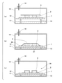
図1は、減圧チャンバーとして、リフトピン昇降機構を有する真空ラミネータ10を用いて実施される本発明に係る製造方法の一例を示す模式的な断面図である。
FIG. 1 is a schematic cross-sectional view showing an example of a manufacturing method according to the present invention, which is carried out by using a
図1(a)は、当該実施形態における本発明の工程(1)を示している。この工程(1)において、光半導体素子2を搭載する光半導体素子搭載基板1上に、封止フィルム3が載置されている。また、光半導体素子搭載基板1は、リフトピン13によって昇降可能な中板12上に配置されている。真空ラミネータ10の内部は、開口14を介して減圧手段(図示せず)と接続しており、減圧手段の働きにより真空ラミネータ10の内部が減圧される。ここで、工程(1)の開始時点では、中板12はリフトピン13によって熱板11から離れて設置されており、真空ラミネータ10内部の減圧が十分に進行する前に熱板11によって封止フィルム3が温度T1以上に加熱されるのを防ぐことができる。このため、工程の安定性が確保できる。FIG. 1A shows the step (1) of the present invention in the embodiment. In this step (1), the sealing
図1(b)は、当該実施形態における本発明の工程(2)を示している。この工程(2)において、リフトピン13を下降させ、中板12を熱板11と接触するように移動させる。その結果、熱板11からの熱が光半導体素子搭載基板1を介して封止フィルム3に伝わり、封止フィルム3が温度T1より高い温度まで加熱される。封止フィルム3が加熱されると、封止フィルム3は柔軟になって変形し、封止フィルム3の周辺部20が光半導体素子搭載基板1の表面と接触し、周辺部20は半導体素子搭載基板1の表面に熱融着される。この時、封止フィルム3と光半導体素子搭載基板1の封止される領域の表面の間に気密空間21が形成される。FIG. 1 (b) shows the step (2) of the present invention in the embodiment. In this step (2), the
図1(c)は、当該実施形態における本発明の工程(3)を示している。この工程(3)において、半導体素子搭載基板1の温度がT2となった時点で、開口14を介して真空ラミネータ10内部の減圧を解除することにより、外気と気密空間21(図1(c)には図示されていない)との気圧差によって封止フィルム3が光半導体素子搭載基板1に対して圧着され、光半導体素子2が封止される。その結果、封止光半導体デバイス30が得られる。工程(3)において、光半導体素子搭載基板1の温度が、封止フィルムが光半導体素子のコンフォーマルラミネーションの形成を可能にするのに適した物理的特性を示す温度である、温度T2となった時点で真空ラミネータ10の内部の減圧を解除することにより、封止フィルム3による光半導体素子2の形状に沿った被覆を高い信頼性で形成できる。FIG. 1 (c) shows the step (3) of the present invention in the embodiment. In this step (3), when the temperature of the semiconductor
図2は、減圧チャンバーとして、ダイアフラム型真空ラミネータ40及びラミネーション治具50を用いて実施される、本発明に係る製造方法の一例を示す模式的な断面図である。
FIG. 2 is a schematic cross-sectional view showing an example of a manufacturing method according to the present invention, which is carried out by using a diaphragm
図2(a)は、当該実施形態における本発明の工程(1)を示している。ダイアフラム型真空ラミネータ40の内部は、ダイアフラムゴム膜41を介して上室42と下室43に分かれており、上室42と下室43の内部は、それぞれの開口15及び16を介して減圧手段(いずれも図示せず)に接続しており、減圧手段の働きにより上室42と下室43の内部が減圧される。なお、上室42の開口15は、加圧手段にも接続されていてもよい。この図では、下室43内で、光半導体素子2を搭載する光半導体素子搭載基板1上に封止フィルム3が載置されている。さらに、光半導体素子搭載基板1は、専用のラミネーション治具50の内部に配置されている。このラミネーション治具50は、スプリング51を備えており、スプリング51により、ラミネーション治具50は熱板11から離れて設置されており、下室43の減圧が十分に進行する前に熱板11によって封止フィルム3が温度T1以上に加熱されるのを防ぐことができる。このため、工程の安定性が確保できる。FIG. 2A shows the step (1) of the present invention in the embodiment. The inside of the diaphragm
図2(b)は、当該実施形態における本発明の工程(2)を示している。この工程(2)において、上室42の減圧を、開口15を介して解除する。これにより、上室42と下室43(図2(b)には図示されていない)の減圧差によりダイアフラムゴム膜41が下室43を押圧するように変形し、スプリング51が押圧されて、ラミネーション治具50が熱板11と接触する。その結果、熱板11からの熱が光半導体素子搭載基板1を介して封止フィルム3に伝わり、封止フィルム3がT1以上の温度まで加熱される。封止フィルム3が温度T1以上に加熱されると、封止フィルム3は柔軟になって変形し、封止フィルム3の周辺部20が光半導体素子搭載基板1の表面と接触する。その結果、周辺部20は半導体素子搭載基板1の表面に熱融着され、封止フィルム3と光半導体素子搭載基板1の封止される領域の表面の間に気密空間21が形成される。この実施形態において、ラミネーション治具50の上枠52の構造により、ダイアフラムゴム膜41が下室43を押圧した場合であっても、ダイアフラムゴム膜41により封止フィルム3が半導体素子搭載基板1に対して押圧されるのを防ぐことができ、その結果、気密空間21の形成を確保できる。FIG. 2B shows the step (2) of the present invention in the embodiment. In this step (2), the depressurization of the
図2(c)は、当該実施形態における本発明の工程(3)を示している。この工程(3)において、半導体素子搭載基板1の温度がT2となった時点で、開口16を介して下室43内部の減圧を解除することにより、外気と気密空間21(図2(c)には図示されていない)との気圧差によって封止フィルム3が光半導体素子搭載基板1に対して圧着され、光半導体素子2が封止される。その結果、封止光半導体デバイス30が得られる。工程(3)において、光半導体素子搭載基板1の温度が、封止フィルム3が光半導体素子2のコンフォーマルラミネーションの形成を可能にするのに適した物理的特性を示す温度である、温度T2となった時点で、下室43の内部の減圧を解除することにより、封止フィルム3による光半導体素子2の形状に沿った被覆を高い信頼性で形成できる。FIG. 2 (c) shows the step (3) of the present invention in the embodiment. In this step (3), when the temperature of the semiconductor
本発明の封止光半導体デバイスの製造方法を実施例および比較例により詳細に説明する。但し本発明は以下の実施例の記載に限定されない。 The method for manufacturing the sealed optical semiconductor device of the present invention will be described in detail with reference to Examples and Comparative Examples. However, the present invention is not limited to the description of the following examples.
[封止フィルム]
熱硬化性シリコーン組成物(東レ・ダウコーニング株式会社製、商品名LF−1200)に対して、75質量%、及び85質量%の量でYAG系黄色発光蛍光体粒子(Intematix社製、商品名NYAG4454−S、平均粒径8μm)を混合し、厚さ100μmの封止フィルムA(蛍光体粒子75質量%含有)、及び封止フィルムB(蛍光体粒子85質量%含有)を調製した。[Encapsulating film]
YAG-based yellow luminescent phosphor particles (manufactured by Intematics, trade name) in an amount of 75% by mass and 85% by mass with respect to the thermosetting silicone composition (manufactured by Toray Dow Corning Co., Ltd., trade name LF-1200). NYAG4454-S (with an average particle size of 8 μm) was mixed to prepare a sealing film A (containing 75% by mass of fluorescent particles) and a sealing film B (containing 85% by mass of fluorescent particles) having a thickness of 100 μm.
同様に、熱硬化性シリコーン組成物(東レ・ダウコーニング株式会社製、商品名LF−1201)に対して、75質量%、及び85質量%の量でYAG系黄色発光蛍光体粒子(Intematix社製、商品名NYAG4454−S、平均粒径8μm)を混合し、厚さ100μmの封止フィルムC(蛍光体粒子75質量%含有)、及び封止フィルムD(蛍光体粒子85質量%含有)を調製した。 Similarly, YAG-based yellow luminescent phosphor particles (manufactured by Intematics) in an amount of 75% by mass and 85% by mass with respect to the thermosetting silicone composition (manufactured by Toray Dow Corning Co., Ltd., trade name LF-1201). , Trade name NYAG4454-S, average particle size 8 μm) to prepare a sealing film C (containing 75% by mass of phosphor particles) and a sealing film D (containing 85% by mass of phosphor particles) having a thickness of 100 μm. did.
封止フィルムA〜Dの90℃、100℃、110℃、120℃、及び/又は130℃での引張強度及び破断伸度を、TAインスツルメント社製、RSA−G2動的粘弾性測定機を用いて測定した。長さ10mm、幅25mmのサイズの測定サンプルを調製し、引張速度を10mm/分として測定した。結果を以下の表1に示す。 RSA-G2 dynamic viscoelasticity measuring machine manufactured by TA Instruments Co., Ltd. for measuring the tensile strength and breaking elongation of sealing films A to D at 90 ° C, 100 ° C, 110 ° C, 120 ° C, and / or 130 ° C. Was measured using. A measurement sample having a length of 10 mm and a width of 25 mm was prepared and measured at a tensile speed of 10 mm / min. The results are shown in Table 1 below.
[光半導体素子搭載基板]
光半導体素子搭載基板として、ガラス基板上に、奥行き1mm、幅1mm、高さ0.15mmの直方体状の光半導体素子を、縦に10個、横に10個配置した光半導体素子搭載基板を用いた。光半導体素子間の距離Lは均等に0.15mmであり、光半導体素子の高さTと光半導体素子間の距離Lとのアスペクト比(T/L)は1であった。[Optical semiconductor device mounting substrate]
As a substrate for mounting an optical semiconductor element, a substrate on which a rectangular parallelepiped optical semiconductor element having a depth of 1 mm, a width of 1 mm, and a height of 0.15 mm is arranged vertically and 10 horizontally is used. board. The distance L between the optical semiconductor elements was uniformly 0.15 mm, and the aspect ratio (T / L) between the height T of the optical semiconductor element and the distance L between the optical semiconductor elements was 1.
[実施例1〜5及び比較例1〜9]
封止フィルムA〜Dを用いて、上記半導体素子搭載基板に対して真空ラミネーションを行った。減圧チャンバーとしては、真空ポンプと接続したリフトピン昇降機構を有する真空ラミネータ(日清紡メカトロニクス社製、商品名PVL−0505Sリフトピン機構付き)を用いた。まず、真空ラミネータ内の熱板から離れた位置に配置されたリフトピン昇降機構により昇降可能な中板上に光半導体素子搭載基板を設置し、その上に封止フィルムA、B、C、又はDを載置した。次いで、真空ポンプを駆動させて真空ラミネータ内を133Paまで減圧させた。次いで、中板を下降させて100℃〜180℃に加熱された熱板に接触させた。その後、封止フィルムを3分〜7分間かけて加熱し、光半導体素子搭載基板の温度が所定の温度T2に達した時点で10秒間かけて減圧を大気圧まで戻して、封止光半導体デバイスを得た。[Examples 1 to 5 and Comparative Examples 1 to 9]
Vacuum lamination was performed on the semiconductor device mounting substrate using the sealing films A to D. As the decompression chamber, a vacuum laminator having a lift pin elevating mechanism connected to a vacuum pump (manufactured by Nisshinbo Mechatronics Co., Ltd., trade name PVL-0505S with a lift pin mechanism) was used. First, an optical semiconductor element mounting substrate is placed on a middle plate that can be raised and lowered by a lift pin raising and lowering mechanism arranged at a position away from the hot plate in the vacuum laminator, and the sealing film A, B, C, or D is placed on the substrate. Was placed. Next, the vacuum pump was driven to reduce the pressure inside the vacuum laminator to 133 Pa. Then, the middle plate was lowered and brought into contact with a hot plate heated to 100 ° C. to 180 ° C. After that, the encapsulating film is heated over 3 to 7 minutes, and when the temperature of the substrate on which the optical semiconductor element is mounted reaches a predetermined temperature T 2 , the reduced pressure is returned to atmospheric pressure over 10 seconds, and the encapsulating optical semiconductor is used. Got the device.
得られた封止半導体デバイスを目視により観察して、ボイド及び/又はクラックの発生の有無を確認した。結果を以下の表1に示す。 The obtained sealed semiconductor device was visually observed to confirm the presence or absence of voids and / or cracks. The results are shown in Table 1 below.

表1から、実施例1〜5の製造方法で製造された封止光半導体デバイスは、ボイド及び/又はクラックの発生を生じることがなく、封止フィルムにより、光半導体素子の形状に沿った被覆が形成されていることが確認された。 From Table 1, the sealed optical semiconductor devices manufactured by the manufacturing methods of Examples 1 to 5 do not generate voids and / or cracks, and are coated with the sealing film along the shape of the optical semiconductor element. Was confirmed to be formed.
本発明の封止光半導体デバイスの製造方法は、発光ダイオード(LED)、半導体レーザ、フォトダイオード、フォトトランジスタ、固体撮像、フォトカプラー用発光体及び受光体等の光半導体素子の封止方法として有用である。 The method for manufacturing a sealed optical semiconductor device of the present invention is useful as a method for sealing an optical semiconductor element such as a light emitting diode (LED), a semiconductor laser, a photodiode, a phototransistor, a solid-state imaging, a light emitter for a photocoupler, and a light receiving body. Is.
1 光半導体素子搭載基板
2 光半導体素子
3 封止フィルム
10 真空ラミネータ
11 熱板
12 中板
13 リフトピン
14〜16 開口
20 封止フィルムの周辺部
21 気密空間
30 封止光半導体デバイス
40 ダイアフラム型真空ラミネータ
41 ダイアフラムゴム膜
42 上室
43 下室
50 ラミネーション治具
51 スプリング
52 上枠1 Optical semiconductor
Claims (7)
前記封止フィルムを加熱して、前記封止フィルムの少なくとも周辺部を前記素子搭載基板の表面に熱融着させる工程、及び
前記減圧チャンバー内の減圧を解除して、前記封止フィルムで前記光半導体素子搭載基板を封止する工程を含む、封止光半導体デバイスの製造方法であって、
前記減圧チャンバー内の減圧を解除する時点の前記光半導体素子搭載基板の温度T2は、前記封止フィルムが0.02〜0.15MPaの引張強度及び150〜450%の破断伸度を示す温度である、封止光半導体デバイスの製造方法。 A step of placing a sealing film on a substrate on which an optical semiconductor element is mounted in a decompression chamber and depressurizing the inside of the decompression chamber.
The step of heating the sealing film to heat-fuse at least the peripheral portion of the sealing film to the surface of the element mounting substrate, and releasing the depressurization in the decompression chamber, the light of the sealing film is used. A method for manufacturing a sealed optical semiconductor device, which comprises a step of sealing a substrate on which a semiconductor element is mounted.
The temperature T 2 of the substrate on which the optical semiconductor device is mounted at the time of releasing the decompression in the decompression chamber is a temperature at which the encapsulating film exhibits a tensile strength of 0.02 to 0.15 MPa and a breaking elongation of 150 to 450%. A method for manufacturing a sealed optical semiconductor device.
Applications Claiming Priority (3)
| Application Number | Priority Date | Filing Date | Title |
|---|---|---|---|
| JP2017172928 | 2017-09-08 | ||
| JP2017172928 | 2017-09-08 | ||
| PCT/JP2018/032432 WO2019049794A1 (en) | 2017-09-08 | 2018-08-31 | Method for producing sealed optical semiconductor device |
Publications (2)
| Publication Number | Publication Date |
|---|---|
| JPWO2019049794A1 JPWO2019049794A1 (en) | 2020-07-27 |
| JP6987871B2 true JP6987871B2 (en) | 2022-01-05 |
Family
ID=65634136
Family Applications (1)
| Application Number | Title | Priority Date | Filing Date |
|---|---|---|---|
| JP2019540934A Active JP6987871B2 (en) | 2017-09-08 | 2018-08-31 | Manufacturing method of sealed optical semiconductor device |
Country Status (7)
| Country | Link |
|---|---|
| US (1) | US11139419B2 (en) |
| EP (1) | EP3680944B1 (en) |
| JP (1) | JP6987871B2 (en) |
| KR (1) | KR102330418B1 (en) |
| CN (1) | CN111033770B (en) |
| TW (1) | TWI787326B (en) |
| WO (1) | WO2019049794A1 (en) |
Families Citing this family (1)
| Publication number | Priority date | Publication date | Assignee | Title |
|---|---|---|---|---|
| KR20220123030A (en) | 2019-12-27 | 2022-09-05 | 다우 도레이 캄파니 리미티드 | Laminate body and electronic component comprising the same |
Family Cites Families (22)
| Publication number | Priority date | Publication date | Assignee | Title |
|---|---|---|---|---|
| JPH05110256A (en) | 1991-10-21 | 1993-04-30 | Hitachi Chem Co Ltd | Manufacture of copper-clad laminated board for multilayer printed board |
| JPH06190956A (en) * | 1992-12-25 | 1994-07-12 | Yokohama Rubber Co Ltd:The | Production of honeycomb sandwich panel |
| JP3375217B2 (en) * | 1994-10-14 | 2003-02-10 | 新日本石油化学株式会社 | Sealing material for electric and electronic parts |
| JPH08264577A (en) * | 1995-03-24 | 1996-10-11 | Nitto Denko Corp | Manufacture of semiconductor package and die used for it |
| KR101173713B1 (en) | 2004-04-28 | 2012-08-13 | 니폰 제온 가부시키가이샤 | Multilayer body, light-emitting device and use thereof |
| JP4872587B2 (en) * | 2006-10-12 | 2012-02-08 | 日立化成工業株式会社 | Sealing film and semiconductor device using the same |
| TW201216526A (en) | 2010-08-20 | 2012-04-16 | Koninkl Philips Electronics Nv | Lamination process for LEDs |
| US8597988B2 (en) * | 2010-11-18 | 2013-12-03 | Bridgelux, Inc. | System for flash-free overmolding of led array substrates |
| CN107919430B (en) | 2012-03-29 | 2021-11-09 | 皇家飞利浦有限公司 | Phosphor in inorganic binder for LED applications |
| JP2015519728A (en) * | 2012-04-12 | 2015-07-09 | サン−ゴバン パフォーマンス プラスティックス コーポレイション | Method for manufacturing a light emitting device |
| JP6321910B2 (en) * | 2013-03-26 | 2018-05-09 | 日東電工株式会社 | Sealing sheet, method for manufacturing semiconductor device, and substrate with sealing sheet |
| KR102092707B1 (en) | 2013-09-17 | 2020-03-25 | 삼성디스플레이 주식회사 | Flexible display device and the fabrication method thereof |
| JP6497072B2 (en) | 2013-11-07 | 2019-04-10 | 東レ株式会社 | Laminated body and method of manufacturing light emitting device using the same |
| TW201609350A (en) * | 2014-06-04 | 2016-03-16 | 道康寧東麗股份有限公司 | Imprinting process of hot-melt type curable silicone composition for optical devices |
| CN104212049B (en) * | 2014-08-26 | 2016-06-01 | 大连欧思特科技有限公司 | A kind of heat-shrink tube and preparation method and the application in LED filament encapsulation |
| JP6245136B2 (en) | 2014-10-20 | 2017-12-13 | 信越化学工業株式会社 | Silicone resin composition for optical semiconductor element sealing and optical semiconductor device |
| CN107004676B (en) | 2014-10-24 | 2019-11-29 | 美国陶氏有机硅公司 | The product for manufacturing the method for conformal coating product and being prepared by this method |
| JP2016171315A (en) | 2015-03-09 | 2016-09-23 | 日東電工株式会社 | Adhesive sheet, method for manufacturing adhesive optical semiconductor element and method for manufacturing optical semiconductor device |
| JP2016171314A (en) | 2015-03-09 | 2016-09-23 | 日東電工株式会社 | Sealing sheet, method for manufacturing sealed optical semiconductor element and method for manufacturing optical semiconductor device |
| US10014108B2 (en) | 2015-03-13 | 2018-07-03 | Avx Corporation | Low profile multi-anode assembly |
| KR102404622B1 (en) | 2015-09-29 | 2022-06-02 | 도레이 카부시키가이샤 | Method for manufacturing a phosphor composition, a phosphor sheet and a formation using the same, an LED chip, an LED package, a light emitting device, a backlight unit, a display, and an LED package |
| JP6677550B2 (en) | 2016-03-25 | 2020-04-08 | 東芝キヤリア株式会社 | Protective member for outdoor unit of refrigeration cycle device |
-
2018
- 2018-08-16 TW TW107128570A patent/TWI787326B/en active
- 2018-08-31 JP JP2019540934A patent/JP6987871B2/en active Active
- 2018-08-31 KR KR1020207003021A patent/KR102330418B1/en active IP Right Grant
- 2018-08-31 CN CN201880050214.6A patent/CN111033770B/en active Active
- 2018-08-31 EP EP18854322.7A patent/EP3680944B1/en active Active
- 2018-08-31 US US16/634,808 patent/US11139419B2/en active Active
- 2018-08-31 WO PCT/JP2018/032432 patent/WO2019049794A1/en unknown
Also Published As
| Publication number | Publication date |
|---|---|
| JPWO2019049794A1 (en) | 2020-07-27 |
| CN111033770B (en) | 2023-03-14 |
| US20200373457A1 (en) | 2020-11-26 |
| TWI787326B (en) | 2022-12-21 |
| KR20200026268A (en) | 2020-03-10 |
| CN111033770A (en) | 2020-04-17 |
| TW201913830A (en) | 2019-04-01 |
| WO2019049794A1 (en) | 2019-03-14 |
| US11139419B2 (en) | 2021-10-05 |
| EP3680944B1 (en) | 2022-06-15 |
| KR102330418B1 (en) | 2021-12-01 |
| EP3680944A4 (en) | 2021-06-02 |
| EP3680944A1 (en) | 2020-07-15 |
Similar Documents
| Publication | Publication Date | Title |
|---|---|---|
| JP6957630B2 (en) | Manufacturing method of sealed optical semiconductor device | |
| JP5680210B2 (en) | Sealing layer-covered semiconductor element and semiconductor device manufacturing method | |
| EP2712908A2 (en) | Phosphor adhesive sheet, optical semiconductor element-phosphor layer pressure-sensitive adhesive body, and optical semiconductor device | |
| JP2014096491A (en) | Semiconductor element covered with phosphor layer and method for manufacturing the same, and semiconductor device and method for manufacturing the same | |
| US9048401B2 (en) | Producing method of semiconductor device | |
| WO2017221606A1 (en) | Optical semiconductor element having phosphor layer, and method for manufacturing optical semiconductor element | |
| JP6987871B2 (en) | Manufacturing method of sealed optical semiconductor device | |
| WO2015029664A1 (en) | Method for producing sealed semiconductor element and method for manufacturing semiconductor device | |
| JP2013206925A (en) | Semiconductor substrate, semiconductor device and semiconductor device manufacturing method |
Legal Events
| Date | Code | Title | Description |
|---|---|---|---|
| A621 | Written request for application examination |
Free format text: JAPANESE INTERMEDIATE CODE: A621 Effective date: 20200128 |
|
| RD03 | Notification of appointment of power of attorney |
Free format text: JAPANESE INTERMEDIATE CODE: A7423 Effective date: 20200306 |
|
| RD04 | Notification of resignation of power of attorney |
Free format text: JAPANESE INTERMEDIATE CODE: A7424 Effective date: 20200512 |
|
| A131 | Notification of reasons for refusal |
Free format text: JAPANESE INTERMEDIATE CODE: A131 Effective date: 20210301 |
|
| A521 | Request for written amendment filed |
Free format text: JAPANESE INTERMEDIATE CODE: A523 Effective date: 20210601 |
|
| A131 | Notification of reasons for refusal |
Free format text: JAPANESE INTERMEDIATE CODE: A131 Effective date: 20210712 |
|
| A521 | Request for written amendment filed |
Free format text: JAPANESE INTERMEDIATE CODE: A523 Effective date: 20210818 |
|
| TRDD | Decision of grant or rejection written | ||
| A01 | Written decision to grant a patent or to grant a registration (utility model) |
Free format text: JAPANESE INTERMEDIATE CODE: A01 Effective date: 20211108 |
|
| A61 | First payment of annual fees (during grant procedure) |
Free format text: JAPANESE INTERMEDIATE CODE: A61 Effective date: 20211201 |
|
| R150 | Certificate of patent or registration of utility model |
Ref document number: 6987871 Country of ref document: JP Free format text: JAPANESE INTERMEDIATE CODE: R150 |