JP6981663B2 - 微細構造パターン - Google Patents
微細構造パターン Download PDFInfo
- Publication number
- JP6981663B2 JP6981663B2 JP2018518969A JP2018518969A JP6981663B2 JP 6981663 B2 JP6981663 B2 JP 6981663B2 JP 2018518969 A JP2018518969 A JP 2018518969A JP 2018518969 A JP2018518969 A JP 2018518969A JP 6981663 B2 JP6981663 B2 JP 6981663B2
- Authority
- JP
- Japan
- Prior art keywords
- photocurable material
- layer
- curing
- dimension
- substrate
- Prior art date
- Legal status (The legal status is an assumption and is not a legal conclusion. Google has not performed a legal analysis and makes no representation as to the accuracy of the status listed.)
- Active
Links
Images


Classifications
-
- G—PHYSICS
- G03—PHOTOGRAPHY; CINEMATOGRAPHY; ANALOGOUS TECHNIQUES USING WAVES OTHER THAN OPTICAL WAVES; ELECTROGRAPHY; HOLOGRAPHY
- G03F—PHOTOMECHANICAL PRODUCTION OF TEXTURED OR PATTERNED SURFACES, e.g. FOR PRINTING, FOR PROCESSING OF SEMICONDUCTOR DEVICES; MATERIALS THEREFOR; ORIGINALS THEREFOR; APPARATUS SPECIALLY ADAPTED THEREFOR
- G03F7/00—Photomechanical, e.g. photolithographic, production of textured or patterned surfaces, e.g. printing surfaces; Materials therefor, e.g. comprising photoresists; Apparatus specially adapted therefor
- G03F7/20—Exposure; Apparatus therefor
- G03F7/2002—Exposure; Apparatus therefor with visible light or UV light, through an original having an opaque pattern on a transparent support, e.g. film printing, projection printing; by reflection of visible or UV light from an original such as a printed image
- G03F7/201—Exposure; Apparatus therefor with visible light or UV light, through an original having an opaque pattern on a transparent support, e.g. film printing, projection printing; by reflection of visible or UV light from an original such as a printed image characterised by an oblique exposure; characterised by the use of plural sources; characterised by the rotation of the optical device; characterised by a relative movement of the optical device, the light source, the sensitive system or the mask
-
- B—PERFORMING OPERATIONS; TRANSPORTING
- B64—AIRCRAFT; AVIATION; COSMONAUTICS
- B64G—COSMONAUTICS; VEHICLES OR EQUIPMENT THEREFOR
- B64G1/00—Cosmonautic vehicles
- B64G1/22—Parts of, or equipment specially adapted for fitting in or to, cosmonautic vehicles
-
- C—CHEMISTRY; METALLURGY
- C09—DYES; PAINTS; POLISHES; NATURAL RESINS; ADHESIVES; COMPOSITIONS NOT OTHERWISE PROVIDED FOR; APPLICATIONS OF MATERIALS NOT OTHERWISE PROVIDED FOR
- C09D—COATING COMPOSITIONS, e.g. PAINTS, VARNISHES OR LACQUERS; FILLING PASTES; CHEMICAL PAINT OR INK REMOVERS; INKS; CORRECTING FLUIDS; WOODSTAINS; PASTES OR SOLIDS FOR COLOURING OR PRINTING; USE OF MATERIALS THEREFOR
- C09D133/00—Coating compositions based on homopolymers or copolymers of compounds having one or more unsaturated aliphatic radicals, each having only one carbon-to-carbon double bond, and at least one being terminated by only one carboxyl radical, or of salts, anhydrides, esters, amides, imides, or nitriles thereof; Coating compositions based on derivatives of such polymers
-
- G—PHYSICS
- G03—PHOTOGRAPHY; CINEMATOGRAPHY; ANALOGOUS TECHNIQUES USING WAVES OTHER THAN OPTICAL WAVES; ELECTROGRAPHY; HOLOGRAPHY
- G03F—PHOTOMECHANICAL PRODUCTION OF TEXTURED OR PATTERNED SURFACES, e.g. FOR PRINTING, FOR PROCESSING OF SEMICONDUCTOR DEVICES; MATERIALS THEREFOR; ORIGINALS THEREFOR; APPARATUS SPECIALLY ADAPTED THEREFOR
- G03F7/00—Photomechanical, e.g. photolithographic, production of textured or patterned surfaces, e.g. printing surfaces; Materials therefor, e.g. comprising photoresists; Apparatus specially adapted therefor
- G03F7/004—Photosensitive materials
- G03F7/038—Macromolecular compounds which are rendered insoluble or differentially wettable
-
- G—PHYSICS
- G03—PHOTOGRAPHY; CINEMATOGRAPHY; ANALOGOUS TECHNIQUES USING WAVES OTHER THAN OPTICAL WAVES; ELECTROGRAPHY; HOLOGRAPHY
- G03F—PHOTOMECHANICAL PRODUCTION OF TEXTURED OR PATTERNED SURFACES, e.g. FOR PRINTING, FOR PROCESSING OF SEMICONDUCTOR DEVICES; MATERIALS THEREFOR; ORIGINALS THEREFOR; APPARATUS SPECIALLY ADAPTED THEREFOR
- G03F7/00—Photomechanical, e.g. photolithographic, production of textured or patterned surfaces, e.g. printing surfaces; Materials therefor, e.g. comprising photoresists; Apparatus specially adapted therefor
- G03F7/20—Exposure; Apparatus therefor
- G03F7/24—Curved surfaces
-
- G—PHYSICS
- G03—PHOTOGRAPHY; CINEMATOGRAPHY; ANALOGOUS TECHNIQUES USING WAVES OTHER THAN OPTICAL WAVES; ELECTROGRAPHY; HOLOGRAPHY
- G03F—PHOTOMECHANICAL PRODUCTION OF TEXTURED OR PATTERNED SURFACES, e.g. FOR PRINTING, FOR PROCESSING OF SEMICONDUCTOR DEVICES; MATERIALS THEREFOR; ORIGINALS THEREFOR; APPARATUS SPECIALLY ADAPTED THEREFOR
- G03F7/00—Photomechanical, e.g. photolithographic, production of textured or patterned surfaces, e.g. printing surfaces; Materials therefor, e.g. comprising photoresists; Apparatus specially adapted therefor
- G03F7/26—Processing photosensitive materials; Apparatus therefor
- G03F7/30—Imagewise removal using liquid means
-
- G—PHYSICS
- G03—PHOTOGRAPHY; CINEMATOGRAPHY; ANALOGOUS TECHNIQUES USING WAVES OTHER THAN OPTICAL WAVES; ELECTROGRAPHY; HOLOGRAPHY
- G03F—PHOTOMECHANICAL PRODUCTION OF TEXTURED OR PATTERNED SURFACES, e.g. FOR PRINTING, FOR PROCESSING OF SEMICONDUCTOR DEVICES; MATERIALS THEREFOR; ORIGINALS THEREFOR; APPARATUS SPECIALLY ADAPTED THEREFOR
- G03F7/00—Photomechanical, e.g. photolithographic, production of textured or patterned surfaces, e.g. printing surfaces; Materials therefor, e.g. comprising photoresists; Apparatus specially adapted therefor
- G03F7/70—Microphotolithographic exposure; Apparatus therefor
- G03F7/70216—Mask projection systems
- G03F7/7035—Proximity or contact printers
Landscapes
- Physics & Mathematics (AREA)
- General Physics & Mathematics (AREA)
- Engineering & Computer Science (AREA)
- Chemical & Material Sciences (AREA)
- Spectroscopy & Molecular Physics (AREA)
- Life Sciences & Earth Sciences (AREA)
- Materials Engineering (AREA)
- Wood Science & Technology (AREA)
- Organic Chemistry (AREA)
- Aviation & Aerospace Engineering (AREA)
- Remote Sensing (AREA)
- Application Of Or Painting With Fluid Materials (AREA)
- Exposure And Positioning Against Photoresist Photosensitive Materials (AREA)
- Drying Of Semiconductors (AREA)
- Exposure Of Semiconductors, Excluding Electron Or Ion Beam Exposure (AREA)
Description
光硬化性材料の層を外面に塗布するステップであって、光硬化性材料が光重合開始剤を含む、ステップと、
光硬化性材料を選択的に照射して、光硬化性材料層の照射された領域内のみで光重合開始剤を活性化するステップと、
未照射の光硬化性材料または照射済みの光硬化性材料のいずれかを除去するステップと、を含み、
塗布するステップおよび照射するステップが、マスクが光硬化性材料層と当接することを伴わない、方法、が開示される。
光硬化性材料の層を外面に塗布するステップと、
光硬化性材料に所定の照射強度プロファイルを含む放射を照射して、照射済みの光硬化性材料の硬化を開始するステップであって、硬化が、光硬化性材料の層にわたって選択された強度プロファイルに対応する硬化深さプロファイルを生じさせる、ステップと、
微細構造パターンを形成するために、未硬化の光硬化性材料を除去するステップと、を含む、方法、が開示される。
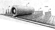
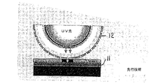
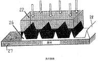
この一般的なフォトリソグラフィ技法は、ローリングマスクフォトリソグラフィにおいて、図2および3に概略的に例示する連続プロセスで使用されている。ここで、液体フォトポリマーを、ノズル10を介して基材11に塗布する。円筒状ローリングマスク12にフォトポリマー上をローリングさせる。円筒状ローリングマスク12は、UV放射の内部同軸源13を収容している。ローリングマスク12の下流には、現像剤のためのノズル15およびリンス液のためのノズル16がある。
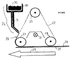
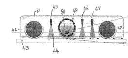
これより図6および7に目を転じて、本開示のある構成について説明する。装置は、装置を覆い、装置を周囲UV光から保護するフードまたはシュラウド41の形をとる。シュラウド内には、装置が基材43にわたって動くことを可能にする一対のローラー42がある。
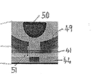
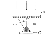
本開示のあるさらなる構成によれば、図8および9に例示するように、マスクレスシステムは、干渉リソグラフィの使用により作製することができる。干渉リソグラフィは、2つのコヒーレントな光源または放射源間の干渉パターンを構築することにより、規則的配列構造の連続パターン形成を可能にする。特徴間の最小間隔は、波長の約半分に等しく、これは、UV放射の場合、約0.2マイクロメートルの最小間隔に対応する。図8に示すように、図6の装置が、円筒状マスク49および光源50の除去、ならびにその代わりとしてのUVレーザー61、空間フィルタ62、ビームスプリッタ63、および一対の鏡64の提供により、変更されている。この構成では、UVレーザーの波長は、364ナノメートルである。鏡64は、角度θを増大または減少させるように、基材43に対して可動性である。これは、干渉構成により生成されるパターン線間の間隔を調節する。
一部の既存のフォトリソグラフィ構成は、表面にわたって望ましい微細構造パターンを層ごとに(例えば、多重露光により)作製するために、多重露光を必要とする。本明細書に記載するのは、多重露光の必要なしに選択された空間プロファイルを有する微細構造パターンを提供する、微細構造パターンを外面上に設けるための方法およびシステムである。
図12は、記載の方法1100において照射するステップ1104を行うように構成された微細構造パターン形成システム1200のある構成を例示する。この構成では、コーティング1152を基材1154に塗布するステップ1102(これはすでに行われている)と未硬化の光硬化性材料を除去するステップ1106(これはまだ行われていない)とは、システム1200によってではなく、別々に行われる。
一構成では、硬化は、ボトムアップ式硬化を含む。図11B〜11Cに例示する例を参照すると、ボトムアップ式硬化は、光硬化性材料の層の外面から近位の第1の側(すなわち、底部側1162)で始まり、外面から遠位の対向する第2の側(すなわち、頂部側1164)に向かって続く硬化プロセスを指す。ボトムアップ式硬化がない場合、硬化は、照射時に瞬間的またはほぼ瞬間的であってもよい。逆に、ボトムアップ式硬化は、硬化が、底部側1162から頂部側1164に空間的かつ経時的に進行することを可能にする。ボトムアップ式硬化は、次のこと、すなわち、未硬化の光硬化性材料が除去される、光硬化性材料の層が完全に硬化する、または硬化がさらに進行することが抑止される、のうちのいずれか1つが発生するまで進行し続ける(下のさらなる説明を参照されたい)。したがって、微細構造パターンの最大高さは、次のもの、すなわち、光硬化性材料の層の厚さ、除去するステップ1106のタイミング、および硬化の抑止の程度、のうちの1つ以上により制御され得る。
記載の方法1100は、後処理ステップをさらに含んでもよい。ステップ1106における微細構造パターンの形成後に、方法1100は、硬化済みの光硬化性材料がない基材1154の少なくとも一部分の除去処理ステップまたは付加処理ステップを含んでもよい。図16Aに例示するように、上段の図は、ステップ1106後の方法1100の結果を表す。結果は、硬化済みの光硬化性材料1600により形成される微細構造パターンを、基材1154の上面上に有する。基材1154の上面はまた、硬化済みの光硬化性材料1600がない区域1602を含む。図16Aに例示する除去処理の場合、方法1110は、例えば基材1154の上面にエッチングまたはサンドブラスト加工を行い、その後硬化済みの光硬化性材料1600を除去することにより、基材1154の一部を除去するステップをさらに含む。除去処理の結果は、ステップ1106の結果の微細構造パターンに対応する微細構造パターンを含む、基材のみの材料である。あるいは、図16Bに例示する付加処理の場合、方法1110は、例えば、追加の基材材料を基材1154の上面上に堆積させ、その後硬化済みの光硬化性材料1600を除去することにより、追加の基材材料を添加することをさらに含む。付加処理の結果は、ステップ1106の結果の微細構造パターン(のネガ)に対応する微細構造パターンを含む、基材のみの材料である。
Claims (18)
- マイクロ構造パターンを基材の外面上に設ける方法であって、
光硬化性材料の層を前記基材の外面に塗布するステップであって、前記塗布済みの光硬化性材料の層が、前記基材の外面から近位の第1の側と、前記基材の外面から遠位の対向する第2の側とを有する、ステップと、
前記光硬化性材料の前記塗布済みの層の前記第2の側上に放射を照射して、前記光硬化性材料の前記層内で、前記第1の側に向かってのより高い硬化速度と、前記第2の側の近くのより低い硬化速度とを含む差別的な硬化速度を生じさせることにより、前記照射済みの光硬化性材料の硬化を前記第1の側から前記第2の側に向かって進行させるステップと、
前記マイクロ構造パターンを形成するために、未硬化の光硬化性材料を除去するステップと、を含む、方法。 - 前記光硬化性材料に照射するステップが、フォトマスクを通じて前記光硬化性材料に照射するステップを含む、請求項1に記載の方法。
- 前記照射するステップが、前記光硬化性材料に所定の持続時間にわたって照射するステップを含み、前記硬化の進行が、非一定の硬化深さプロファイルを形成し、当該ステップ又は未硬化の光硬化性材料を除去するステップが、前記非一定の硬化深さプロファイルのマイクロ構造を有する前記マイクロ構造パターンを形成する、請求項1または2に記載の方法。
- 前記硬化の進行が、前記光硬化性材料の前記層にわたって、前記放射の所定の強度プロファイルに対応し、前記マイクロ構造パターンにおいて、マイクロ構造にわたる高さのばらつきを含む硬化深さプロファイルを生じさせる、請求項1〜3のいずれか一項に記載の方法。
- 前記硬化が、前記光硬化性材料の前記層内への酸素の拡散レベルに基づく前記光硬化性材料の前記層の一部分の硬化の抑止を含む、請求項4に記載の方法。
- 前記第2の側の近くの前記酸素の拡散レベルが、前記光硬化性材料の前記層の前記第1の側の近くのレベルよりも大きい、請求項5に記載の方法。
- 前記硬化の抑止がさらに、露光時間および/または強度に基づく、請求項5または6に記載の方法。
- 前記硬化の抑止が、前記光硬化性材料内の重合を抑止する、請求項5〜7のいずれか一項に記載の方法。
- 前記所定の照射強度プロファイルが、前記照射済みの光硬化性材料の層にわたって対応する周期的な硬化深さプロファイルを生じさせる周期的な強度プロファイルを含む、請求項4〜8のいずれか一項に記載の方法。
- 前記周期的な硬化深さプロファイルが、前記照射済みの光硬化性材料の層にわたっての第1の次元における周期性と、前記照射済みの光硬化性材料の層にわたっての前記第1の次元に直交する第2の次元における実質的に非周期的なプロファイルとを含む、請求項9に記載の方法。
- 前記実質的に非周期的なプロファイルを提供するために、前記基材の外面に対して前記放射を前記第2の次元に沿って移動させるステップをさらに含む、請求項10に記載の方法。
- 前記第1の次元における前記周期性が、以下のマイクロ構造パターン
・のこぎり歯リブレット幾何形状
・波形リブレット幾何形状、および
・刃形リブレット幾何形状
のうちの任意の1つ以上を形成させる、請求項11に記載の方法。 - 前記周期的な硬化深さプロファイルが、前記照射済みの光硬化性材料の層にわたっての第1の次元における周期性と、前記照射済みの光硬化性材料の層にわたっての前記第1の次元に直交する第2の次元における周期性とを含む、請求項9に記載の方法。
- 前記第1の次元における前記周期性と、前記第2の次元における前記周期性とが、以下のマイクロ構造パターン
・蓮の葉の幾何形状、および
・スーパーオムニフォビックな幾何形状
のうちのいずれかまたは両方を生じさせる、請求項13に記載の方法。 - 前記マイクロ構造パターンの形成後に、硬化した光硬化性材料がない前記基材の外面の少なくとも一部分を除去するステップをさらに含む、請求項1〜14のいずれか一項に記載の方法。
- 前記マイクロ構造パターンの形成後に、硬化した光硬化性材料がない前記基材の外面の少なくとも一部分に追加の基材材料を付加するステップをさらに含む、請求項1〜14のいずれか一項に記載の方法。
- 照射するステップが、前記塗布済みの光硬化性材料の層から調節可能な距離に位置付けられたフォトマスクを介して、前記塗布済みの光硬化性材料の層に照射するステップを含む、請求項2〜15のいずれか一項に記載の方法。
- 照射するステップが、前記塗布済みの光硬化性材料の層に405nmで照射するステップを含む、請求項1〜17のいずれか一項に記載の方法。
Priority Applications (1)
| Application Number | Priority Date | Filing Date | Title |
|---|---|---|---|
| JP2021183892A JP2022024037A (ja) | 2015-10-13 | 2021-11-11 | 微細構造パターン |
Applications Claiming Priority (3)
| Application Number | Priority Date | Filing Date | Title |
|---|---|---|---|
| US201562240708P | 2015-10-13 | 2015-10-13 | |
| US62/240,708 | 2015-10-13 | ||
| PCT/AU2016/050960 WO2017063040A1 (en) | 2015-10-13 | 2016-10-13 | Microstructure patterns |
Related Child Applications (1)
| Application Number | Title | Priority Date | Filing Date |
|---|---|---|---|
| JP2021183892A Division JP2022024037A (ja) | 2015-10-13 | 2021-11-11 | 微細構造パターン |
Publications (3)
| Publication Number | Publication Date |
|---|---|
| JP2018531785A JP2018531785A (ja) | 2018-11-01 |
| JP6981663B2 true JP6981663B2 (ja) | 2021-12-15 |
| JP6981663B6 JP6981663B6 (ja) | 2022-01-17 |
Family
ID=58516929
Family Applications (2)
| Application Number | Title | Priority Date | Filing Date |
|---|---|---|---|
| JP2018518969A Active JP6981663B6 (ja) | 2015-10-13 | 2016-10-13 | 微細構造パターン |
| JP2021183892A Pending JP2022024037A (ja) | 2015-10-13 | 2021-11-11 | 微細構造パターン |
Family Applications After (1)
| Application Number | Title | Priority Date | Filing Date |
|---|---|---|---|
| JP2021183892A Pending JP2022024037A (ja) | 2015-10-13 | 2021-11-11 | 微細構造パターン |
Country Status (10)
| Country | Link |
|---|---|
| US (2) | US10877377B2 (ja) |
| EP (2) | EP4063952A1 (ja) |
| JP (2) | JP6981663B6 (ja) |
| CN (1) | CN108369371A (ja) |
| AU (1) | AU2016340034B2 (ja) |
| CA (1) | CA3001742C (ja) |
| PH (1) | PH12018500787A1 (ja) |
| SG (1) | SG11201802842QA (ja) |
| TW (1) | TWI764946B (ja) |
| WO (1) | WO2017063040A1 (ja) |
Families Citing this family (15)
| Publication number | Priority date | Publication date | Assignee | Title |
|---|---|---|---|---|
| JP6981663B6 (ja) | 2015-10-13 | 2022-01-17 | マイクロタウ アイピー ピーティーワイ リミテッド | 微細構造パターン |
| DE102017206968B4 (de) | 2017-04-26 | 2019-10-10 | 4Jet Microtech Gmbh & Co. Kg | Verfahren und Vorrichtung zum Herstellen von Riblets |
| DE102017218543A1 (de) | 2017-10-17 | 2019-04-18 | Lufthansa Technik Ag | Strömungsoptimierte Oberfläche und Fahrzeug mit einer derartigen strömungsoptimierten Oberfläche |
| WO2020131185A2 (en) | 2018-09-26 | 2020-06-25 | Dvorchak Enterprises Llc | One component uv curable compositions and methods for making same |
| CN113631389B (zh) | 2019-03-26 | 2024-03-15 | 日东电工株式会社 | 层叠膜的制造方法 |
| AU2020282386B2 (en) * | 2019-05-30 | 2021-12-16 | Microtau Ip Pty Ltd | Systems and methods for fabricating microstructures |
| CN110655622B (zh) * | 2019-09-04 | 2023-05-05 | 华东理工大学 | 一种基于无掩模光刻系统制备聚合物刷微图案的方法 |
| CN111409265B (zh) | 2020-03-27 | 2021-08-20 | 伊诺福科光学技术有限公司 | 用于加工光纤光栅的纤芯自动聚焦方法及系统、存储介质 |
| US20220072743A1 (en) * | 2020-06-26 | 2022-03-10 | The Research Foundation For The State University Of New York | Thermoplastic components, systems, and methods for forming same |
| CN111880254B (zh) * | 2020-07-14 | 2021-05-14 | 浙江大学 | 一种衍射效率连续变化的光栅的制备方法 |
| CN112708401B (zh) * | 2020-12-24 | 2021-07-27 | 广东工业大学 | 一种具有微型热结构图案的石墨烯薄膜的加工系统及方法 |
| CN113527740A (zh) * | 2021-07-15 | 2021-10-22 | 伊诺福科光学技术有限公司 | 一种具有表面周期性微纳结构的辐射制冷薄膜及制备方法 |
| EP4459269A4 (en) | 2021-12-28 | 2025-10-29 | Nikon Corp | OPTICAL DEVICE AND INSPECTION METHOD |
| EP4491320A4 (en) * | 2022-03-10 | 2026-02-25 | Nikon Corp | TREATMENT DEVICE |
| EP4737847A1 (en) | 2023-06-28 | 2026-05-06 | Nikon Corporation | Optical device and inspection method |
Family Cites Families (53)
| Publication number | Priority date | Publication date | Assignee | Title |
|---|---|---|---|---|
| US4402571A (en) * | 1981-02-17 | 1983-09-06 | Polaroid Corporation | Method for producing a surface relief pattern |
| JPS59143158A (ja) * | 1983-02-07 | 1984-08-16 | W R Gureesu:Kk | 印刷版の製造方法 |
| DE3534293A1 (de) * | 1985-09-26 | 1987-04-02 | Messerschmitt Boelkow Blohm | Einrichtung zur verringerung des reibungswiderstandes |
| GB2226970B (en) * | 1989-01-11 | 1992-10-21 | British Aerospace | Methods of manufacture and surface treatment using laser radiation |
| JPH0580527A (ja) * | 1991-09-20 | 1993-04-02 | Fujitsu Ltd | 干渉露光に関わる半導体装置の製造方法 |
| JP3504426B2 (ja) * | 1995-03-17 | 2004-03-08 | 株式会社荏原製作所 | エネルギービームによる処理方法および処理装置 |
| US6233044B1 (en) * | 1997-01-21 | 2001-05-15 | Steven R. J. Brueck | Methods and apparatus for integrating optical and interferometric lithography to produce complex patterns |
| EP0880078A3 (en) * | 1997-05-23 | 2001-02-14 | Canon Kabushiki Kaisha | Position detection device, apparatus using the same, exposure apparatus, and device manufacturing method using the same |
| JPH11233428A (ja) * | 1998-02-12 | 1999-08-27 | Nikon Corp | 露光装置および素子製造方法 |
| JP3262074B2 (ja) * | 1998-06-30 | 2002-03-04 | キヤノン株式会社 | 露光方法及び露光装置 |
| US6345791B1 (en) | 2000-04-13 | 2002-02-12 | Lockheed Martin Corporation | Streamwise variable height riblets for reducing skin friction drag of surfaces |
| US6858379B2 (en) | 2001-03-22 | 2005-02-22 | Shipley Company, L.L.C. | Photoresist compositions for short wavelength imaging |
| JP4203310B2 (ja) * | 2002-12-09 | 2008-12-24 | 富士フイルム株式会社 | 防眩性反射防止フィルムの製造方法 |
| JP4280509B2 (ja) * | 2003-01-31 | 2009-06-17 | キヤノン株式会社 | 投影露光用マスク、投影露光用マスクの製造方法、投影露光装置および投影露光方法 |
| KR100845565B1 (ko) | 2003-12-01 | 2008-07-10 | 더 보드 오브 트러스티즈 오브 더 유니버시티 오브 일리노이 | 나노스케일 3차원 구조물의 제조방법 및 장치 |
| US20050260013A1 (en) * | 2004-05-20 | 2005-11-24 | Bert Vanlathem | Digital control strip for flexogaphic printing |
| US20050271973A1 (en) | 2004-06-04 | 2005-12-08 | Ziegler Michael J | Negative acting photoresist with improved blocking resistance |
| JP4389791B2 (ja) | 2004-08-25 | 2009-12-24 | セイコーエプソン株式会社 | 微細構造体の製造方法および露光装置 |
| EP1810085B1 (en) | 2004-10-22 | 2011-03-16 | Eulitha AG | A system and a method for generating periodic and/or quasi-periodic pattern on a sample |
| JP2006339359A (ja) * | 2005-06-01 | 2006-12-14 | Seiko Epson Corp | 微細構造体の製造方法、電子機器 |
| DE102005031057A1 (de) * | 2005-07-02 | 2007-01-04 | Punch Graphix Prepress Germany Gmbh | Verfahren zur Belichtung von Flexodruckplatten |
| JP2007264224A (ja) * | 2006-03-28 | 2007-10-11 | Dainippon Printing Co Ltd | 印刷版製造用マスク、印刷版及び印刷版の製造方法 |
| JP2008064903A (ja) * | 2006-09-06 | 2008-03-21 | National Institute Of Advanced Industrial & Technology | 三次元構造物作製装置、センサー作製装置、及び三次元構造物作製方法 |
| US7709187B2 (en) * | 2006-10-23 | 2010-05-04 | International Business Machines Corporation | High resolution imaging process using an in-situ image modifying layer |
| DE102007021249A1 (de) * | 2007-05-07 | 2008-11-20 | Singulus Technologies Ag | Sauerstoff-Inhibierung eines härtbaren Materials beim Strukturieren von Substraten |
| US8236480B2 (en) | 2007-05-24 | 2012-08-07 | The United States of America, as represented by the Secretary of Commere, the National Institute of Standards and Technology | Fabrication method of topographically modulated microstructures using pattern homogenization with UV light |
| FR2921862B1 (fr) | 2007-10-05 | 2011-04-22 | Macdermid Printing Solutions Europ Sas | Procede de realisation d'un agencement a image en relief utilisable notamment dans le domaine de la flexographie et agencement realise selon ce procede |
| US8399179B2 (en) | 2008-04-24 | 2013-03-19 | Hewlett-Packard Development Company, L.P. | High aspect ratio microstructures |
| US20100003605A1 (en) * | 2008-07-07 | 2010-01-07 | International Business Machines Corporation | system and method for projection lithography with immersed image-aligned diffractive element |
| JP5521354B2 (ja) | 2009-02-27 | 2014-06-11 | 三菱レイヨン株式会社 | 微細凹凸構造を表面に有する透明フィルムおよびその製造方法 |
| US8124193B2 (en) | 2009-03-09 | 2012-02-28 | Xerox Corporation | Gloss control of UV curable formulations through micro-patterning |
| US8367306B1 (en) | 2009-07-13 | 2013-02-05 | Hrl Laboratories, Llc | Method of continuous or batch fabrication of large area polymer micro-truss structured materials |
| JP2011118344A (ja) * | 2009-11-02 | 2011-06-16 | Mejiro Precision:Kk | 3次元パターン形成方法 |
| EP2499539B1 (en) | 2009-11-13 | 2014-06-18 | Eulitha AG | Optimized mask design for fabricating periodic and quasi-periodic patterns |
| US8368871B2 (en) | 2010-02-16 | 2013-02-05 | Eulitha Ag | Lithographic fabrication of general periodic structures |
| US9036133B2 (en) | 2010-02-16 | 2015-05-19 | Eulitha Ag | Lithographic fabrication of general periodic structures by exposing a photosensitive layer to a range of lateral intensity distributions |
| US9007566B2 (en) | 2010-07-07 | 2015-04-14 | Eulitha Ag | Apparatus and method for printing a periodic pattern with a large depth of focus |
| US8524443B2 (en) | 2010-07-07 | 2013-09-03 | Eulitha A.G. | Method and apparatus for printing a periodic pattern with a large depth of focus |
| CN103154319B (zh) * | 2010-10-06 | 2016-08-10 | 3M创新有限公司 | 具有基于纳米二氧化硅的涂层和阻挡层的抗反射制品 |
| US8525973B2 (en) | 2010-10-13 | 2013-09-03 | Eulitha A.G. | Method and apparatus for printing periodic patterns |
| WO2012066489A2 (en) | 2010-11-16 | 2012-05-24 | Eulitha A.G. | Method and apparatus for printing high-resolution two-dimensional periodic patterns |
| JP5721858B2 (ja) | 2010-12-23 | 2015-05-20 | ユーリタ アクチエンゲゼルシャフトEulitha Ag | 大きな面積にわたってナノ構造を製造するためのシステムおよび方法 |
| EP2663898B1 (en) | 2011-01-12 | 2015-03-25 | Eulitha A.G. | Method and system for printing high-resolution periodic patterns |
| US8772740B2 (en) * | 2011-04-08 | 2014-07-08 | Esko-Graphics Imaging Gmbh | UV curing creating flattop and roundtop structures on a single printing plate |
| EP2715453A1 (en) | 2011-06-01 | 2014-04-09 | Eulitha A.G. | Printing periodic patterns using multiple lasers |
| JP2013026283A (ja) * | 2011-07-15 | 2013-02-04 | Toshiba Corp | 干渉露光装置 |
| CN102955365B (zh) * | 2011-08-22 | 2014-12-17 | 上海微电子装备有限公司 | 一种干涉曝光装置及方法 |
| US20130337386A1 (en) * | 2012-06-14 | 2013-12-19 | Dirk De Rauw | Processing apparatus for processing a flexographic plate, a method and a computer program product |
| US20140272237A1 (en) * | 2013-03-15 | 2014-09-18 | Prc-Desoto International, Inc. | Strippable film assembly and coating for drag reduction |
| US9658535B2 (en) | 2013-03-18 | 2017-05-23 | Eulitha A.G. | Methods and systems for printing periodic patterns |
| US20150248060A1 (en) | 2014-02-28 | 2015-09-03 | Konica Minolta Laboratory U.S.A., Inc. | Method of making thermal insulation film and thermal insulation film product |
| WO2016115640A1 (en) * | 2015-01-23 | 2016-07-28 | Li Minggan | Methods and apparatus for creation of wrinkles in three-dimensional surfaces, and compositions of matter resulting from same |
| JP6981663B6 (ja) | 2015-10-13 | 2022-01-17 | マイクロタウ アイピー ピーティーワイ リミテッド | 微細構造パターン |
-
2016
- 2016-10-13 JP JP2018518969A patent/JP6981663B6/ja active Active
- 2016-10-13 AU AU2016340034A patent/AU2016340034B2/en active Active
- 2016-10-13 CN CN201680072839.3A patent/CN108369371A/zh active Pending
- 2016-10-13 WO PCT/AU2016/050960 patent/WO2017063040A1/en not_active Ceased
- 2016-10-13 EP EP22173388.4A patent/EP4063952A1/en not_active Withdrawn
- 2016-10-13 EP EP16854644.8A patent/EP3362855B1/en active Active
- 2016-10-13 CA CA3001742A patent/CA3001742C/en active Active
- 2016-10-13 US US15/767,990 patent/US10877377B2/en active Active
- 2016-10-13 SG SG11201802842QA patent/SG11201802842QA/en unknown
-
2017
- 2017-10-12 TW TW106134935A patent/TWI764946B/zh active
-
2018
- 2018-04-12 PH PH12018500787A patent/PH12018500787A1/en unknown
-
2020
- 2020-12-17 US US17/126,020 patent/US20210165330A1/en not_active Abandoned
-
2021
- 2021-11-11 JP JP2021183892A patent/JP2022024037A/ja active Pending
Also Published As
| Publication number | Publication date |
|---|---|
| CN108369371A (zh) | 2018-08-03 |
| JP6981663B6 (ja) | 2022-01-17 |
| US10877377B2 (en) | 2020-12-29 |
| JP2022024037A (ja) | 2022-02-08 |
| TW201825201A (zh) | 2018-07-16 |
| SG11201802842QA (en) | 2018-05-30 |
| EP3362855A4 (en) | 2019-07-03 |
| AU2016340034B2 (en) | 2021-05-06 |
| AU2016340034A1 (en) | 2018-05-10 |
| CA3001742C (en) | 2023-02-28 |
| JP2018531785A (ja) | 2018-11-01 |
| TWI764946B (zh) | 2022-05-21 |
| US20210165330A1 (en) | 2021-06-03 |
| EP3362855B1 (en) | 2022-11-30 |
| EP4063952A1 (en) | 2022-09-28 |
| PH12018500787A1 (en) | 2018-10-29 |
| US20180307138A1 (en) | 2018-10-25 |
| CA3001742A1 (en) | 2017-04-20 |
| EP3362855A1 (en) | 2018-08-22 |
| WO2017063040A1 (en) | 2017-04-20 |
| NZ740947A (en) | 2021-09-24 |
Similar Documents
| Publication | Publication Date | Title |
|---|---|---|
| JP6981663B2 (ja) | 微細構造パターン | |
| US6730256B1 (en) | Stereolithographic patterning with interlayer surface modifications | |
| Skliutas et al. | Polymerization mechanisms initiated by spatio-temporally confined light | |
| KR100845565B1 (ko) | 나노스케일 3차원 구조물의 제조방법 및 장치 | |
| US8017193B1 (en) | Monomeric formulation for making polymer waveguides | |
| CN110573291B (zh) | 通过激光光刻制造3d结构的方法及相应的计算机程序产品 | |
| Mironov et al. | Photolithography in the vacuum ultraviolet (172 nm) with sub-400 nm resolution: photoablative patterning of nanostructures and optical components in bulk polymers and thin films on semiconductors | |
| US10509327B1 (en) | Variable neutral density filter for multi-beam interference lithography exposure | |
| US20190287792A1 (en) | Method of manufacturing integrated circuit device | |
| Bilinsky | Riblet Microfabrication method for drag reduction | |
| Haq et al. | Vertical sidewalls in thick epoxy resists–a challenge for laser-based direct write lithography | |
| JP7587863B2 (ja) | 微細構造体を製造するためのシステム及び方法 | |
| Choi et al. | Marangoni‐Driven Patterning in Polymer Thin Film Supported on Shrinking Substrate for Resolution Enhancement | |
| NZ740947B2 (en) | Microstructure patterns | |
| KR100746332B1 (ko) | 광가교 가능한 콜로이드 입자를 이용한 다차원 나노패턴형성방법 | |
| CN104303108A (zh) | 利用负对比组合物的多光子固化方法 | |
| Perez-Murano et al. | Optical lithography | |
| KR101105378B1 (ko) | 광간섭 리소그래피에 의한 멀티스케일 격자 패턴 형성 방법 | |
| US20240351272A1 (en) | Projection two-photon lithography method and system for rapid printing of 3d structures with sub-micrometer features and porosities | |
| Yuan | Laser direct-write microfabrication and patterning | |
| Seo et al. | Spatial light modulation based 3D lithography with single scan virtual layering | |
| MIZUTANI et al. | Fabrication of layered nanostructure in large area by 3D lithography using Talbot effect | |
| Rumler et al. | One-step fabrication of hierarchical structures by direct laser writing through PDMS molds | |
| KR20190060591A (ko) | 펄스 자외선을 이용한 폴리실라잔계 소재 박막의 패터닝 및 이의 제조방법 | |
| KR20120039389A (ko) | 반도체 소자의 패턴 형성 방법 |
Legal Events
| Date | Code | Title | Description |
|---|---|---|---|
| A529 | Written submission of copy of amendment under article 34 pct |
Free format text: JAPANESE INTERMEDIATE CODE: A529 Effective date: 20180605 |
|
| A621 | Written request for application examination |
Free format text: JAPANESE INTERMEDIATE CODE: A621 Effective date: 20190808 |
|
| A977 | Report on retrieval |
Free format text: JAPANESE INTERMEDIATE CODE: A971007 Effective date: 20200715 |
|
| A131 | Notification of reasons for refusal |
Free format text: JAPANESE INTERMEDIATE CODE: A131 Effective date: 20200804 |
|
| A601 | Written request for extension of time |
Free format text: JAPANESE INTERMEDIATE CODE: A601 Effective date: 20201028 |
|
| A521 | Request for written amendment filed |
Free format text: JAPANESE INTERMEDIATE CODE: A523 Effective date: 20201223 |
|
| A131 | Notification of reasons for refusal |
Free format text: JAPANESE INTERMEDIATE CODE: A131 Effective date: 20210427 |
|
| A521 | Request for written amendment filed |
Free format text: JAPANESE INTERMEDIATE CODE: A523 Effective date: 20210726 |
|
| TRDD | Decision of grant or rejection written | ||
| A01 | Written decision to grant a patent or to grant a registration (utility model) |
Free format text: JAPANESE INTERMEDIATE CODE: A01 Effective date: 20211012 |
|
| A61 | First payment of annual fees (during grant procedure) |
Free format text: JAPANESE INTERMEDIATE CODE: A61 Effective date: 20211111 |
|
| R150 | Certificate of patent or registration of utility model |
Ref document number: 6981663 Country of ref document: JP Free format text: JAPANESE INTERMEDIATE CODE: R150 |
|
| R250 | Receipt of annual fees |
Free format text: JAPANESE INTERMEDIATE CODE: R250 |
|
| R250 | Receipt of annual fees |
Free format text: JAPANESE INTERMEDIATE CODE: R250 |