JP6976768B2 - 電源装置及び画像形成装置 - Google Patents
電源装置及び画像形成装置 Download PDFInfo
- Publication number
- JP6976768B2 JP6976768B2 JP2017154665A JP2017154665A JP6976768B2 JP 6976768 B2 JP6976768 B2 JP 6976768B2 JP 2017154665 A JP2017154665 A JP 2017154665A JP 2017154665 A JP2017154665 A JP 2017154665A JP 6976768 B2 JP6976768 B2 JP 6976768B2
- Authority
- JP
- Japan
- Prior art keywords
- rectifying
- transformer
- voltage
- power supply
- secondary winding
- Prior art date
- Legal status (The legal status is an assumption and is not a legal conclusion. Google has not performed a legal analysis and makes no representation as to the accuracy of the status listed.)
- Active
Links
Images


Classifications
-
- G—PHYSICS
- G03—PHOTOGRAPHY; CINEMATOGRAPHY; ANALOGOUS TECHNIQUES USING WAVES OTHER THAN OPTICAL WAVES; ELECTROGRAPHY; HOLOGRAPHY
- G03G—ELECTROGRAPHY; ELECTROPHOTOGRAPHY; MAGNETOGRAPHY
- G03G15/00—Apparatus for electrographic processes using a charge pattern
- G03G15/50—Machine control of apparatus for electrographic processes using a charge pattern, e.g. regulating differents parts of the machine, multimode copiers, microprocessor control
- G03G15/5004—Power supply control, e.g. power-saving mode, automatic power turn-off
-
- G—PHYSICS
- G03—PHOTOGRAPHY; CINEMATOGRAPHY; ANALOGOUS TECHNIQUES USING WAVES OTHER THAN OPTICAL WAVES; ELECTROGRAPHY; HOLOGRAPHY
- G03G—ELECTROGRAPHY; ELECTROPHOTOGRAPHY; MAGNETOGRAPHY
- G03G15/00—Apparatus for electrographic processes using a charge pattern
- G03G15/02—Apparatus for electrographic processes using a charge pattern for laying down a uniform charge, e.g. for sensitising; Corona discharge devices
- G03G15/0283—Arrangements for supplying power to the sensitising device
-
- G—PHYSICS
- G03—PHOTOGRAPHY; CINEMATOGRAPHY; ANALOGOUS TECHNIQUES USING WAVES OTHER THAN OPTICAL WAVES; ELECTROGRAPHY; HOLOGRAPHY
- G03G—ELECTROGRAPHY; ELECTROPHOTOGRAPHY; MAGNETOGRAPHY
- G03G15/00—Apparatus for electrographic processes using a charge pattern
- G03G15/14—Apparatus for electrographic processes using a charge pattern for transferring a pattern to a second base
- G03G15/16—Apparatus for electrographic processes using a charge pattern for transferring a pattern to a second base of a toner pattern, e.g. a powder pattern, e.g. magnetic transfer
- G03G15/1665—Apparatus for electrographic processes using a charge pattern for transferring a pattern to a second base of a toner pattern, e.g. a powder pattern, e.g. magnetic transfer by introducing the second base in the nip formed by the recording member and at least one transfer member, e.g. in combination with bias or heat
- G03G15/167—Apparatus for electrographic processes using a charge pattern for transferring a pattern to a second base of a toner pattern, e.g. a powder pattern, e.g. magnetic transfer by introducing the second base in the nip formed by the recording member and at least one transfer member, e.g. in combination with bias or heat at least one of the recording member or the transfer member being rotatable during the transfer
- G03G15/1675—Apparatus for electrographic processes using a charge pattern for transferring a pattern to a second base of a toner pattern, e.g. a powder pattern, e.g. magnetic transfer by introducing the second base in the nip formed by the recording member and at least one transfer member, e.g. in combination with bias or heat at least one of the recording member or the transfer member being rotatable during the transfer with means for controlling the bias applied in the transfer nip
-
- G—PHYSICS
- G03—PHOTOGRAPHY; CINEMATOGRAPHY; ANALOGOUS TECHNIQUES USING WAVES OTHER THAN OPTICAL WAVES; ELECTROGRAPHY; HOLOGRAPHY
- G03G—ELECTROGRAPHY; ELECTROPHOTOGRAPHY; MAGNETOGRAPHY
- G03G15/00—Apparatus for electrographic processes using a charge pattern
- G03G15/14—Apparatus for electrographic processes using a charge pattern for transferring a pattern to a second base
- G03G15/16—Apparatus for electrographic processes using a charge pattern for transferring a pattern to a second base of a toner pattern, e.g. a powder pattern, e.g. magnetic transfer
- G03G15/1665—Apparatus for electrographic processes using a charge pattern for transferring a pattern to a second base of a toner pattern, e.g. a powder pattern, e.g. magnetic transfer by introducing the second base in the nip formed by the recording member and at least one transfer member, e.g. in combination with bias or heat
- G03G15/167—Apparatus for electrographic processes using a charge pattern for transferring a pattern to a second base of a toner pattern, e.g. a powder pattern, e.g. magnetic transfer by introducing the second base in the nip formed by the recording member and at least one transfer member, e.g. in combination with bias or heat at least one of the recording member or the transfer member being rotatable during the transfer
- G03G15/168—Apparatus for electrographic processes using a charge pattern for transferring a pattern to a second base of a toner pattern, e.g. a powder pattern, e.g. magnetic transfer by introducing the second base in the nip formed by the recording member and at least one transfer member, e.g. in combination with bias or heat at least one of the recording member or the transfer member being rotatable during the transfer with means for conditioning the transfer element, e.g. cleaning
-
- G—PHYSICS
- G03—PHOTOGRAPHY; CINEMATOGRAPHY; ANALOGOUS TECHNIQUES USING WAVES OTHER THAN OPTICAL WAVES; ELECTROGRAPHY; HOLOGRAPHY
- G03G—ELECTROGRAPHY; ELECTROPHOTOGRAPHY; MAGNETOGRAPHY
- G03G15/00—Apparatus for electrographic processes using a charge pattern
- G03G15/80—Details relating to power supplies, circuits boards, electrical connections
-
- H—ELECTRICITY
- H02—GENERATION; CONVERSION OR DISTRIBUTION OF ELECTRIC POWER
- H02M—APPARATUS FOR CONVERSION BETWEEN AC AND AC, BETWEEN AC AND DC, OR BETWEEN DC AND DC, AND FOR USE WITH MAINS OR SIMILAR POWER SUPPLY SYSTEMS; CONVERSION OF DC OR AC INPUT POWER INTO SURGE OUTPUT POWER; CONTROL OR REGULATION THEREOF
- H02M3/00—Conversion of dc power input into dc power output
- H02M3/22—Conversion of dc power input into dc power output with intermediate conversion into ac
- H02M3/24—Conversion of dc power input into dc power output with intermediate conversion into ac by static converters
- H02M3/28—Conversion of dc power input into dc power output with intermediate conversion into ac by static converters using discharge tubes with control electrode or semiconductor devices with control electrode to produce the intermediate ac
- H02M3/325—Conversion of dc power input into dc power output with intermediate conversion into ac by static converters using discharge tubes with control electrode or semiconductor devices with control electrode to produce the intermediate ac using devices of a triode or a transistor type requiring continuous application of a control signal
- H02M3/335—Conversion of dc power input into dc power output with intermediate conversion into ac by static converters using discharge tubes with control electrode or semiconductor devices with control electrode to produce the intermediate ac using devices of a triode or a transistor type requiring continuous application of a control signal using semiconductor devices only
Description
また、以上の課題を解決するために、電源装置は、トランスと、前記トランスの二次巻線に発生する交流電圧を整流平滑する第一の整流平滑手段と、前記トランスの二次巻線に発生する交流電圧を入力とし、交流成分を分離した交流電圧を出力する分離手段と、前記分離手段の出力を整流平滑する第二の整流平滑手段と、前記分離手段と前記第二の整流平滑手段とを接続するラインから分岐したラインに配置される抵抗器と、前記抵抗器に直列して接続され且つ基準に接続された整流手段と、制御手段と、備え、前記整流手段は、トランジスタを含み、前記制御手段は、前記二次巻線に発生する負電圧のピークに応じた時間、電流を流すように、前記トランジスタのスイッチング制御を行うことを特徴とする。
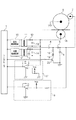
図6に示した電源装置では、コンデンサ4に負の電圧が充電されてしまう。以下、その充電メカニズムと、その充電により引き起こされる問題点について図7を用い説明する。
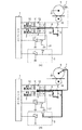
図2(a)、図2(b)はトランス3の二次巻線に発生する高電圧によって、ダイオード15のカソード側の電位が正となった場合と負となった場合における、コンデンサ4を流れる電流の経路を示している。これらは図7(a)、図7(b)の場合とは異なる。
上で説明したように、コンデンサ4の充電電圧が小さくなればそれに応じた効果を得ることができるが、よりゼロに近いほうが望ましい。以下、コンデンサ4への充電をより効果的に抑制する為の抵抗値の決定方法について説明する。ここでは一例として、トランス3の二次巻線に図3で示される高電圧が発生するケースを説明する。

4 交流分離コンデンサ
7 帯電ローラ
8 感光ドラム
9 電圧検知回路
16 転写ローラ
17 電流検知回路
18 抵抗器
19 整流ダイオード
20 整流トランジスタ
Claims (6)
- 電源装置であって、
トランスと、
前記トランスの二次巻線に発生する交流電圧を整流平滑する第一の整流平滑手段と、
前記トランスの二次巻線に発生する交流電圧を入力とし、交流成分を分離した交流電圧を出力する分離手段と、
前記分離手段の出力を整流平滑する第二の整流平滑手段と、
前記分離手段と前記第二の整流平滑手段とを接続するラインから分岐したラインに配置される抵抗器と、
前記抵抗器に直列して接続され且つ基準に接続された整流手段と、を備え、
前記整流手段は、前記分離手段から前記基準への電流を流し、前記基準から前記分離手段への電流を遮断し、
前記抵抗器は、前記二次巻線に発生する電圧が正のときに前記分離手段により流れる第一電流と前記二次巻線に発生する電圧が負のときに前記分離手段により流れる第二電流との大小関係が、前記第一電流が流れる時間と前記第二電流が流れる時間の大小関係とは逆になるようにする抵抗値であることを特徴する電源装置。 - 電源装置であって、
トランスと、
前記トランスの二次巻線に発生する交流電圧を整流平滑する第一の整流平滑手段と、
前記トランスの二次巻線に発生する交流電圧を入力とし、交流成分を分離した交流電圧を出力する分離手段と、
前記分離手段の出力を整流平滑する第二の整流平滑手段と、
前記分離手段と前記第二の整流平滑手段とを接続するラインから分岐したラインに配置される抵抗器と、
前記抵抗器に直列して接続され且つ基準に接続された整流手段と、
制御手段と、備え、
前記整流手段は、トランジスタを含み、
前記制御手段は、前記二次巻線に発生する負電圧のピークに応じた時間、電流を流すように、前記トランジスタのスイッチング制御を行うことを特徴とする電源装置。 - 前記制御手段は、前記二次巻線の負電圧のピークが減少した場合に、前記電流を流す時間を減らすように前記トランジスタのスイッチング制御を行うことを特徴とする請求項2に記載の電源装置。
- 前記整流手段は、ダイオード又はトランジスタであることを特徴とする請求項1乃至3の何れか1項に記載の電源装置。
- 前記分離手段は、コンデンサであることを特徴とする請求項1乃至4の何れか1項に記載の電源装置。
- 画像形成装置であって、
表面にトナー像が形成される像担持体と、
前記像担持体を帯電させる帯電部材と、
前記帯電部材により帯電された前記像担持体に静電潜像を形成させる露光器と、
前記静電潜像が形成された前記像担持体にトナーを付着させトナー像を形成する現像器と、
前記像担持体表面に形成されたトナー像を被転写媒体に転写する転写部材と、
請求項1乃至5の何れか1項に記載の電源装置と、を備え、
前記第一の整流平滑手段の出力が前記転写部材に接続され、
前記第二の整流平滑手段の出力が前記帯電部材に接続されることを特徴とする画像形成装置。
Priority Applications (2)
| Application Number | Priority Date | Filing Date | Title |
|---|---|---|---|
| JP2017154665A JP6976768B2 (ja) | 2017-08-09 | 2017-08-09 | 電源装置及び画像形成装置 |
| US16/052,434 US10503108B2 (en) | 2017-08-09 | 2018-08-01 | Power supply apparatus for outputting first and second voltages from one transformer and image forming apparatus including power supply apparatus |
Applications Claiming Priority (1)
| Application Number | Priority Date | Filing Date | Title |
|---|---|---|---|
| JP2017154665A JP6976768B2 (ja) | 2017-08-09 | 2017-08-09 | 電源装置及び画像形成装置 |
Publications (3)
| Publication Number | Publication Date |
|---|---|
| JP2019033645A JP2019033645A (ja) | 2019-02-28 |
| JP2019033645A5 JP2019033645A5 (ja) | 2020-09-10 |
| JP6976768B2 true JP6976768B2 (ja) | 2021-12-08 |
Family
ID=65275012
Family Applications (1)
| Application Number | Title | Priority Date | Filing Date |
|---|---|---|---|
| JP2017154665A Active JP6976768B2 (ja) | 2017-08-09 | 2017-08-09 | 電源装置及び画像形成装置 |
Country Status (2)
| Country | Link |
|---|---|
| US (1) | US10503108B2 (ja) |
| JP (1) | JP6976768B2 (ja) |
Families Citing this family (2)
| Publication number | Priority date | Publication date | Assignee | Title |
|---|---|---|---|---|
| US10488790B2 (en) * | 2017-11-29 | 2019-11-26 | Canon Kabushiki Kaisha | Image forming apparatus having transfer voltage control |
| US11500311B2 (en) * | 2020-12-17 | 2022-11-15 | Canon Kabushiki Kaisha | Image forming apparatus including techniques and mechanisms to suppress occurrence of an image defect caused by a transfer step |
Family Cites Families (9)
| Publication number | Priority date | Publication date | Assignee | Title |
|---|---|---|---|---|
| JPS59172945A (ja) * | 1983-03-22 | 1984-09-29 | Victor Co Of Japan Ltd | 直流高電圧発生装置 |
| ATE196052T1 (de) * | 1994-04-29 | 2000-09-15 | Andre Bonnet | Statischer wandler mit gesteuertem schalter und steuerungsschaltung |
| US5689409A (en) * | 1994-07-27 | 1997-11-18 | Deutsche Thomson-Brandt Gmbh | Switched-mode power supply |
| US5500721A (en) * | 1995-01-03 | 1996-03-19 | Xerox Corporation | Power supply topology enabling bipolar voltage output from a single voltage input |
| DE10137176A1 (de) * | 2001-07-31 | 2003-02-13 | Thomson Brandt Gmbh | Schaltnetzteil mit Dämpfungsnetzwerk |
| JP4908863B2 (ja) | 2006-02-02 | 2012-04-04 | キヤノン株式会社 | 画像形成装置及び高圧電源装置 |
| US8547711B2 (en) * | 2010-11-19 | 2013-10-01 | General Electric Company | LLC converter active snubber circuit and method of operation thereof |
| EP2713488B1 (en) * | 2012-09-28 | 2020-04-15 | OSRAM GmbH | Electronic converter, and related lighting system and method of operating an electronic converter |
| JP6727806B2 (ja) * | 2015-02-18 | 2020-07-22 | キヤノン株式会社 | 電源装置及び画像形成装置 |
-
2017
- 2017-08-09 JP JP2017154665A patent/JP6976768B2/ja active Active
-
2018
- 2018-08-01 US US16/052,434 patent/US10503108B2/en active Active
Also Published As
| Publication number | Publication date |
|---|---|
| US20190049883A1 (en) | 2019-02-14 |
| US10503108B2 (en) | 2019-12-10 |
| JP2019033645A (ja) | 2019-02-28 |
Similar Documents
| Publication | Publication Date | Title |
|---|---|---|
| US9904232B2 (en) | Power supply apparatus and image forming apparatus | |
| JP5382462B2 (ja) | 画像形成装置 | |
| JP6976768B2 (ja) | 電源装置及び画像形成装置 | |
| JP2009229577A (ja) | 画像形成装置 | |
| US9141019B2 (en) | Power-supply device and image formation apparatus | |
| JP5880023B2 (ja) | 電源供給回路、画像形成装置 | |
| JP2018113766A (ja) | 高圧電源装置、画像形成装置 | |
| JP2012048032A (ja) | 画像形成装置および帯電器の制御方法 | |
| JP6727806B2 (ja) | 電源装置及び画像形成装置 | |
| JP5590956B2 (ja) | 画像形成装置及び電源装置 | |
| JPH1032979A (ja) | 定電圧回路、及び定電圧・定電流切換回路 | |
| JP6448305B2 (ja) | 電源装置および画像形成装置 | |
| JP4737247B2 (ja) | 画像形成装置 | |
| JP6613695B2 (ja) | 画像形成装置およびその制御方法 | |
| JP6808438B2 (ja) | 電源装置及び画像形成装置 | |
| JP5321568B2 (ja) | 画像形成装置 | |
| JP6665518B2 (ja) | 画像形成装置および画像形成装置の制御方法 | |
| JP6108193B2 (ja) | 画像形成装置 | |
| US9025979B2 (en) | Image forming apparatus and bias power supply apparatus and method | |
| US8374520B2 (en) | Image forming apparatus | |
| JP6700695B2 (ja) | 電源装置及び画像形成装置 | |
| JP2022079160A (ja) | 画像形成装置 | |
| JP2006201351A (ja) | 画像形成装置 | |
| JP6808437B2 (ja) | 電源装置及び画像形成装置 | |
| US8565629B2 (en) | Image forming apparatus |
Legal Events
| Date | Code | Title | Description |
|---|---|---|---|
| A521 | Written amendment |
Free format text: JAPANESE INTERMEDIATE CODE: A523 Effective date: 20200717 |
|
| A621 | Written request for application examination |
Free format text: JAPANESE INTERMEDIATE CODE: A621 Effective date: 20200717 |
|
| A977 | Report on retrieval |
Free format text: JAPANESE INTERMEDIATE CODE: A971007 Effective date: 20210430 |
|
| A131 | Notification of reasons for refusal |
Free format text: JAPANESE INTERMEDIATE CODE: A131 Effective date: 20210511 |
|
| A521 | Written amendment |
Free format text: JAPANESE INTERMEDIATE CODE: A523 Effective date: 20210705 |
|
| A131 | Notification of reasons for refusal |
Free format text: JAPANESE INTERMEDIATE CODE: A131 Effective date: 20210810 |
|
| A521 | Written amendment |
Free format text: JAPANESE INTERMEDIATE CODE: A523 Effective date: 20210928 |
|
| TRDD | Decision of grant or rejection written | ||
| A01 | Written decision to grant a patent or to grant a registration (utility model) |
Free format text: JAPANESE INTERMEDIATE CODE: A01 Effective date: 20211012 |
|
| A61 | First payment of annual fees (during grant procedure) |
Free format text: JAPANESE INTERMEDIATE CODE: A61 Effective date: 20211110 |
|
| R151 | Written notification of patent or utility model registration |
Ref document number: 6976768 Country of ref document: JP Free format text: JAPANESE INTERMEDIATE CODE: R151 |