JP6962308B2 - ゲート駆動回路 - Google Patents
ゲート駆動回路 Download PDFInfo
- Publication number
- JP6962308B2 JP6962308B2 JP2018230804A JP2018230804A JP6962308B2 JP 6962308 B2 JP6962308 B2 JP 6962308B2 JP 2018230804 A JP2018230804 A JP 2018230804A JP 2018230804 A JP2018230804 A JP 2018230804A JP 6962308 B2 JP6962308 B2 JP 6962308B2
- Authority
- JP
- Japan
- Prior art keywords
- gate
- voltage
- drive circuit
- constant
- gate drive
- Prior art date
- Legal status (The legal status is an assumption and is not a legal conclusion. Google has not performed a legal analysis and makes no representation as to the accuracy of the status listed.)
- Active
Links
Images


Classifications
-
- H—ELECTRICITY
- H03—ELECTRONIC CIRCUITRY
- H03K—PULSE TECHNIQUE
- H03K17/00—Electronic switching or gating, i.e. not by contact-making and –breaking
- H03K17/06—Modifications for ensuring a fully conducting state
-
- H—ELECTRICITY
- H03—ELECTRONIC CIRCUITRY
- H03K—PULSE TECHNIQUE
- H03K17/00—Electronic switching or gating, i.e. not by contact-making and –breaking
- H03K17/08—Modifications for protecting switching circuit against overcurrent or overvoltage
- H03K17/081—Modifications for protecting switching circuit against overcurrent or overvoltage without feedback from the output circuit to the control circuit
- H03K17/0812—Modifications for protecting switching circuit against overcurrent or overvoltage without feedback from the output circuit to the control circuit by measures taken in the control circuit
- H03K17/08126—Modifications for protecting switching circuit against overcurrent or overvoltage without feedback from the output circuit to the control circuit by measures taken in the control circuit in bipolar transitor switches
-
- H—ELECTRICITY
- H02—GENERATION; CONVERSION OR DISTRIBUTION OF ELECTRIC POWER
- H02M—APPARATUS FOR CONVERSION BETWEEN AC AND AC, BETWEEN AC AND DC, OR BETWEEN DC AND DC, AND FOR USE WITH MAINS OR SIMILAR POWER SUPPLY SYSTEMS; CONVERSION OF DC OR AC INPUT POWER INTO SURGE OUTPUT POWER; CONTROL OR REGULATION THEREOF
- H02M1/00—Details of apparatus for conversion
- H02M1/08—Circuits specially adapted for the generation of control voltages for semiconductor devices incorporated in static converters
- H02M1/084—Circuits specially adapted for the generation of control voltages for semiconductor devices incorporated in static converters using a control circuit common to several phases of a multi-phase system
-
- H—ELECTRICITY
- H03—ELECTRONIC CIRCUITRY
- H03K—PULSE TECHNIQUE
- H03K17/00—Electronic switching or gating, i.e. not by contact-making and –breaking
- H03K17/08—Modifications for protecting switching circuit against overcurrent or overvoltage
- H03K17/081—Modifications for protecting switching circuit against overcurrent or overvoltage without feedback from the output circuit to the control circuit
- H03K17/0812—Modifications for protecting switching circuit against overcurrent or overvoltage without feedback from the output circuit to the control circuit by measures taken in the control circuit
- H03K17/08122—Modifications for protecting switching circuit against overcurrent or overvoltage without feedback from the output circuit to the control circuit by measures taken in the control circuit in field-effect transistor switches
-
- H—ELECTRICITY
- H03—ELECTRONIC CIRCUITRY
- H03K—PULSE TECHNIQUE
- H03K17/00—Electronic switching or gating, i.e. not by contact-making and –breaking
- H03K17/08—Modifications for protecting switching circuit against overcurrent or overvoltage
- H03K17/081—Modifications for protecting switching circuit against overcurrent or overvoltage without feedback from the output circuit to the control circuit
- H03K17/0812—Modifications for protecting switching circuit against overcurrent or overvoltage without feedback from the output circuit to the control circuit by measures taken in the control circuit
- H03K17/08128—Modifications for protecting switching circuit against overcurrent or overvoltage without feedback from the output circuit to the control circuit by measures taken in the control circuit in composite switches
-
- H—ELECTRICITY
- H02—GENERATION; CONVERSION OR DISTRIBUTION OF ELECTRIC POWER
- H02M—APPARATUS FOR CONVERSION BETWEEN AC AND AC, BETWEEN AC AND DC, OR BETWEEN DC AND DC, AND FOR USE WITH MAINS OR SIMILAR POWER SUPPLY SYSTEMS; CONVERSION OF DC OR AC INPUT POWER INTO SURGE OUTPUT POWER; CONTROL OR REGULATION THEREOF
- H02M7/00—Conversion of ac power input into dc power output; Conversion of dc power input into ac power output
- H02M7/42—Conversion of dc power input into ac power output without possibility of reversal
- H02M7/44—Conversion of dc power input into ac power output without possibility of reversal by static converters
- H02M7/48—Conversion of dc power input into ac power output without possibility of reversal by static converters using discharge tubes with control electrode or semiconductor devices with control electrode
- H02M7/53—Conversion of dc power input into ac power output without possibility of reversal by static converters using discharge tubes with control electrode or semiconductor devices with control electrode using devices of a triode or transistor type requiring continuous application of a control signal
- H02M7/537—Conversion of dc power input into ac power output without possibility of reversal by static converters using discharge tubes with control electrode or semiconductor devices with control electrode using devices of a triode or transistor type requiring continuous application of a control signal using semiconductor devices only, e.g. single switched pulse inverters
- H02M7/5387—Conversion of dc power input into ac power output without possibility of reversal by static converters using discharge tubes with control electrode or semiconductor devices with control electrode using devices of a triode or transistor type requiring continuous application of a control signal using semiconductor devices only, e.g. single switched pulse inverters in a bridge configuration
Landscapes
- Engineering & Computer Science (AREA)
- Power Engineering (AREA)
- Power Conversion In General (AREA)
- Electronic Switches (AREA)
Description
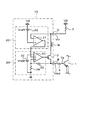
以下、本発明の第1実施形態について、図1〜図3を参照して説明する。
電気的構成を示す図1において、ゲート駆動回路10は、ゲート駆動形スイッチング素子としてのIGBT1を駆動するものである。ゲート駆動回路10は、入力端子Aに直流電源VDから電流検出用のシャント抵抗2を介して給電され、出力素子としてのPチャンネル型のMOSFET3のソース−ドレイン間を介して出力端子Bにゲート駆動信号を出力する。出力端子Bはゲート抵抗4を介してIGBT1のゲートに接続される。
電力変換装置200において、直流電源部201は、電動発電機100を回転駆動させる場合には、IGBT43および44をオンオフ制御することにより、バッテリ40の端子電圧を昇圧コイル42により昇圧させてコンデンサ45に充電する。三相インバータ202では、コンデンサ45を直流電源としてIGBT1a〜1fをそれぞれの駆動回路10a〜10fによりオンオフ駆動され、三相交流を生成して電動発電機100に給電する。
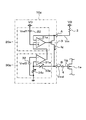
図4は第2実施形態を示すもので、以下、第1実施形態と異なる部分について説明する。この実施形態では、ゲート駆動回路10aは、定電流駆動回路20aおよび定電圧駆動回路30aを備え、MOSFET3のゲートに対して定電流駆動回路20aによりゲート信号を出力する構成である。
この結果、このような第2実施形態によっても第1実施形態と同様の作用効果を得ることができる。
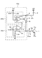
図5は第3実施形態を示すもので、以下、第1実施形態と異なる部分について説明する。この実施形態では、MOSFET3は、ソースが入力端子Aを介して直流電源VDに直接接続され、ドレインはシャント抵抗2を介して出力端子Bに接続されている。
したがって、このような第3実施形態によっても第1実施形態と同様の作用効果をえることができる。
図6は第4実施形態を示すもので、以下、第3実施形態と異なる部分について説明する。この実施形態では、第3実施形態のシャント抵抗2を省略し、ゲート電流Igの検出をゲート抵抗4により行う構成としている。
図7は第5実施形態を示すもので、以下、第2実施形態と異なる部分について説明する。この実施形態では、ゲート駆動回路10aは、第2実施形態と同様の構成を採用している。また、制御対象となるゲート駆動形スイッチング素子としてIGBT1に代えてnチャンネル型のMOSFET1aを駆動する構成である。
したがって、このような第5実施形態によっても、第2実施形態と同様の作用効果を得ることができる。
図8および図9は第6実施形態を示すもので、以下、第5実施形態と異なる部分について説明する。第6実施形態においては、図8および図9のそれぞれの定電流駆動制御において、定電流Igの値を設定変更することができる構成を採用している。
図10および図11は第7実施形態を示すもので、以下、第5実施形態と異なる部分について説明する。第7実施形態においては、図10および図11のそれぞれの定電圧駆動制御において、定電圧Vgの値を設定変更することができる構成を採用している。
なお、本発明は、上述した実施形態のみに限定されるものではなく、その要旨を逸脱しない範囲で種々の実施形態に適用可能であり、例えば、以下のように変形または拡張することができる。
第1〜第7実施形態は、互いに適宜組み合わせた複合的なゲート駆動回路を構成することができる。
Claims (7)
- ゲート駆動形スイッチング素子(1、1a)のゲートにゲート駆動信号を与える一つのみの出力素子(3)と、
前記ゲート駆動形スイッチング素子のゲートに前記ゲート駆動信号を定電流で与えるように前記出力素子を制御する定電流駆動回路(20、20a、20b、20c、20x)と、
前記ゲート駆動形スイッチング素子のゲートに前記ゲート駆動信号を定電圧で与えるように前記出力素子を制御する定電圧駆動回路(30、30a、30b、30c、30y、30z)とを備えたゲート駆動回路。 - 前記定電流駆動回路および前記定電圧駆動回路は、いずれか一方の出力が前記出力素子に与えられ、他方の出力が前記一方の入力として与えられるように接続される請求項1に記載のゲート駆動回路。
- 前記定電流駆動回路は、前記ゲート駆動形スイッチング素子に対して、ゲート電圧を所定の定電圧に達するまで定電流により一定の電圧上昇率で上昇させ、
前記定電圧駆動回路は、前記ゲート駆動形スイッチング素子に対して、ゲート電圧が所定の定電圧に達した後は定電圧で保持するように駆動制御される請求項2に記載のゲート駆動回路。 - 前記定電流駆動回路は、
第1参照電圧を発生させる第1参照電源(22、22x)と、
電源から前記出力素子に至る経路に設けられるシャント抵抗(2、2x)と、
前記シャント抵抗と前記出力素子との間の電圧が前記第1参照電圧に近づくように前記出力素子を制御し、前記出力素子に前記シャント抵抗の抵抗値と前記第1参照電圧とによって決まるシャント電流を流すように制御する第1差動アンプ(21、21a)とを備えた請求項1から3のいずれか一項に記載のゲート駆動回路。 - 前記定電圧駆動回路は、
第2参照電圧を発生させる第2参照電源(32、32y)と、
前記ゲート駆動形スイッチング素子のゲート電圧が前記第2参照電圧に近づくように前記出力素子を制御する第2差動アンプ(31、31a)とを備えた請求項1から4のいずれか一項に記載のゲート駆動回路。 - 前記定電流駆動回路(20a、20x)は、前記出力素子の前記シャント電流値を調整可能に設けられる請求項1から5のいずれか一項に記載のゲート駆動回路。
- 前記定電圧駆動回路(30y、30z)は、前記ゲート駆動形スイッチング素子に与えるゲート電圧を調整可能に設けられる請求項1から6のいずれか一項に記載のゲート駆動回路。
Priority Applications (3)
| Application Number | Priority Date | Filing Date | Title |
|---|---|---|---|
| JP2018230804A JP6962308B2 (ja) | 2018-12-10 | 2018-12-10 | ゲート駆動回路 |
| PCT/JP2019/044705 WO2020121727A1 (ja) | 2018-12-10 | 2019-11-14 | ゲート駆動回路 |
| US17/336,980 US11368147B2 (en) | 2018-12-10 | 2021-06-02 | Gate drive circuit |
Applications Claiming Priority (1)
| Application Number | Priority Date | Filing Date | Title |
|---|---|---|---|
| JP2018230804A JP6962308B2 (ja) | 2018-12-10 | 2018-12-10 | ゲート駆動回路 |
Publications (3)
| Publication Number | Publication Date |
|---|---|
| JP2020096222A JP2020096222A (ja) | 2020-06-18 |
| JP2020096222A5 JP2020096222A5 (ja) | 2020-11-12 |
| JP6962308B2 true JP6962308B2 (ja) | 2021-11-05 |
Family
ID=71076877
Family Applications (1)
| Application Number | Title | Priority Date | Filing Date |
|---|---|---|---|
| JP2018230804A Active JP6962308B2 (ja) | 2018-12-10 | 2018-12-10 | ゲート駆動回路 |
Country Status (3)
| Country | Link |
|---|---|
| US (1) | US11368147B2 (ja) |
| JP (1) | JP6962308B2 (ja) |
| WO (1) | WO2020121727A1 (ja) |
Families Citing this family (1)
| Publication number | Priority date | Publication date | Assignee | Title |
|---|---|---|---|---|
| JP2022093994A (ja) * | 2020-12-14 | 2022-06-24 | 株式会社東芝 | 電力変換装置 |
Family Cites Families (4)
| Publication number | Priority date | Publication date | Assignee | Title |
|---|---|---|---|---|
| JP5138287B2 (ja) | 2007-06-27 | 2013-02-06 | 三菱電機株式会社 | ゲート駆動装置 |
| JP5701176B2 (ja) * | 2011-08-04 | 2015-04-15 | 三菱電機株式会社 | ゲート駆動装置 |
| JP5761215B2 (ja) * | 2013-01-21 | 2015-08-12 | 株式会社デンソー | ゲート駆動回路 |
| CN103138573B (zh) * | 2013-02-28 | 2016-03-09 | 上海新进半导体制造有限公司 | 降压式开关电源及其控制电路 |
-
2018
- 2018-12-10 JP JP2018230804A patent/JP6962308B2/ja active Active
-
2019
- 2019-11-14 WO PCT/JP2019/044705 patent/WO2020121727A1/ja active Application Filing
-
2021
- 2021-06-02 US US17/336,980 patent/US11368147B2/en active Active
Also Published As
| Publication number | Publication date |
|---|---|
| JP2020096222A (ja) | 2020-06-18 |
| WO2020121727A1 (ja) | 2020-06-18 |
| US11368147B2 (en) | 2022-06-21 |
| US20210288639A1 (en) | 2021-09-16 |
Similar Documents
| Publication | Publication Date | Title |
|---|---|---|
| US9847779B2 (en) | Dead time adjusting circuit | |
| US8704556B2 (en) | Integrated circuit-based drive circuit for driving voltage-controlled switching device and method of manufacturing the drive circuit | |
| US20080024099A1 (en) | Power Supply Apparatus | |
| JP6597508B2 (ja) | 電力変換装置 | |
| US10122255B2 (en) | Devices, systems and processes for average current control | |
| US9923557B2 (en) | Switching circuit and power conversion circuit | |
| US9490705B2 (en) | Inverter device and air conditioner | |
| US11569654B2 (en) | Power control device | |
| CN108123623B (zh) | 整流器以及使用了该整流器的交流发电机 | |
| JP2019062714A (ja) | 同期整流回路及びスイッチング電源装置 | |
| JP2018129910A (ja) | Dc/dcコンバータおよびその制御回路、制御方法、車載電装機器 | |
| JP5077030B2 (ja) | モータ駆動回路およびモータの異常判定方法 | |
| JP6962308B2 (ja) | ゲート駆動回路 | |
| JP5864561B2 (ja) | 入力電流制限能力を有するスイッチングレギュレータ | |
| JP2016212005A (ja) | 電流検出装置 | |
| JP6139422B2 (ja) | 基準電圧出力回路および電源装置 | |
| EP3721540A1 (en) | Buck-boost power converter controller | |
| JP2005110366A (ja) | ドライブ回路 | |
| JP6642074B2 (ja) | スイッチング素子の駆動装置 | |
| JP6528611B2 (ja) | 制御回路およびスイッチング電源装置 | |
| JP6432412B2 (ja) | スイッチング素子の駆動装置 | |
| JP5500283B2 (ja) | スイッチング素子の駆動回路およびその製造方法 | |
| JP2022095502A (ja) | 充放電試験装置 | |
| JP2009165322A (ja) | 電源装置 |
Legal Events
| Date | Code | Title | Description |
|---|---|---|---|
| A521 | Request for written amendment filed |
Free format text: JAPANESE INTERMEDIATE CODE: A523 Effective date: 20200928 |
|
| A621 | Written request for application examination |
Free format text: JAPANESE INTERMEDIATE CODE: A621 Effective date: 20200928 |
|
| A131 | Notification of reasons for refusal |
Free format text: JAPANESE INTERMEDIATE CODE: A131 Effective date: 20201117 |
|
| A521 | Request for written amendment filed |
Free format text: JAPANESE INTERMEDIATE CODE: A523 Effective date: 20210112 |
|
| A131 | Notification of reasons for refusal |
Free format text: JAPANESE INTERMEDIATE CODE: A131 Effective date: 20210518 |
|
| A521 | Request for written amendment filed |
Free format text: JAPANESE INTERMEDIATE CODE: A523 Effective date: 20210706 |
|
| TRDD | Decision of grant or rejection written | ||
| A01 | Written decision to grant a patent or to grant a registration (utility model) |
Free format text: JAPANESE INTERMEDIATE CODE: A01 Effective date: 20210914 |
|
| A61 | First payment of annual fees (during grant procedure) |
Free format text: JAPANESE INTERMEDIATE CODE: A61 Effective date: 20210927 |
|
| R151 | Written notification of patent or utility model registration |
Ref document number: 6962308 Country of ref document: JP Free format text: JAPANESE INTERMEDIATE CODE: R151 |