JP6913569B2 - 被処理体を処理する方法 - Google Patents
被処理体を処理する方法 Download PDFInfo
- Publication number
- JP6913569B2 JP6913569B2 JP2017162600A JP2017162600A JP6913569B2 JP 6913569 B2 JP6913569 B2 JP 6913569B2 JP 2017162600 A JP2017162600 A JP 2017162600A JP 2017162600 A JP2017162600 A JP 2017162600A JP 6913569 B2 JP6913569 B2 JP 6913569B2
- Authority
- JP
- Japan
- Prior art keywords
- film
- gas
- hole
- etching
- processing
- Prior art date
- Legal status (The legal status is an assumption and is not a legal conclusion. Google has not performed a legal analysis and makes no representation as to the accuracy of the status listed.)
- Active
Links
Images


Classifications
-
- H—ELECTRICITY
- H01—ELECTRIC ELEMENTS
- H01L—SEMICONDUCTOR DEVICES NOT COVERED BY CLASS H10
- H01L21/00—Processes or apparatus adapted for the manufacture or treatment of semiconductor or solid state devices or of parts thereof
- H01L21/02—Manufacture or treatment of semiconductor devices or of parts thereof
- H01L21/027—Making masks on semiconductor bodies for further photolithographic processing not provided for in group H01L21/18 or H01L21/34
- H01L21/033—Making masks on semiconductor bodies for further photolithographic processing not provided for in group H01L21/18 or H01L21/34 comprising inorganic layers
- H01L21/0334—Making masks on semiconductor bodies for further photolithographic processing not provided for in group H01L21/18 or H01L21/34 comprising inorganic layers characterised by their size, orientation, disposition, behaviour, shape, in horizontal or vertical plane
- H01L21/0338—Process specially adapted to improve the resolution of the mask
-
- H—ELECTRICITY
- H01—ELECTRIC ELEMENTS
- H01J—ELECTRIC DISCHARGE TUBES OR DISCHARGE LAMPS
- H01J37/00—Discharge tubes with provision for introducing objects or material to be exposed to the discharge, e.g. for the purpose of examination or processing thereof
- H01J37/32—Gas-filled discharge tubes
- H01J37/32009—Arrangements for generation of plasma specially adapted for examination or treatment of objects, e.g. plasma sources
- H01J37/32082—Radio frequency generated discharge
- H01J37/321—Radio frequency generated discharge the radio frequency energy being inductively coupled to the plasma
- H01J37/3211—Antennas, e.g. particular shapes of coils
-
- H—ELECTRICITY
- H01—ELECTRIC ELEMENTS
- H01L—SEMICONDUCTOR DEVICES NOT COVERED BY CLASS H10
- H01L21/00—Processes or apparatus adapted for the manufacture or treatment of semiconductor or solid state devices or of parts thereof
- H01L21/02—Manufacture or treatment of semiconductor devices or of parts thereof
- H01L21/04—Manufacture or treatment of semiconductor devices or of parts thereof the devices having at least one potential-jump barrier or surface barrier, e.g. PN junction, depletion layer or carrier concentration layer
- H01L21/18—Manufacture or treatment of semiconductor devices or of parts thereof the devices having at least one potential-jump barrier or surface barrier, e.g. PN junction, depletion layer or carrier concentration layer the devices having semiconductor bodies comprising elements of Group IV of the Periodic System or AIIIBV compounds with or without impurities, e.g. doping materials
- H01L21/30—Treatment of semiconductor bodies using processes or apparatus not provided for in groups H01L21/20 - H01L21/26
- H01L21/302—Treatment of semiconductor bodies using processes or apparatus not provided for in groups H01L21/20 - H01L21/26 to change their surface-physical characteristics or shape, e.g. etching, polishing, cutting
- H01L21/306—Chemical or electrical treatment, e.g. electrolytic etching
- H01L21/3065—Plasma etching; Reactive-ion etching
-
- H—ELECTRICITY
- H01—ELECTRIC ELEMENTS
- H01J—ELECTRIC DISCHARGE TUBES OR DISCHARGE LAMPS
- H01J37/00—Discharge tubes with provision for introducing objects or material to be exposed to the discharge, e.g. for the purpose of examination or processing thereof
- H01J37/32—Gas-filled discharge tubes
- H01J37/32431—Constructional details of the reactor
- H01J37/3244—Gas supply means
-
- H—ELECTRICITY
- H01—ELECTRIC ELEMENTS
- H01J—ELECTRIC DISCHARGE TUBES OR DISCHARGE LAMPS
- H01J37/00—Discharge tubes with provision for introducing objects or material to be exposed to the discharge, e.g. for the purpose of examination or processing thereof
- H01J37/32—Gas-filled discharge tubes
- H01J37/32431—Constructional details of the reactor
- H01J37/32458—Vessel
-
- H—ELECTRICITY
- H01—ELECTRIC ELEMENTS
- H01J—ELECTRIC DISCHARGE TUBES OR DISCHARGE LAMPS
- H01J37/00—Discharge tubes with provision for introducing objects or material to be exposed to the discharge, e.g. for the purpose of examination or processing thereof
- H01J37/32—Gas-filled discharge tubes
- H01J37/32431—Constructional details of the reactor
- H01J37/32715—Workpiece holder
- H01J37/32724—Temperature
-
- H—ELECTRICITY
- H01—ELECTRIC ELEMENTS
- H01L—SEMICONDUCTOR DEVICES NOT COVERED BY CLASS H10
- H01L21/00—Processes or apparatus adapted for the manufacture or treatment of semiconductor or solid state devices or of parts thereof
- H01L21/02—Manufacture or treatment of semiconductor devices or of parts thereof
- H01L21/02104—Forming layers
- H01L21/02107—Forming insulating materials on a substrate
- H01L21/02109—Forming insulating materials on a substrate characterised by the type of layer, e.g. type of material, porous/non-porous, pre-cursors, mixtures or laminates
- H01L21/022—Forming insulating materials on a substrate characterised by the type of layer, e.g. type of material, porous/non-porous, pre-cursors, mixtures or laminates the layer being a laminate, i.e. composed of sublayers, e.g. stacks of alternating high-k metal oxides
-
- H—ELECTRICITY
- H01—ELECTRIC ELEMENTS
- H01L—SEMICONDUCTOR DEVICES NOT COVERED BY CLASS H10
- H01L21/00—Processes or apparatus adapted for the manufacture or treatment of semiconductor or solid state devices or of parts thereof
- H01L21/02—Manufacture or treatment of semiconductor devices or of parts thereof
- H01L21/02104—Forming layers
- H01L21/02107—Forming insulating materials on a substrate
- H01L21/02109—Forming insulating materials on a substrate characterised by the type of layer, e.g. type of material, porous/non-porous, pre-cursors, mixtures or laminates
- H01L21/02205—Forming insulating materials on a substrate characterised by the type of layer, e.g. type of material, porous/non-porous, pre-cursors, mixtures or laminates the layer being characterised by the precursor material for deposition
- H01L21/02208—Forming insulating materials on a substrate characterised by the type of layer, e.g. type of material, porous/non-porous, pre-cursors, mixtures or laminates the layer being characterised by the precursor material for deposition the precursor containing a compound comprising Si
- H01L21/02211—Forming insulating materials on a substrate characterised by the type of layer, e.g. type of material, porous/non-porous, pre-cursors, mixtures or laminates the layer being characterised by the precursor material for deposition the precursor containing a compound comprising Si the compound being a silane, e.g. disilane, methylsilane or chlorosilane
-
- H—ELECTRICITY
- H01—ELECTRIC ELEMENTS
- H01L—SEMICONDUCTOR DEVICES NOT COVERED BY CLASS H10
- H01L21/00—Processes or apparatus adapted for the manufacture or treatment of semiconductor or solid state devices or of parts thereof
- H01L21/02—Manufacture or treatment of semiconductor devices or of parts thereof
- H01L21/02104—Forming layers
- H01L21/02107—Forming insulating materials on a substrate
- H01L21/02109—Forming insulating materials on a substrate characterised by the type of layer, e.g. type of material, porous/non-porous, pre-cursors, mixtures or laminates
- H01L21/02205—Forming insulating materials on a substrate characterised by the type of layer, e.g. type of material, porous/non-porous, pre-cursors, mixtures or laminates the layer being characterised by the precursor material for deposition
- H01L21/02208—Forming insulating materials on a substrate characterised by the type of layer, e.g. type of material, porous/non-porous, pre-cursors, mixtures or laminates the layer being characterised by the precursor material for deposition the precursor containing a compound comprising Si
- H01L21/02219—Forming insulating materials on a substrate characterised by the type of layer, e.g. type of material, porous/non-porous, pre-cursors, mixtures or laminates the layer being characterised by the precursor material for deposition the precursor containing a compound comprising Si the compound comprising silicon and nitrogen
-
- H—ELECTRICITY
- H01—ELECTRIC ELEMENTS
- H01L—SEMICONDUCTOR DEVICES NOT COVERED BY CLASS H10
- H01L21/00—Processes or apparatus adapted for the manufacture or treatment of semiconductor or solid state devices or of parts thereof
- H01L21/02—Manufacture or treatment of semiconductor devices or of parts thereof
- H01L21/02104—Forming layers
- H01L21/02107—Forming insulating materials on a substrate
- H01L21/02225—Forming insulating materials on a substrate characterised by the process for the formation of the insulating layer
- H01L21/0226—Forming insulating materials on a substrate characterised by the process for the formation of the insulating layer formation by a deposition process
- H01L21/02263—Forming insulating materials on a substrate characterised by the process for the formation of the insulating layer formation by a deposition process deposition from the gas or vapour phase
- H01L21/02271—Forming insulating materials on a substrate characterised by the process for the formation of the insulating layer formation by a deposition process deposition from the gas or vapour phase deposition by decomposition or reaction of gaseous or vapour phase compounds, i.e. chemical vapour deposition
- H01L21/02274—Forming insulating materials on a substrate characterised by the process for the formation of the insulating layer formation by a deposition process deposition from the gas or vapour phase deposition by decomposition or reaction of gaseous or vapour phase compounds, i.e. chemical vapour deposition in the presence of a plasma [PECVD]
-
- H—ELECTRICITY
- H01—ELECTRIC ELEMENTS
- H01L—SEMICONDUCTOR DEVICES NOT COVERED BY CLASS H10
- H01L21/00—Processes or apparatus adapted for the manufacture or treatment of semiconductor or solid state devices or of parts thereof
- H01L21/02—Manufacture or treatment of semiconductor devices or of parts thereof
- H01L21/02104—Forming layers
- H01L21/02107—Forming insulating materials on a substrate
- H01L21/02225—Forming insulating materials on a substrate characterised by the process for the formation of the insulating layer
- H01L21/0226—Forming insulating materials on a substrate characterised by the process for the formation of the insulating layer formation by a deposition process
- H01L21/02263—Forming insulating materials on a substrate characterised by the process for the formation of the insulating layer formation by a deposition process deposition from the gas or vapour phase
- H01L21/02271—Forming insulating materials on a substrate characterised by the process for the formation of the insulating layer formation by a deposition process deposition from the gas or vapour phase deposition by decomposition or reaction of gaseous or vapour phase compounds, i.e. chemical vapour deposition
- H01L21/0228—Forming insulating materials on a substrate characterised by the process for the formation of the insulating layer formation by a deposition process deposition from the gas or vapour phase deposition by decomposition or reaction of gaseous or vapour phase compounds, i.e. chemical vapour deposition deposition by cyclic CVD, e.g. ALD, ALE, pulsed CVD
-
- H—ELECTRICITY
- H01—ELECTRIC ELEMENTS
- H01L—SEMICONDUCTOR DEVICES NOT COVERED BY CLASS H10
- H01L21/00—Processes or apparatus adapted for the manufacture or treatment of semiconductor or solid state devices or of parts thereof
- H01L21/02—Manufacture or treatment of semiconductor devices or of parts thereof
- H01L21/02104—Forming layers
- H01L21/02107—Forming insulating materials on a substrate
- H01L21/02296—Forming insulating materials on a substrate characterised by the treatment performed before or after the formation of the layer
- H01L21/02318—Forming insulating materials on a substrate characterised by the treatment performed before or after the formation of the layer post-treatment
- H01L21/02321—Forming insulating materials on a substrate characterised by the treatment performed before or after the formation of the layer post-treatment introduction of substances into an already existing insulating layer
- H01L21/02329—Forming insulating materials on a substrate characterised by the treatment performed before or after the formation of the layer post-treatment introduction of substances into an already existing insulating layer introduction of nitrogen
- H01L21/02332—Forming insulating materials on a substrate characterised by the treatment performed before or after the formation of the layer post-treatment introduction of substances into an already existing insulating layer introduction of nitrogen into an oxide layer, e.g. changing SiO to SiON
-
- H—ELECTRICITY
- H01—ELECTRIC ELEMENTS
- H01L—SEMICONDUCTOR DEVICES NOT COVERED BY CLASS H10
- H01L21/00—Processes or apparatus adapted for the manufacture or treatment of semiconductor or solid state devices or of parts thereof
- H01L21/02—Manufacture or treatment of semiconductor devices or of parts thereof
- H01L21/02104—Forming layers
- H01L21/02107—Forming insulating materials on a substrate
- H01L21/02296—Forming insulating materials on a substrate characterised by the treatment performed before or after the formation of the layer
- H01L21/02318—Forming insulating materials on a substrate characterised by the treatment performed before or after the formation of the layer post-treatment
- H01L21/02337—Forming insulating materials on a substrate characterised by the treatment performed before or after the formation of the layer post-treatment treatment by exposure to a gas or vapour
- H01L21/0234—Forming insulating materials on a substrate characterised by the treatment performed before or after the formation of the layer post-treatment treatment by exposure to a gas or vapour treatment by exposure to a plasma
-
- H—ELECTRICITY
- H01—ELECTRIC ELEMENTS
- H01L—SEMICONDUCTOR DEVICES NOT COVERED BY CLASS H10
- H01L21/00—Processes or apparatus adapted for the manufacture or treatment of semiconductor or solid state devices or of parts thereof
- H01L21/02—Manufacture or treatment of semiconductor devices or of parts thereof
- H01L21/027—Making masks on semiconductor bodies for further photolithographic processing not provided for in group H01L21/18 or H01L21/34
- H01L21/0271—Making masks on semiconductor bodies for further photolithographic processing not provided for in group H01L21/18 or H01L21/34 comprising organic layers
- H01L21/0273—Making masks on semiconductor bodies for further photolithographic processing not provided for in group H01L21/18 or H01L21/34 comprising organic layers characterised by the treatment of photoresist layers
- H01L21/0274—Photolithographic processes
-
- H—ELECTRICITY
- H01—ELECTRIC ELEMENTS
- H01L—SEMICONDUCTOR DEVICES NOT COVERED BY CLASS H10
- H01L21/00—Processes or apparatus adapted for the manufacture or treatment of semiconductor or solid state devices or of parts thereof
- H01L21/02—Manufacture or treatment of semiconductor devices or of parts thereof
- H01L21/027—Making masks on semiconductor bodies for further photolithographic processing not provided for in group H01L21/18 or H01L21/34
- H01L21/033—Making masks on semiconductor bodies for further photolithographic processing not provided for in group H01L21/18 or H01L21/34 comprising inorganic layers
- H01L21/0334—Making masks on semiconductor bodies for further photolithographic processing not provided for in group H01L21/18 or H01L21/34 comprising inorganic layers characterised by their size, orientation, disposition, behaviour, shape, in horizontal or vertical plane
- H01L21/0337—Making masks on semiconductor bodies for further photolithographic processing not provided for in group H01L21/18 or H01L21/34 comprising inorganic layers characterised by their size, orientation, disposition, behaviour, shape, in horizontal or vertical plane characterised by the process involved to create the mask, e.g. lift-off masks, sidewalls, or to modify the mask, e.g. pre-treatment, post-treatment
-
- H—ELECTRICITY
- H01—ELECTRIC ELEMENTS
- H01L—SEMICONDUCTOR DEVICES NOT COVERED BY CLASS H10
- H01L21/00—Processes or apparatus adapted for the manufacture or treatment of semiconductor or solid state devices or of parts thereof
- H01L21/02—Manufacture or treatment of semiconductor devices or of parts thereof
- H01L21/04—Manufacture or treatment of semiconductor devices or of parts thereof the devices having at least one potential-jump barrier or surface barrier, e.g. PN junction, depletion layer or carrier concentration layer
- H01L21/18—Manufacture or treatment of semiconductor devices or of parts thereof the devices having at least one potential-jump barrier or surface barrier, e.g. PN junction, depletion layer or carrier concentration layer the devices having semiconductor bodies comprising elements of Group IV of the Periodic System or AIIIBV compounds with or without impurities, e.g. doping materials
- H01L21/30—Treatment of semiconductor bodies using processes or apparatus not provided for in groups H01L21/20 - H01L21/26
- H01L21/302—Treatment of semiconductor bodies using processes or apparatus not provided for in groups H01L21/20 - H01L21/26 to change their surface-physical characteristics or shape, e.g. etching, polishing, cutting
- H01L21/306—Chemical or electrical treatment, e.g. electrolytic etching
- H01L21/308—Chemical or electrical treatment, e.g. electrolytic etching using masks
- H01L21/3083—Chemical or electrical treatment, e.g. electrolytic etching using masks characterised by their size, orientation, disposition, behaviour, shape, in horizontal or vertical plane
- H01L21/3088—Process specially adapted to improve the resolution of the mask
-
- H—ELECTRICITY
- H01—ELECTRIC ELEMENTS
- H01L—SEMICONDUCTOR DEVICES NOT COVERED BY CLASS H10
- H01L21/00—Processes or apparatus adapted for the manufacture or treatment of semiconductor or solid state devices or of parts thereof
- H01L21/02—Manufacture or treatment of semiconductor devices or of parts thereof
- H01L21/04—Manufacture or treatment of semiconductor devices or of parts thereof the devices having at least one potential-jump barrier or surface barrier, e.g. PN junction, depletion layer or carrier concentration layer
- H01L21/18—Manufacture or treatment of semiconductor devices or of parts thereof the devices having at least one potential-jump barrier or surface barrier, e.g. PN junction, depletion layer or carrier concentration layer the devices having semiconductor bodies comprising elements of Group IV of the Periodic System or AIIIBV compounds with or without impurities, e.g. doping materials
- H01L21/30—Treatment of semiconductor bodies using processes or apparatus not provided for in groups H01L21/20 - H01L21/26
- H01L21/31—Treatment of semiconductor bodies using processes or apparatus not provided for in groups H01L21/20 - H01L21/26 to form insulating layers thereon, e.g. for masking or by using photolithographic techniques; After treatment of these layers; Selection of materials for these layers
- H01L21/3105—After-treatment
- H01L21/311—Etching the insulating layers by chemical or physical means
- H01L21/31105—Etching inorganic layers
- H01L21/31111—Etching inorganic layers by chemical means
- H01L21/31116—Etching inorganic layers by chemical means by dry-etching
-
- H—ELECTRICITY
- H01—ELECTRIC ELEMENTS
- H01L—SEMICONDUCTOR DEVICES NOT COVERED BY CLASS H10
- H01L21/00—Processes or apparatus adapted for the manufacture or treatment of semiconductor or solid state devices or of parts thereof
- H01L21/02—Manufacture or treatment of semiconductor devices or of parts thereof
- H01L21/04—Manufacture or treatment of semiconductor devices or of parts thereof the devices having at least one potential-jump barrier or surface barrier, e.g. PN junction, depletion layer or carrier concentration layer
- H01L21/18—Manufacture or treatment of semiconductor devices or of parts thereof the devices having at least one potential-jump barrier or surface barrier, e.g. PN junction, depletion layer or carrier concentration layer the devices having semiconductor bodies comprising elements of Group IV of the Periodic System or AIIIBV compounds with or without impurities, e.g. doping materials
- H01L21/30—Treatment of semiconductor bodies using processes or apparatus not provided for in groups H01L21/20 - H01L21/26
- H01L21/31—Treatment of semiconductor bodies using processes or apparatus not provided for in groups H01L21/20 - H01L21/26 to form insulating layers thereon, e.g. for masking or by using photolithographic techniques; After treatment of these layers; Selection of materials for these layers
- H01L21/3105—After-treatment
- H01L21/311—Etching the insulating layers by chemical or physical means
- H01L21/31144—Etching the insulating layers by chemical or physical means using masks
-
- H—ELECTRICITY
- H01—ELECTRIC ELEMENTS
- H01L—SEMICONDUCTOR DEVICES NOT COVERED BY CLASS H10
- H01L21/00—Processes or apparatus adapted for the manufacture or treatment of semiconductor or solid state devices or of parts thereof
- H01L21/02—Manufacture or treatment of semiconductor devices or of parts thereof
- H01L21/04—Manufacture or treatment of semiconductor devices or of parts thereof the devices having at least one potential-jump barrier or surface barrier, e.g. PN junction, depletion layer or carrier concentration layer
- H01L21/18—Manufacture or treatment of semiconductor devices or of parts thereof the devices having at least one potential-jump barrier or surface barrier, e.g. PN junction, depletion layer or carrier concentration layer the devices having semiconductor bodies comprising elements of Group IV of the Periodic System or AIIIBV compounds with or without impurities, e.g. doping materials
- H01L21/30—Treatment of semiconductor bodies using processes or apparatus not provided for in groups H01L21/20 - H01L21/26
- H01L21/31—Treatment of semiconductor bodies using processes or apparatus not provided for in groups H01L21/20 - H01L21/26 to form insulating layers thereon, e.g. for masking or by using photolithographic techniques; After treatment of these layers; Selection of materials for these layers
- H01L21/3205—Deposition of non-insulating-, e.g. conductive- or resistive-, layers on insulating layers; After-treatment of these layers
- H01L21/321—After treatment
- H01L21/3213—Physical or chemical etching of the layers, e.g. to produce a patterned layer from a pre-deposited extensive layer
- H01L21/32133—Physical or chemical etching of the layers, e.g. to produce a patterned layer from a pre-deposited extensive layer by chemical means only
- H01L21/32135—Physical or chemical etching of the layers, e.g. to produce a patterned layer from a pre-deposited extensive layer by chemical means only by vapour etching only
- H01L21/32136—Physical or chemical etching of the layers, e.g. to produce a patterned layer from a pre-deposited extensive layer by chemical means only by vapour etching only using plasmas
-
- H—ELECTRICITY
- H01—ELECTRIC ELEMENTS
- H01L—SEMICONDUCTOR DEVICES NOT COVERED BY CLASS H10
- H01L21/00—Processes or apparatus adapted for the manufacture or treatment of semiconductor or solid state devices or of parts thereof
- H01L21/67—Apparatus specially adapted for handling semiconductor or electric solid state devices during manufacture or treatment thereof; Apparatus specially adapted for handling wafers during manufacture or treatment of semiconductor or electric solid state devices or components ; Apparatus not specifically provided for elsewhere
- H01L21/67005—Apparatus not specifically provided for elsewhere
- H01L21/67011—Apparatus for manufacture or treatment
- H01L21/67098—Apparatus for thermal treatment
- H01L21/67109—Apparatus for thermal treatment mainly by convection
-
- H—ELECTRICITY
- H01—ELECTRIC ELEMENTS
- H01L—SEMICONDUCTOR DEVICES NOT COVERED BY CLASS H10
- H01L21/00—Processes or apparatus adapted for the manufacture or treatment of semiconductor or solid state devices or of parts thereof
- H01L21/67—Apparatus specially adapted for handling semiconductor or electric solid state devices during manufacture or treatment thereof; Apparatus specially adapted for handling wafers during manufacture or treatment of semiconductor or electric solid state devices or components ; Apparatus not specifically provided for elsewhere
- H01L21/67005—Apparatus not specifically provided for elsewhere
- H01L21/67242—Apparatus for monitoring, sorting or marking
- H01L21/67253—Process monitoring, e.g. flow or thickness monitoring
-
- H—ELECTRICITY
- H01—ELECTRIC ELEMENTS
- H01L—SEMICONDUCTOR DEVICES NOT COVERED BY CLASS H10
- H01L21/00—Processes or apparatus adapted for the manufacture or treatment of semiconductor or solid state devices or of parts thereof
- H01L21/67—Apparatus specially adapted for handling semiconductor or electric solid state devices during manufacture or treatment thereof; Apparatus specially adapted for handling wafers during manufacture or treatment of semiconductor or electric solid state devices or components ; Apparatus not specifically provided for elsewhere
- H01L21/683—Apparatus specially adapted for handling semiconductor or electric solid state devices during manufacture or treatment thereof; Apparatus specially adapted for handling wafers during manufacture or treatment of semiconductor or electric solid state devices or components ; Apparatus not specifically provided for elsewhere for supporting or gripping
- H01L21/6831—Apparatus specially adapted for handling semiconductor or electric solid state devices during manufacture or treatment thereof; Apparatus specially adapted for handling wafers during manufacture or treatment of semiconductor or electric solid state devices or components ; Apparatus not specifically provided for elsewhere for supporting or gripping using electrostatic chucks
- H01L21/6833—Details of electrostatic chucks
-
- H—ELECTRICITY
- H05—ELECTRIC TECHNIQUES NOT OTHERWISE PROVIDED FOR
- H05H—PLASMA TECHNIQUE; PRODUCTION OF ACCELERATED ELECTRICALLY-CHARGED PARTICLES OR OF NEUTRONS; PRODUCTION OR ACCELERATION OF NEUTRAL MOLECULAR OR ATOMIC BEAMS
- H05H1/00—Generating plasma; Handling plasma
- H05H1/24—Generating plasma
- H05H1/46—Generating plasma using applied electromagnetic fields, e.g. high frequency or microwave energy
-
- H—ELECTRICITY
- H01—ELECTRIC ELEMENTS
- H01J—ELECTRIC DISCHARGE TUBES OR DISCHARGE LAMPS
- H01J2237/00—Discharge tubes exposing object to beam, e.g. for analysis treatment, etching, imaging
- H01J2237/32—Processing objects by plasma generation
- H01J2237/33—Processing objects by plasma generation characterised by the type of processing
- H01J2237/334—Etching
- H01J2237/3341—Reactive etching
-
- H—ELECTRICITY
- H01—ELECTRIC ELEMENTS
- H01J—ELECTRIC DISCHARGE TUBES OR DISCHARGE LAMPS
- H01J2237/00—Discharge tubes exposing object to beam, e.g. for analysis treatment, etching, imaging
- H01J2237/32—Processing objects by plasma generation
- H01J2237/33—Processing objects by plasma generation characterised by the type of processing
- H01J2237/334—Etching
- H01J2237/3343—Problems associated with etching
- H01J2237/3344—Problems associated with etching isotropy
-
- H—ELECTRICITY
- H01—ELECTRIC ELEMENTS
- H01L—SEMICONDUCTOR DEVICES NOT COVERED BY CLASS H10
- H01L21/00—Processes or apparatus adapted for the manufacture or treatment of semiconductor or solid state devices or of parts thereof
- H01L21/02—Manufacture or treatment of semiconductor devices or of parts thereof
- H01L21/04—Manufacture or treatment of semiconductor devices or of parts thereof the devices having at least one potential-jump barrier or surface barrier, e.g. PN junction, depletion layer or carrier concentration layer
- H01L21/18—Manufacture or treatment of semiconductor devices or of parts thereof the devices having at least one potential-jump barrier or surface barrier, e.g. PN junction, depletion layer or carrier concentration layer the devices having semiconductor bodies comprising elements of Group IV of the Periodic System or AIIIBV compounds with or without impurities, e.g. doping materials
- H01L21/28—Manufacture of electrodes on semiconductor bodies using processes or apparatus not provided for in groups H01L21/20 - H01L21/268
- H01L21/28008—Making conductor-insulator-semiconductor electrodes
- H01L21/28017—Making conductor-insulator-semiconductor electrodes the insulator being formed after the semiconductor body, the semiconductor being silicon
- H01L21/28026—Making conductor-insulator-semiconductor electrodes the insulator being formed after the semiconductor body, the semiconductor being silicon characterised by the conductor
- H01L21/28123—Lithography-related aspects, e.g. sub-lithography lengths; Isolation-related aspects, e.g. to solve problems arising at the crossing with the side of the device isolation; Planarisation aspects
- H01L21/28132—Lithography-related aspects, e.g. sub-lithography lengths; Isolation-related aspects, e.g. to solve problems arising at the crossing with the side of the device isolation; Planarisation aspects conducting part of electrode is difined by a sidewall spacer or a similar technique, e.g. oxidation under mask, plating
Description
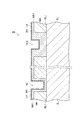
このように、第1シーケンスが繰り返し実行されるので、比較的に薄い膜厚の膜を第1工程において形成し第1シーケンスを繰り返し実行することによって最終的に所望とする膜厚の膜を形成することができる。これにより、ホール幅の比較的に狭いホールにおいて、第1工程によって形成される膜によってホールの開口が閉塞される事態が十分に回避され得る。
比較的にホール幅が狭く第1工程で比較的に膜厚の薄い膜が形成されたホール(第1ホールという)において第2の膜が第2工程で除去されても、この時点において、比較的にホール幅が広く第1工程で比較的に膜厚の厚い膜が形成されたホール(第2ホールという)では第2の膜の一部が残存し得る。このような状態から、第2工程におけるエッチングが更に継続して行われる場合、第1の膜のエッチング耐性が第2の膜のエッチング耐性よりも低いので、第1ホールの方が第2ホールよりも速くエッチングが進行する。従って、比較的にエッチング耐性の低い第1の膜と比較的にエッチング耐性の高い第2の膜とを用いることによって、第1ホールと第2ホールとの間のホール幅のバラツキがより効果的に低減され得る。
Claims (12)
- 被処理体を処理する方法であって、
複数のホールが表面に設けられた被処理体を提供する工程と、
プラズマCVDにより前記ホールの内面に膜を形成する工程と、
前記膜を等方的にエッチングする工程と、
を含み、
エッチングする前記工程は、
窒素を含む第1のガスからプラズマを生成し、前記ホールの内面に混合層を形成する工程と、
次いで、フッ素を含む第2のガスからプラズマを生成し、前記混合層を除去する工程と、
を繰り返して、前記膜を等方的にエッチングする、
方法。 - 膜を形成する前記工程とエッチングする前記工程とは、繰り返し実行される、
請求項1に記載の方法。 - 前記第2のガスは、NF3ガスおよびO2ガスを含む、
請求項1に記載の方法。 - 前記第2のガスは、NF3ガス、O2ガス、H2ガスおよびArガスを含む、
請求項1に記載の方法。 - 前記第2のガスは、CH3Fガス、O2ガスおよびArガスを含む、
請求項1に記載の方法。 - 膜を形成する前記工程は、
前記ホールの内面に第1の膜を形成する段階と、
前記第1の膜上に第2の膜を形成する段階と、
を備え、
エッチングする前記工程における前記第1の膜のエッチング耐性は、前記第2の膜のエッチング耐性よりも低い、
請求項1から5の何れか一項に記載の方法。 - 第1の膜を形成する前記段階は、
前記被処理体にアミノシラン系ガスを吸着させることと、
酸素を含むガスからプラズマを生成することと、を繰り返すこと、
を含み、
第2の膜を形成する前記段階は、プラズマCVDにより該第2の膜を形成する、
請求項6に記載の方法。 - 被処理体を処理する方法であって、
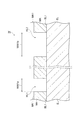
被処理体を提供する工程であって、該被処理体には複数のホールが表面に設けられており、該複数のホールは第1のホール幅を有する第1のホール及び該第1のホール幅よりも大きい第2のホール幅を有する第2のホールを含む、該工程と、
前記被処理体にシーケンスを実行する工程と、
を備え、
前記シーケンスは、
前記複数のホールのそれぞれの内面に膜を形成する工程であって、前記第1のホールに形成される該膜の厚さが前記第2のホールに形成される該膜の厚さよりも小さくなるように該膜を形成する、該工程と、
前記膜を等方的にエッチングする工程であって、該エッチング後における前記第1のホール幅と前記第2のホール幅との差は、膜を形成する前記工程の開始時における該第1のホール幅と該第2のホール幅との差よりも小さく、該エッチング後における該第1のホール幅及び該第2のホール幅のそれぞれは、膜を形成する該工程の開始時における該第1のホール幅及び該第2のホール幅のそれぞれよりも狭い、該工程と、
を含む、
方法。 - 被処理体を処理する方法であって、
被処理体を提供する工程であって、該被処理体には複数のホールが表面に設けられており、該複数のホールは第1のホール幅を有する第1のホール及び該第1のホール幅よりも大きい第2のホール幅を有する第2のホールを含む、該工程と、
前記被処理体にシーケンスを実行する工程と、
を備え、
前記シーケンスは、
前記複数のホールのそれぞれの内面に膜を形成する工程であって、前記第1のホールに形成される該膜の厚さが前記第2のホールに形成される該膜の厚さよりも小さくなるように該膜を形成する、該工程と、
前記膜を等方的にエッチングする工程であって、該エッチング後における前記第1のホール幅と前記第2のホール幅との差は、膜を形成する前記工程の開始時における該第1のホール幅と該第2のホール幅との差よりも小さい、該工程と、
を含む、
方法(ただし、前記エッチング後において相互に隣接するホール間の距離が前記被処理体内で均一になる場合を除く)。 - 膜を形成する前記工程は、プラズマCVDによる成膜処理を含む、
請求項8または9に記載の方法。 - 前記膜は、シリコンを含有する、
請求項8から10の何れか一項に記載の方法。 - 前記シーケンスは、繰り返し実行される、
請求項8から11の何れか一項に記載の方法。
Priority Applications (7)
| Application Number | Priority Date | Filing Date | Title |
|---|---|---|---|
| JP2017162600A JP6913569B2 (ja) | 2017-08-25 | 2017-08-25 | 被処理体を処理する方法 |
| TW107128535A TWI785095B (zh) | 2017-08-25 | 2018-08-16 | 被處理體之處理方法 |
| TW111137161A TW202305153A (zh) | 2017-08-25 | 2018-08-16 | 電漿處理裝置 |
| KR1020180098612A KR20190022389A (ko) | 2017-08-25 | 2018-08-23 | 피처리체를 처리하는 방법 |
| US16/111,622 US10559472B2 (en) | 2017-08-25 | 2018-08-24 | Workpiece processing method |
| CN201810971378.4A CN109427561B (zh) | 2017-08-25 | 2018-08-24 | 处理被处理体的方法 |
| US16/731,456 US11133192B2 (en) | 2017-08-25 | 2019-12-31 | Workpiece processing method |
Applications Claiming Priority (1)
| Application Number | Priority Date | Filing Date | Title |
|---|---|---|---|
| JP2017162600A JP6913569B2 (ja) | 2017-08-25 | 2017-08-25 | 被処理体を処理する方法 |
Publications (3)
| Publication Number | Publication Date |
|---|---|
| JP2019041020A JP2019041020A (ja) | 2019-03-14 |
| JP2019041020A5 JP2019041020A5 (ja) | 2020-06-18 |
| JP6913569B2 true JP6913569B2 (ja) | 2021-08-04 |
Family
ID=65437681
Family Applications (1)
| Application Number | Title | Priority Date | Filing Date |
|---|---|---|---|
| JP2017162600A Active JP6913569B2 (ja) | 2017-08-25 | 2017-08-25 | 被処理体を処理する方法 |
Country Status (5)
| Country | Link |
|---|---|
| US (2) | US10559472B2 (ja) |
| JP (1) | JP6913569B2 (ja) |
| KR (1) | KR20190022389A (ja) |
| CN (1) | CN109427561B (ja) |
| TW (2) | TW202305153A (ja) |
Families Citing this family (5)
| Publication number | Priority date | Publication date | Assignee | Title |
|---|---|---|---|---|
| JP7071175B2 (ja) * | 2017-04-18 | 2022-05-18 | 東京エレクトロン株式会社 | 被処理体を処理する方法 |
| JP7066565B2 (ja) * | 2018-07-27 | 2022-05-13 | 東京エレクトロン株式会社 | プラズマ処理方法およびプラズマ処理装置 |
| US10950428B1 (en) * | 2019-08-30 | 2021-03-16 | Mattson Technology, Inc. | Method for processing a workpiece |
| KR20220057624A (ko) * | 2019-09-12 | 2022-05-09 | 어플라이드 머티어리얼스, 인코포레이티드 | 반발 메시 및 증착 방법들 |
| JP2022029546A (ja) * | 2020-08-05 | 2022-02-18 | キオクシア株式会社 | 半導体記憶装置及びその製造方法 |
Family Cites Families (18)
| Publication number | Priority date | Publication date | Assignee | Title |
|---|---|---|---|---|
| US6635335B1 (en) * | 1999-06-29 | 2003-10-21 | Micron Technology, Inc. | Etching methods and apparatus and substrate assemblies produced therewith |
| JP4727171B2 (ja) * | 2003-09-29 | 2011-07-20 | 東京エレクトロン株式会社 | エッチング方法 |
| US7780865B2 (en) * | 2006-03-31 | 2010-08-24 | Applied Materials, Inc. | Method to improve the step coverage and pattern loading for dielectric films |
| US7524750B2 (en) * | 2006-04-17 | 2009-04-28 | Applied Materials, Inc. | Integrated process modulation (IPM) a novel solution for gapfill with HDP-CVD |
| JP5082338B2 (ja) * | 2006-08-25 | 2012-11-28 | 東京エレクトロン株式会社 | エッチング方法及びエッチング装置 |
| US8133797B2 (en) * | 2008-05-16 | 2012-03-13 | Novellus Systems, Inc. | Protective layer to enable damage free gap fill |
| JP2010283213A (ja) * | 2009-06-05 | 2010-12-16 | Tokyo Electron Ltd | 基板処理方法 |
| US8728956B2 (en) * | 2010-04-15 | 2014-05-20 | Novellus Systems, Inc. | Plasma activated conformal film deposition |
| JP2014003085A (ja) * | 2012-06-15 | 2014-01-09 | Tokyo Electron Ltd | プラズマエッチング方法及びプラズマ処理装置 |
| WO2014115600A1 (ja) * | 2013-01-22 | 2014-07-31 | ピーエスフォー ルクスコ エスエイアールエル | 半導体装置の製造方法 |
| US9378971B1 (en) * | 2014-12-04 | 2016-06-28 | Lam Research Corporation | Technique to deposit sidewall passivation for high aspect ratio cylinder etch |
| JP6207947B2 (ja) * | 2013-09-24 | 2017-10-04 | 東京エレクトロン株式会社 | 被処理体をプラズマ処理する方法 |
| US9190478B2 (en) * | 2013-12-22 | 2015-11-17 | Alpha And Omega Semiconductor Incorporated | Method for forming dual oxide trench gate power MOSFET using oxide filled trench |
| JP6151215B2 (ja) * | 2014-05-15 | 2017-06-21 | 東京エレクトロン株式会社 | プラズマエッチング方法 |
| JP2016058590A (ja) * | 2014-09-11 | 2016-04-21 | 株式会社日立ハイテクノロジーズ | プラズマ処理方法 |
| US9425041B2 (en) * | 2015-01-06 | 2016-08-23 | Lam Research Corporation | Isotropic atomic layer etch for silicon oxides using no activation |
| JP6559430B2 (ja) * | 2015-01-30 | 2019-08-14 | 東京エレクトロン株式会社 | 被処理体を処理する方法 |
| US9922839B2 (en) | 2015-06-23 | 2018-03-20 | Lam Research Corporation | Low roughness EUV lithography |
-
2017
- 2017-08-25 JP JP2017162600A patent/JP6913569B2/ja active Active
-
2018
- 2018-08-16 TW TW111137161A patent/TW202305153A/zh unknown
- 2018-08-16 TW TW107128535A patent/TWI785095B/zh active
- 2018-08-23 KR KR1020180098612A patent/KR20190022389A/ko not_active Application Discontinuation
- 2018-08-24 CN CN201810971378.4A patent/CN109427561B/zh active Active
- 2018-08-24 US US16/111,622 patent/US10559472B2/en active Active
-
2019
- 2019-12-31 US US16/731,456 patent/US11133192B2/en active Active
Also Published As
| Publication number | Publication date |
|---|---|
| CN109427561B (zh) | 2023-07-07 |
| TW202305153A (zh) | 2023-02-01 |
| TWI785095B (zh) | 2022-12-01 |
| TW201920716A (zh) | 2019-06-01 |
| US20200135480A1 (en) | 2020-04-30 |
| US10559472B2 (en) | 2020-02-11 |
| US11133192B2 (en) | 2021-09-28 |
| CN109427561A (zh) | 2019-03-05 |
| KR20190022389A (ko) | 2019-03-06 |
| US20190067019A1 (en) | 2019-02-28 |
| JP2019041020A (ja) | 2019-03-14 |
Similar Documents
| Publication | Publication Date | Title |
|---|---|---|
| JP6913569B2 (ja) | 被処理体を処理する方法 | |
| JP6759004B2 (ja) | 被処理体を処理する方法 | |
| CN108878285B (zh) | 蚀刻方法 | |
| KR20170041154A (ko) | 피처리체의 처리 방법 | |
| US11735423B2 (en) | Workpiece processing method | |
| US20210327719A1 (en) | Method for processing workpiece | |
| CN109417029B (zh) | 对被处理体进行处理的方法 | |
| TW201931465A (zh) | 電漿蝕刻方法及電漿蝕刻裝置 | |
| TWI830129B (zh) | 蝕刻裝置及蝕刻方法 | |
| JP7045428B2 (ja) | 被処理体を処理する方法 | |
| TWI836576B (zh) | 電漿處理裝置及電漿處理方法 |
Legal Events
| Date | Code | Title | Description |
|---|---|---|---|
| A521 | Request for written amendment filed |
Free format text: JAPANESE INTERMEDIATE CODE: A523 Effective date: 20200323 |
|
| A621 | Written request for application examination |
Free format text: JAPANESE INTERMEDIATE CODE: A621 Effective date: 20200323 |
|
| A521 | Request for written amendment filed |
Free format text: JAPANESE INTERMEDIATE CODE: A523 Effective date: 20200508 |
|
| A977 | Report on retrieval |
Free format text: JAPANESE INTERMEDIATE CODE: A971007 Effective date: 20201030 |
|
| A131 | Notification of reasons for refusal |
Free format text: JAPANESE INTERMEDIATE CODE: A131 Effective date: 20201201 |
|
| A521 | Request for written amendment filed |
Free format text: JAPANESE INTERMEDIATE CODE: A523 Effective date: 20210113 |
|
| TRDD | Decision of grant or rejection written | ||
| A01 | Written decision to grant a patent or to grant a registration (utility model) |
Free format text: JAPANESE INTERMEDIATE CODE: A01 Effective date: 20210615 |
|
| A61 | First payment of annual fees (during grant procedure) |
Free format text: JAPANESE INTERMEDIATE CODE: A61 Effective date: 20210712 |
|
| R150 | Certificate of patent or registration of utility model |
Ref document number: 6913569 Country of ref document: JP Free format text: JAPANESE INTERMEDIATE CODE: R150 |