JP6684191B2 - 基板洗浄装置およびそれを備える基板処理装置 - Google Patents
基板洗浄装置およびそれを備える基板処理装置 Download PDFInfo
- Publication number
- JP6684191B2 JP6684191B2 JP2016172672A JP2016172672A JP6684191B2 JP 6684191 B2 JP6684191 B2 JP 6684191B2 JP 2016172672 A JP2016172672 A JP 2016172672A JP 2016172672 A JP2016172672 A JP 2016172672A JP 6684191 B2 JP6684191 B2 JP 6684191B2
- Authority
- JP
- Japan
- Prior art keywords
- substrate
- cleaning
- unit
- end surface
- forming member
- Prior art date
- Legal status (The legal status is an assumption and is not a legal conclusion. Google has not performed a legal analysis and makes no representation as to the accuracy of the status listed.)
- Active
Links
- 239000000758 substrate Substances 0.000 title claims description 585
- 238000004140 cleaning Methods 0.000 title claims description 540
- 239000007788 liquid Substances 0.000 claims description 114
- 238000005498 polishing Methods 0.000 claims description 108
- 238000000576 coating method Methods 0.000 claims description 80
- 239000011248 coating agent Substances 0.000 claims description 78
- 230000032258 transport Effects 0.000 claims description 52
- 238000001035 drying Methods 0.000 description 46
- 230000002093 peripheral effect Effects 0.000 description 45
- 238000010438 heat treatment Methods 0.000 description 38
- 230000007246 mechanism Effects 0.000 description 35
- 239000000356 contaminant Substances 0.000 description 33
- 239000012530 fluid Substances 0.000 description 25
- 238000000034 method Methods 0.000 description 24
- 239000010408 film Substances 0.000 description 22
- 238000001816 cooling Methods 0.000 description 21
- 239000013256 coordination polymer Substances 0.000 description 20
- 238000005728 strengthening Methods 0.000 description 8
- 239000000243 solution Substances 0.000 description 7
- KRHYYFGTRYWZRS-UHFFFAOYSA-N Fluorane Chemical compound F KRHYYFGTRYWZRS-UHFFFAOYSA-N 0.000 description 6
- 102100030373 HSPB1-associated protein 1 Human genes 0.000 description 6
- 101000843045 Homo sapiens HSPB1-associated protein 1 Proteins 0.000 description 6
- 230000003749 cleanliness Effects 0.000 description 6
- 239000013039 cover film Substances 0.000 description 5
- 239000002699 waste material Substances 0.000 description 5
- 239000004372 Polyvinyl alcohol Substances 0.000 description 4
- 230000002452 interceptive effect Effects 0.000 description 4
- 229920002451 polyvinyl alcohol Polymers 0.000 description 4
- 238000003825 pressing Methods 0.000 description 4
- WGTYBPLFGIVFAS-UHFFFAOYSA-M tetramethylammonium hydroxide Chemical compound [OH-].C[N+](C)(C)C WGTYBPLFGIVFAS-UHFFFAOYSA-M 0.000 description 4
- 238000005406 washing Methods 0.000 description 4
- XLYOFNOQVPJJNP-UHFFFAOYSA-N water Substances O XLYOFNOQVPJJNP-UHFFFAOYSA-N 0.000 description 4
- QTBSBXVTEAMEQO-UHFFFAOYSA-N Acetic acid Chemical compound CC(O)=O QTBSBXVTEAMEQO-UHFFFAOYSA-N 0.000 description 3
- MUBZPKHOEPUJKR-UHFFFAOYSA-N Oxalic acid Chemical compound OC(=O)C(O)=O MUBZPKHOEPUJKR-UHFFFAOYSA-N 0.000 description 3
- 239000000470 constituent Substances 0.000 description 3
- 238000011109 contamination Methods 0.000 description 3
- 230000007723 transport mechanism Effects 0.000 description 3
- QGZKDVFQNNGYKY-UHFFFAOYSA-N Ammonia Chemical compound N QGZKDVFQNNGYKY-UHFFFAOYSA-N 0.000 description 2
- VEXZGXHMUGYJMC-UHFFFAOYSA-N Hydrochloric acid Chemical compound Cl VEXZGXHMUGYJMC-UHFFFAOYSA-N 0.000 description 2
- NBIIXXVUZAFLBC-UHFFFAOYSA-N Phosphoric acid Chemical compound OP(O)(O)=O NBIIXXVUZAFLBC-UHFFFAOYSA-N 0.000 description 2
- QAOWNCQODCNURD-UHFFFAOYSA-N Sulfuric acid Chemical compound OS(O)(=O)=O QAOWNCQODCNURD-UHFFFAOYSA-N 0.000 description 2
- 230000015572 biosynthetic process Effects 0.000 description 2
- 230000007547 defect Effects 0.000 description 2
- 238000010586 diagram Methods 0.000 description 2
- 239000000428 dust Substances 0.000 description 2
- 230000003028 elevating effect Effects 0.000 description 2
- 230000006870 function Effects 0.000 description 2
- 238000007654 immersion Methods 0.000 description 2
- 238000004519 manufacturing process Methods 0.000 description 2
- 239000004065 semiconductor Substances 0.000 description 2
- VHUUQVKOLVNVRT-UHFFFAOYSA-N Ammonium hydroxide Chemical compound [NH4+].[OH-] VHUUQVKOLVNVRT-UHFFFAOYSA-N 0.000 description 1
- IJGRMHOSHXDMSA-UHFFFAOYSA-N Atomic nitrogen Chemical compound N#N IJGRMHOSHXDMSA-UHFFFAOYSA-N 0.000 description 1
- GRYLNZFGIOXLOG-UHFFFAOYSA-N Nitric acid Chemical compound O[N+]([O-])=O GRYLNZFGIOXLOG-UHFFFAOYSA-N 0.000 description 1
- 238000005299 abrasion Methods 0.000 description 1
- 239000006061 abrasive grain Substances 0.000 description 1
- 239000012670 alkaline solution Substances 0.000 description 1
- 229910000147 aluminium phosphate Inorganic materials 0.000 description 1
- 229910021529 ammonia Inorganic materials 0.000 description 1
- 235000011114 ammonium hydroxide Nutrition 0.000 description 1
- 238000005452 bending Methods 0.000 description 1
- 239000000969 carrier Substances 0.000 description 1
- 238000001514 detection method Methods 0.000 description 1
- 229910001873 dinitrogen Inorganic materials 0.000 description 1
- 230000000694 effects Effects 0.000 description 1
- 239000007888 film coating Substances 0.000 description 1
- 238000009501 film coating Methods 0.000 description 1
- 239000007789 gas Substances 0.000 description 1
- FFUAGWLWBBFQJT-UHFFFAOYSA-N hexamethyldisilazane Chemical compound C[Si](C)(C)N[Si](C)(C)C FFUAGWLWBBFQJT-UHFFFAOYSA-N 0.000 description 1
- QOSATHPSBFQAML-UHFFFAOYSA-N hydrogen peroxide;hydrate Chemical compound O.OO QOSATHPSBFQAML-UHFFFAOYSA-N 0.000 description 1
- 239000011261 inert gas Substances 0.000 description 1
- 239000004973 liquid crystal related substance Substances 0.000 description 1
- 238000001459 lithography Methods 0.000 description 1
- 239000000463 material Substances 0.000 description 1
- 239000011259 mixed solution Substances 0.000 description 1
- 229910017604 nitric acid Inorganic materials 0.000 description 1
- 230000003287 optical effect Effects 0.000 description 1
- 235000006408 oxalic acid Nutrition 0.000 description 1
- 238000007517 polishing process Methods 0.000 description 1
- 230000002787 reinforcement Effects 0.000 description 1
- 239000012744 reinforcing agent Substances 0.000 description 1
- 238000004904 shortening Methods 0.000 description 1
- 239000000126 substance Substances 0.000 description 1
Images


Classifications
-
- G—PHYSICS
- G03—PHOTOGRAPHY; CINEMATOGRAPHY; ANALOGOUS TECHNIQUES USING WAVES OTHER THAN OPTICAL WAVES; ELECTROGRAPHY; HOLOGRAPHY
- G03F—PHOTOMECHANICAL PRODUCTION OF TEXTURED OR PATTERNED SURFACES, e.g. FOR PRINTING, FOR PROCESSING OF SEMICONDUCTOR DEVICES; MATERIALS THEREFOR; ORIGINALS THEREFOR; APPARATUS SPECIALLY ADAPTED THEREFOR
- G03F7/00—Photomechanical, e.g. photolithographic, production of textured or patterned surfaces, e.g. printing surfaces; Materials therefor, e.g. comprising photoresists; Apparatus specially adapted therefor
- G03F7/70—Microphotolithographic exposure; Apparatus therefor
- G03F7/708—Construction of apparatus, e.g. environment aspects, hygiene aspects or materials
- G03F7/70975—Assembly, maintenance, transport or storage of apparatus
-
- H—ELECTRICITY
- H01—ELECTRIC ELEMENTS
- H01L—SEMICONDUCTOR DEVICES NOT COVERED BY CLASS H10
- H01L21/00—Processes or apparatus adapted for the manufacture or treatment of semiconductor or solid state devices or of parts thereof
- H01L21/67—Apparatus specially adapted for handling semiconductor or electric solid state devices during manufacture or treatment thereof; Apparatus specially adapted for handling wafers during manufacture or treatment of semiconductor or electric solid state devices or components ; Apparatus not specifically provided for elsewhere
- H01L21/67005—Apparatus not specifically provided for elsewhere
- H01L21/67011—Apparatus for manufacture or treatment
- H01L21/67017—Apparatus for fluid treatment
- H01L21/67028—Apparatus for fluid treatment for cleaning followed by drying, rinsing, stripping, blasting or the like
- H01L21/6704—Apparatus for fluid treatment for cleaning followed by drying, rinsing, stripping, blasting or the like for wet cleaning or washing
- H01L21/67046—Apparatus for fluid treatment for cleaning followed by drying, rinsing, stripping, blasting or the like for wet cleaning or washing using mainly scrubbing means, e.g. brushes
-
- G—PHYSICS
- G03—PHOTOGRAPHY; CINEMATOGRAPHY; ANALOGOUS TECHNIQUES USING WAVES OTHER THAN OPTICAL WAVES; ELECTROGRAPHY; HOLOGRAPHY
- G03F—PHOTOMECHANICAL PRODUCTION OF TEXTURED OR PATTERNED SURFACES, e.g. FOR PRINTING, FOR PROCESSING OF SEMICONDUCTOR DEVICES; MATERIALS THEREFOR; ORIGINALS THEREFOR; APPARATUS SPECIALLY ADAPTED THEREFOR
- G03F7/00—Photomechanical, e.g. photolithographic, production of textured or patterned surfaces, e.g. printing surfaces; Materials therefor, e.g. comprising photoresists; Apparatus specially adapted therefor
- G03F7/26—Processing photosensitive materials; Apparatus therefor
-
- H—ELECTRICITY
- H01—ELECTRIC ELEMENTS
- H01L—SEMICONDUCTOR DEVICES NOT COVERED BY CLASS H10
- H01L21/00—Processes or apparatus adapted for the manufacture or treatment of semiconductor or solid state devices or of parts thereof
- H01L21/02—Manufacture or treatment of semiconductor devices or of parts thereof
- H01L21/04—Manufacture or treatment of semiconductor devices or of parts thereof the devices having at least one potential-jump barrier or surface barrier, e.g. PN junction, depletion layer or carrier concentration layer
- H01L21/18—Manufacture or treatment of semiconductor devices or of parts thereof the devices having at least one potential-jump barrier or surface barrier, e.g. PN junction, depletion layer or carrier concentration layer the devices having semiconductor bodies comprising elements of Group IV of the Periodic System or AIIIBV compounds with or without impurities, e.g. doping materials
- H01L21/30—Treatment of semiconductor bodies using processes or apparatus not provided for in groups H01L21/20 - H01L21/26
- H01L21/302—Treatment of semiconductor bodies using processes or apparatus not provided for in groups H01L21/20 - H01L21/26 to change their surface-physical characteristics or shape, e.g. etching, polishing, cutting
- H01L21/304—Mechanical treatment, e.g. grinding, polishing, cutting
-
- H—ELECTRICITY
- H01—ELECTRIC ELEMENTS
- H01L—SEMICONDUCTOR DEVICES NOT COVERED BY CLASS H10
- H01L21/00—Processes or apparatus adapted for the manufacture or treatment of semiconductor or solid state devices or of parts thereof
- H01L21/67—Apparatus specially adapted for handling semiconductor or electric solid state devices during manufacture or treatment thereof; Apparatus specially adapted for handling wafers during manufacture or treatment of semiconductor or electric solid state devices or components ; Apparatus not specifically provided for elsewhere
- H01L21/67005—Apparatus not specifically provided for elsewhere
- H01L21/67011—Apparatus for manufacture or treatment
- H01L21/67017—Apparatus for fluid treatment
- H01L21/67028—Apparatus for fluid treatment for cleaning followed by drying, rinsing, stripping, blasting or the like
- H01L21/6704—Apparatus for fluid treatment for cleaning followed by drying, rinsing, stripping, blasting or the like for wet cleaning or washing
- H01L21/67051—Apparatus for fluid treatment for cleaning followed by drying, rinsing, stripping, blasting or the like for wet cleaning or washing using mainly spraying means, e.g. nozzles
-
- H—ELECTRICITY
- H01—ELECTRIC ELEMENTS
- H01L—SEMICONDUCTOR DEVICES NOT COVERED BY CLASS H10
- H01L21/00—Processes or apparatus adapted for the manufacture or treatment of semiconductor or solid state devices or of parts thereof
- H01L21/67—Apparatus specially adapted for handling semiconductor or electric solid state devices during manufacture or treatment thereof; Apparatus specially adapted for handling wafers during manufacture or treatment of semiconductor or electric solid state devices or components ; Apparatus not specifically provided for elsewhere
- H01L21/67005—Apparatus not specifically provided for elsewhere
- H01L21/67011—Apparatus for manufacture or treatment
- H01L21/67155—Apparatus for manufacturing or treating in a plurality of work-stations
Description
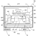
図1は本発明の一実施の形態に係る基板洗浄装置の概略構成を示す模式的平面図であり、図2は図1の基板洗浄装置700を白抜きの矢印Mの方向に見た模式的側面図であり、図3は図1の基板洗浄装置700を白抜きの矢印Nの方向に見た模式的側面図である。
図1〜図3の基板研磨部400および基板洗浄部500は、アーム410,510の他端部に設けられる部材(研磨ヘッドphおよび洗浄ブラシcb)が異なる点を除いて基本的に同じ構成を有する。そこで、基板研磨部400および基板洗浄部500のうち、代表して基板洗浄部500の構成を説明する。
円柱形状を有する洗浄ブラシcbの上端面で基板Wの下面を洗浄する場合、基板Wの下面に付着する汚染物は、主として洗浄ブラシcbの上端面の外周端部で剥ぎ取られる。そのため、洗浄ブラシcbの上端面の外周端部には、基板Wの下面から除去された汚染物が残留しやすい。そこで、ブラシ洗浄部600により洗浄ブラシcbが洗浄される。
まず、図1のスピンチャック200によって保持される基板Wの外周端部の構造を説明する。図7は、基板Wの外周端部の構造を示す拡大側面図である。図7に示すように、基板Wの外周端部WEは、上面側のベベル部1、下面側のベベル部2および端面3を含む。以下の説明においては、基板Wの下面周縁部とは、基板Wのベベル部2から所定の幅だけ内側までの領域を意味し、その幅は研磨ヘッドphおよび洗浄ブラシcbの外径よりも小さい。
図10は図1の基板洗浄装置700の制御系統の構成を示すブロック図である。図10には、研磨洗浄コントローラ780の機能的な構成が示される。研磨洗浄コントローラ780は、スピンチャック制御部781、受け渡し機構制御部782、ガード昇降制御部783、基板研磨制御部784、基板上面用液供給制御部785、ブラシ洗浄用液供給制御部786および基板洗浄制御部790を含む。基板洗浄制御部790は、さらに回転制御部791、昇降制御部792、アーム制御部793および基板下面用液供給制御部794を含む。図10の研磨洗浄コントローラ780の各部の機能は、CPUが制御プログラムを実行することにより実現される。
図1の基板洗浄装置700においては、例えば基板Wが筐体710内に搬入された後、基板Wの上面の洗浄、基板Wの下面の研磨および基板Wの下面の洗浄がこの順で連続的に実行される。このときの基板洗浄装置700の動作について説明する。
図16は、図1の基板洗浄装置700を備えた基板処理装置の模式的平面図である。図16および後述する図17〜図19には、位置関係を明確にするために互いに直交するX方向、Y方向およびZ方向を示す矢印を付している。X方向およびY方向は水平面内で互いに直交し、Z方向は鉛直方向に相当する。
図17は、主として図16の塗布処理部121、塗布現像処理部131および洗浄乾燥処理部161を示す基板処理装置100の模式的側面図である。
図18は、主として図16の熱処理部123,133および洗浄乾燥処理部162を示す基板処理装置100の模式的側面図である。図18に示すように、熱処理部123は、上方に設けられる上段熱処理部301および下方に設けられる下段熱処理部302を有する。上段熱処理部301および下段熱処理部302には、複数の熱処理装置PHP、複数の密着強化処理ユニットPAHPおよび複数の冷却ユニットCPが設けられる。
図19は、主として図16の搬送部122,132,163を示す側面図である。図19に示すように、搬送部122は、上段搬送室125および下段搬送室126を有する。搬送部132は、上段搬送室135および下段搬送室136を有する。上段搬送室125には搬送装置(搬送ロボット)127が設けられ、下段搬送室126には搬送装置128が設けられる。また、上段搬送室135には搬送装置137が設けられ、下段搬送室136には搬送装置138が設けられる。
図16〜図19を参照しながら基板処理装置100の動作を説明する。インデクサブロック11のキャリア載置部111(図16)に、未処理の基板Wが収容されたキャリア113が載置される。搬送装置115は、キャリア113から基板載置部PASS1,PASS3(図19)に未処理の基板Wを搬送する。また、搬送装置115は、基板載置部PASS2,PASS4(図19)に載置された処理済の基板Wをキャリア113に搬送する。
(a)上記の基板洗浄装置700においては、ブラシ洗浄部600により基板洗浄部500の洗浄ブラシcbが洗浄される。洗浄ブラシcbの洗浄時には、空間形成部材620の円形開口624が洗浄ブラシcbの上端面により閉塞された状態で、空間形成部材620の内部空間625に洗浄液が供給される。供給された洗浄液は、円形開口624から洗浄ブラシcbの上端面と空間形成部材620の下端面623との間を通して空間形成部材620の外部に流出する。それにより、洗浄ブラシcbの上端面の外周端部に残留する汚染物が、空間形成部材620の内部空間625から流出する洗浄液とともに洗い流される。その結果、基板Wの下面に付着した汚染物を除去することが可能であるとともに、除去された汚染物の基板Wへの再付着が低減される。
(a)上記実施の形態では、基板洗浄装置700のスピンチャック200に複数の補助ピン290が設けられるが、複数の補助ピン290は設けられなくてもよい。この場合、スピンチャック200の部品点数が低減されるとともにスピンチャック200の構成が単純化する。また、図9のマグネットプレート232Aに対応する領域で各チャックピン220を局部的に開状態とすることにより、研磨ヘッドphが他の部材と干渉しない状態で研磨ヘッドphを基板Wの外周端部WEに接触させることができる。それにより、基板Wの外周端部WE(図7)の研磨が可能になる。さらに、図9のマグネットプレート232Bに対応する領域で各チャックピン220を局部的に開状態とすることにより、洗浄ブラシcbが他の部材と干渉しない状態で洗浄ブラシcbを基板Wの外周端部WEに接触させることができる。それにより、基板Wの外周端部WE(図7)の洗浄が可能になる。
以下、請求項の各構成要素と実施の形態の各構成要素との対応の例について説明するが、本発明は下記の例に限定されない。
3 端面
11 インデクサブロック
12 第1の処理ブロック
13 第2の処理ブロック
14 インターフェイスブロック
14A 洗浄乾燥処理ブロック
14B 搬入搬出ブロック
15 露光装置
15a 基板搬入部
15b 基板搬出部
21,22,23,24,32,34 塗布処理室
25,35,200 スピンチャック
27,37 カップ
28 処理液ノズル
29 ノズル搬送機構
31,33 現像処理室
38 現像ノズル
39 移動機構
50,60 流体ボックス部
81〜84,91〜95 洗浄乾燥処理室
98 流体供給系
99 廃棄系
100 基板処理装置
111 キャリア載置部
112,122,132,163 搬送部
113 キャリア
114 メインコントローラ
115,127,128,137,138,141,142,146 搬送装置
121 塗布処理部
123,133 熱処理部
125,135 上段搬送室
126,136 下段搬送室
129 塗布処理ユニット
131 塗布現像処理部
139 現像処理ユニット
161,162 洗浄乾燥処理部
200 スピンチャック
211 スピンモータ
212,352 回転軸
213 スピンプレート
214 プレート支持部材
215 液供給管
220 チャックピン
221 軸部
222 ピン支持部
223 保持部
224 マグネット
231A,231B,232A,232B マグネットプレート
233A,233B,234A,234B マグネット昇降機構
290 補助ピン
300 ガード機構
301,303 上段熱処理部
302,304 下段熱処理部
310 ガード
320 ガード昇降駆動部
350 受け渡し機構
351 昇降回転駆動部
353,410,510 アーム
354 保持ピン
400 基板研磨部
410N,510N ノズル
420,520 アーム支持柱
500 基板洗浄部
511 アーム一端部
512 アーム本体部
513 アーム他端部
514 回転支持軸
515,517 プーリ
516 ベルト
518 モータ
530 アーム昇降駆動部
531 リニアガイド
532 エアシリンダ
533 電空レギュレータ
540 アーム回転駆動部
541 エンコーダ
600 ブラシ洗浄部
610 支持板
611,621h 貫通孔
620 空間形成部材
621 円板部
622 円筒部
623 下端面
624 円形開口
625 内部空間
630 洗浄液導入管
700 基板洗浄装置
710 筐体
711〜714 側壁
715 天井部
716 底面部
720 液受けバット
721 廃液部
780 研磨洗浄コントローラ
781 スピンチャック制御部
782 受け渡し機構制御部
783 ガード昇降制御部
784 基板研磨制御部
785 基板上面用液供給制御部
786 ブラシ洗浄用液供給制御部
790 基板洗浄制御部
791 回転制御部
792 昇降制御部
793 アーム制御部
794 基板下面用液供給制御部
cb 洗浄ブラシ
CP 冷却ユニット
EEW エッジ露光部
P−BF1,P−BF2 載置兼バッファ部
P−CP 載置兼冷却部
p1 ヘッド待機位置
p2 ブラシ待機位置
PAHP 密着強化処理ユニット
PASS1〜PASS9 基板載置部
ph 研磨ヘッド
PHP 熱処理装置
SD2 洗浄乾燥処理ユニット
W 基板
WE 外周端部
Claims (7)
- 基板の下面を洗浄する基板洗浄装置であって、
基板を水平姿勢で保持して回転させる回転保持部と、
円形の上端面を有する洗浄具を含み、前記回転保持部により回転される基板の下面に前記洗浄具の前記上端面を接触させることにより基板の下面を洗浄する下面洗浄部と、
前記洗浄具を洗浄する洗浄具洗浄部とを備え、
前記洗浄具洗浄部は、
下端面を有しかつ前記下端面に円形開口を有する内部空間を形成する空間形成部材と、
前記空間形成部材の前記円形開口が前記洗浄具の前記上端面により閉塞された状態で前記空間形成部材の前記内部空間に洗浄液を供給することにより、前記内部空間から前記円形開口および前記洗浄具の前記上端面と前記空間形成部材の前記下端面との間を通して洗浄液を流出させる洗浄液供給系とを含む、基板洗浄装置。 - 前記空間形成部材の前記下端面は、前記円形開口の内縁から斜め下方かつ外方に向かって傾斜する、請求項1記載の基板洗浄装置。
- 前記空間形成部材の前記円形開口が前記洗浄具の前記上端面により閉塞された状態で、前記上端面を通る鉛直軸の周りで前記洗浄具を前記空間形成部材に対して相対的に回転させる洗浄具回転部をさらに備える、請求項1または2記載の基板洗浄装置。
- 前記洗浄具の前記上端面が前記空間形成部材の前記円形開口を閉塞するように前記洗浄具を前記空間形成部材に対して相対的に移動させる相対的移動部をさらに備える、請求項1〜3のいずれか一項に記載の基板洗浄装置。
- 前記洗浄具洗浄部は、前記回転保持部により回転される基板の外方の待機位置に設けられ、
前記相対的移動部は、基板の下面の洗浄時に、前記洗浄具を前記洗浄具の前記上端面が前記回転保持部により回転される基板の下面に対向する洗浄位置と前記待機位置との間で移動させるとともに、前記洗浄位置で前記洗浄具の前記上端面が前記回転保持部により回転される基板の下面に接触するように、前記洗浄具を前記回転保持部により回転される基板に対して相対的に移動させることが可能に構成された、請求項4記載の基板洗浄装置。 - 研磨具を含み、前記回転保持部により回転される基板の下面に前記研磨具を接触させることにより基板の下面を研磨する下面研磨部をさらに備え、
前記下面洗浄部は、前記下面研磨部による基板の下面の研磨後に当該基板の下面を洗浄する、請求項1〜5のいずれか一項に記載の基板洗浄装置。 - 露光装置に隣接するように配置される基板処理装置であって、
基板の上面に感光性膜を塗布する塗布装置と、
請求項1〜6のいずれか一項に記載の基板洗浄装置と、
前記塗布装置、前記基板洗浄装置および前記露光装置の間で基板を搬送する搬送装置とを備え、
前記基板洗浄装置は、前記露光装置による基板の露光処理前に基板の下面を洗浄する、基板処理装置。
Priority Applications (5)
| Application Number | Priority Date | Filing Date | Title |
|---|---|---|---|
| JP2016172672A JP6684191B2 (ja) | 2016-09-05 | 2016-09-05 | 基板洗浄装置およびそれを備える基板処理装置 |
| TW106128549A TWI674153B (zh) | 2016-09-05 | 2017-08-23 | 基板洗淨裝置及具備其之基板處理裝置 |
| US15/691,929 US10331049B2 (en) | 2016-09-05 | 2017-08-31 | Substrate cleaning device and substrate processing apparatus including the same |
| CN201710779419.5A CN107799442B (zh) | 2016-09-05 | 2017-09-01 | 基板清洗装置及具备该基板清洗装置的基板处理装置 |
| KR1020170111729A KR101972226B1 (ko) | 2016-09-05 | 2017-09-01 | 기판 세정 장치 및 그것을 구비하는 기판 처리 장치 |
Applications Claiming Priority (1)
| Application Number | Priority Date | Filing Date | Title |
|---|---|---|---|
| JP2016172672A JP6684191B2 (ja) | 2016-09-05 | 2016-09-05 | 基板洗浄装置およびそれを備える基板処理装置 |
Publications (3)
| Publication Number | Publication Date |
|---|---|
| JP2018041754A JP2018041754A (ja) | 2018-03-15 |
| JP2018041754A5 JP2018041754A5 (ja) | 2019-09-12 |
| JP6684191B2 true JP6684191B2 (ja) | 2020-04-22 |
Family
ID=61282178
Family Applications (1)
| Application Number | Title | Priority Date | Filing Date |
|---|---|---|---|
| JP2016172672A Active JP6684191B2 (ja) | 2016-09-05 | 2016-09-05 | 基板洗浄装置およびそれを備える基板処理装置 |
Country Status (5)
| Country | Link |
|---|---|
| US (1) | US10331049B2 (ja) |
| JP (1) | JP6684191B2 (ja) |
| KR (1) | KR101972226B1 (ja) |
| CN (1) | CN107799442B (ja) |
| TW (1) | TWI674153B (ja) |
Families Citing this family (3)
| Publication number | Priority date | Publication date | Assignee | Title |
|---|---|---|---|---|
| KR102081706B1 (ko) * | 2018-07-18 | 2020-02-27 | 세메스 주식회사 | 기판 처리 방법 및 기판 처리 장치 |
| CN111069115A (zh) * | 2018-10-22 | 2020-04-28 | 长鑫存储技术有限公司 | 一种cmp后清洗方法 |
| CN111341699B (zh) * | 2020-03-09 | 2023-03-31 | 杭州众硅电子科技有限公司 | 一种清洗刷预清洗系统 |
Family Cites Families (39)
| Publication number | Priority date | Publication date | Assignee | Title |
|---|---|---|---|---|
| TW316995B (ja) * | 1995-01-19 | 1997-10-01 | Tokyo Electron Co Ltd | |
| TW434052B (en) * | 1996-02-20 | 2001-05-16 | Pre Tech Co Ltd | Washing device of disk to be washed |
| JP3756284B2 (ja) | 1997-04-30 | 2006-03-15 | 大日本スクリーン製造株式会社 | 基板洗浄装置 |
| US6115867A (en) * | 1997-08-18 | 2000-09-12 | Tokyo Electron Limited | Apparatus for cleaning both sides of substrate |
| JP3415435B2 (ja) * | 1998-04-03 | 2003-06-09 | 東京エレクトロン株式会社 | 処理装置及び処理方法 |
| JP4334758B2 (ja) * | 1999-12-17 | 2009-09-30 | 東京エレクトロン株式会社 | 膜形成装置 |
| US6418584B1 (en) * | 2000-05-24 | 2002-07-16 | Speedfam-Ipec Corporation | Apparatus and process for cleaning a work piece |
| JP3888608B2 (ja) * | 2001-04-25 | 2007-03-07 | 東京エレクトロン株式会社 | 基板両面処理装置 |
| JP2003007664A (ja) * | 2001-06-22 | 2003-01-10 | Ses Co Ltd | 枚葉式基板洗浄方法および枚葉式基板洗浄装置 |
| JP2003243350A (ja) * | 2002-02-14 | 2003-08-29 | Tokyo Electron Ltd | スクラブ洗浄装置におけるブラシクリーニング方法及び処理システム |
| JP2006278392A (ja) * | 2005-03-28 | 2006-10-12 | Dainippon Screen Mfg Co Ltd | 基板洗浄装置および基板洗浄方法 |
| KR100795622B1 (ko) * | 2005-03-30 | 2008-01-17 | 다이닛뽕스크린 세이조오 가부시키가이샤 | 기판처리장치 및 기판처리방법 |
| JP4726752B2 (ja) * | 2005-10-25 | 2011-07-20 | 義治 山本 | 基板洗浄装置 |
| KR100892809B1 (ko) * | 2006-03-30 | 2009-04-10 | 다이닛뽕스크린 세이조오 가부시키가이샤 | 기판처리장치 및 기판처리방법 |
| US20070251035A1 (en) * | 2006-05-01 | 2007-11-01 | Taiwan Semiconductor Manufacturing Co., Ltd. | Cleaning device |
| JP4796542B2 (ja) * | 2007-05-30 | 2011-10-19 | 株式会社プレテック | 洗浄装置 |
| JP4939376B2 (ja) | 2007-11-13 | 2012-05-23 | 株式会社Sokudo | 基板処理装置 |
| JP5091687B2 (ja) * | 2008-01-08 | 2012-12-05 | 株式会社Sokudo | 基板処理装置 |
| KR101423611B1 (ko) * | 2008-01-16 | 2014-07-30 | 삼성전자주식회사 | 기판 처리 장치, 노광 장치 및 클리닝 툴의 세정 방법 |
| JP2010287686A (ja) * | 2009-06-10 | 2010-12-24 | Tokyo Electron Ltd | 塗布、現像装置及び基板の裏面洗浄方法。 |
| JP5437168B2 (ja) * | 2009-08-07 | 2014-03-12 | 東京エレクトロン株式会社 | 基板の液処理装置および液処理方法 |
| US20120285484A1 (en) * | 2011-05-13 | 2012-11-15 | Li-Chung Liu | Method for cleaning a semiconductor wafer |
| TWI524456B (zh) * | 2011-11-04 | 2016-03-01 | 東京威力科創股份有限公司 | 基板處理系統、基板運送方法、程式及電腦記憶媒體 |
| TWI550686B (zh) * | 2011-11-04 | 2016-09-21 | 東京威力科創股份有限公司 | 基板處理系統、基板運送方法及電腦記憶媒體 |
| JP5637974B2 (ja) * | 2011-11-28 | 2014-12-10 | 東京エレクトロン株式会社 | 基板洗浄装置及び基板洗浄方法 |
| US9119464B2 (en) * | 2012-01-31 | 2015-09-01 | Taiwan Semiconductor Manufacturing Company, Ltd. | Brush cleaning system |
| JP6001896B2 (ja) * | 2012-03-27 | 2016-10-05 | 株式会社Screenセミコンダクターソリューションズ | 基板洗浄装置およびそれを備えた基板処理装置 |
| JP6061484B2 (ja) * | 2012-03-27 | 2017-01-18 | 株式会社Screenセミコンダクターソリューションズ | 基板洗浄装置およびそれを備えた基板処理装置 |
| JP5887227B2 (ja) * | 2012-08-07 | 2016-03-16 | 株式会社荏原製作所 | ドレッサーディスク洗浄用ブラシ、洗浄装置及び洗浄方法 |
| US9211568B2 (en) | 2013-03-12 | 2015-12-15 | Taiwan Semiconductor Manufacturing Company Limited | Clean function for semiconductor wafer scrubber |
| JP6143589B2 (ja) | 2013-07-12 | 2017-06-07 | 株式会社Screenホールディングス | 基板処理装置 |
| JP6066861B2 (ja) * | 2013-08-05 | 2017-01-25 | 東京エレクトロン株式会社 | 基板洗浄装置、基板の裏面洗浄方法及び洗浄機構 |
| KR20150075357A (ko) * | 2013-12-25 | 2015-07-03 | 가부시키가이샤 에바라 세이사꾸쇼 | 기판 세정 장치 및 기판 처리 장치 |
| SG10201906815XA (en) * | 2014-08-26 | 2019-08-27 | Ebara Corp | Substrate processing apparatus |
| CN106714987B (zh) * | 2014-09-26 | 2019-04-02 | 盛美半导体设备(上海)有限公司 | 清洗半导体硅片的装置和方法 |
| JP6503194B2 (ja) * | 2015-02-16 | 2019-04-17 | 株式会社Screenホールディングス | 基板処理装置 |
| JP6751634B2 (ja) * | 2016-09-21 | 2020-09-09 | 株式会社Screenホールディングス | 基板処理装置 |
| TWI821887B (zh) * | 2016-11-29 | 2023-11-11 | 日商東京威力科創股份有限公司 | 基板處理裝置、基板處理方法及記錄媒體 |
| JP6885754B2 (ja) * | 2017-03-09 | 2021-06-16 | 株式会社Screenホールディングス | 基板処理方法および基板処理装置 |
-
2016
- 2016-09-05 JP JP2016172672A patent/JP6684191B2/ja active Active
-
2017
- 2017-08-23 TW TW106128549A patent/TWI674153B/zh active
- 2017-08-31 US US15/691,929 patent/US10331049B2/en active Active
- 2017-09-01 KR KR1020170111729A patent/KR101972226B1/ko active IP Right Grant
- 2017-09-01 CN CN201710779419.5A patent/CN107799442B/zh active Active
Also Published As
| Publication number | Publication date |
|---|---|
| US20180067407A1 (en) | 2018-03-08 |
| US10331049B2 (en) | 2019-06-25 |
| KR101972226B1 (ko) | 2019-04-24 |
| TWI674153B (zh) | 2019-10-11 |
| CN107799442B (zh) | 2021-09-14 |
| TW201811453A (zh) | 2018-04-01 |
| CN107799442A (zh) | 2018-03-13 |
| KR20180027357A (ko) | 2018-03-14 |
| JP2018041754A (ja) | 2018-03-15 |
Similar Documents
| Publication | Publication Date | Title |
|---|---|---|
| JP6740065B2 (ja) | 基板洗浄装置、基板処理装置、基板洗浄方法および基板処理方法 | |
| KR101798320B1 (ko) | 기판 처리 장치 | |
| JP6740066B2 (ja) | 基板洗浄装置、基板処理装置および基板洗浄方法 | |
| JP4757882B2 (ja) | 基板洗浄装置、基板洗浄方法、基板処理システムならびに記録媒体 | |
| JP2021073706A (ja) | 基板処理装置 | |
| JP2006012880A (ja) | 基板反転装置、基板搬送装置、基板処理装置、基板反転方法、基板搬送方法および基板処理方法 | |
| JP6992131B2 (ja) | 基板洗浄装置、基板処理装置、基板洗浄方法および基板処理方法 | |
| JP6684191B2 (ja) | 基板洗浄装置およびそれを備える基板処理装置 | |
| JP2019046892A (ja) | 基板処理方法および基板処理装置 | |
| JP2010093265A (ja) | 処理液供給ユニットとこれを利用した基板処理装置及び方法 | |
| JP3958572B2 (ja) | 基板処理装置及び基板処理方法 | |
| JP7445698B2 (ja) | 基板処理装置及び方法 | |
| US20240100572A1 (en) | Apparatus for treating substrate and method for treating a substrate | |
| US11940734B2 (en) | Apparatus and method for treating substrate | |
| CN116994981A (zh) | 用于处理基板的设备和方法 | |
| KR20230024704A (ko) | 기판 처리 장치 및 기판 처리 방법 |
Legal Events
| Date | Code | Title | Description |
|---|---|---|---|
| A621 | Written request for application examination |
Free format text: JAPANESE INTERMEDIATE CODE: A621 Effective date: 20190624 |
|
| A521 | Request for written amendment filed |
Free format text: JAPANESE INTERMEDIATE CODE: A523 Effective date: 20190802 |
|
| A977 | Report on retrieval |
Free format text: JAPANESE INTERMEDIATE CODE: A971007 Effective date: 20200313 |
|
| TRDD | Decision of grant or rejection written | ||
| A01 | Written decision to grant a patent or to grant a registration (utility model) |
Free format text: JAPANESE INTERMEDIATE CODE: A01 Effective date: 20200317 |
|
| A61 | First payment of annual fees (during grant procedure) |
Free format text: JAPANESE INTERMEDIATE CODE: A61 Effective date: 20200327 |
|
| R150 | Certificate of patent or registration of utility model |
Ref document number: 6684191 Country of ref document: JP Free format text: JAPANESE INTERMEDIATE CODE: R150 |
|
| R250 | Receipt of annual fees |
Free format text: JAPANESE INTERMEDIATE CODE: R250 |
|
| R250 | Receipt of annual fees |
Free format text: JAPANESE INTERMEDIATE CODE: R250 |