JP6412721B2 - 液晶表示装置 - Google Patents
液晶表示装置 Download PDFInfo
- Publication number
- JP6412721B2 JP6412721B2 JP2014120613A JP2014120613A JP6412721B2 JP 6412721 B2 JP6412721 B2 JP 6412721B2 JP 2014120613 A JP2014120613 A JP 2014120613A JP 2014120613 A JP2014120613 A JP 2014120613A JP 6412721 B2 JP6412721 B2 JP 6412721B2
- Authority
- JP
- Japan
- Prior art keywords
- liquid crystal
- crystal display
- light shielding
- shielding tape
- display panel
- Prior art date
- Legal status (The legal status is an assumption and is not a legal conclusion. Google has not performed a legal analysis and makes no representation as to the accuracy of the status listed.)
- Active
Links
Images


Classifications
-
- G—PHYSICS
- G02—OPTICS
- G02F—OPTICAL DEVICES OR ARRANGEMENTS FOR THE CONTROL OF LIGHT BY MODIFICATION OF THE OPTICAL PROPERTIES OF THE MEDIA OF THE ELEMENTS INVOLVED THEREIN; NON-LINEAR OPTICS; FREQUENCY-CHANGING OF LIGHT; OPTICAL LOGIC ELEMENTS; OPTICAL ANALOGUE/DIGITAL CONVERTERS
- G02F1/00—Devices or arrangements for the control of the intensity, colour, phase, polarisation or direction of light arriving from an independent light source, e.g. switching, gating or modulating; Non-linear optics
- G02F1/01—Devices or arrangements for the control of the intensity, colour, phase, polarisation or direction of light arriving from an independent light source, e.g. switching, gating or modulating; Non-linear optics for the control of the intensity, phase, polarisation or colour
- G02F1/13—Devices or arrangements for the control of the intensity, colour, phase, polarisation or direction of light arriving from an independent light source, e.g. switching, gating or modulating; Non-linear optics for the control of the intensity, phase, polarisation or colour based on liquid crystals, e.g. single liquid crystal display cells
- G02F1/133—Constructional arrangements; Operation of liquid crystal cells; Circuit arrangements
- G02F1/1333—Constructional arrangements; Manufacturing methods
- G02F1/13338—Input devices, e.g. touch panels
-
- G—PHYSICS
- G02—OPTICS
- G02F—OPTICAL DEVICES OR ARRANGEMENTS FOR THE CONTROL OF LIGHT BY MODIFICATION OF THE OPTICAL PROPERTIES OF THE MEDIA OF THE ELEMENTS INVOLVED THEREIN; NON-LINEAR OPTICS; FREQUENCY-CHANGING OF LIGHT; OPTICAL LOGIC ELEMENTS; OPTICAL ANALOGUE/DIGITAL CONVERTERS
- G02F1/00—Devices or arrangements for the control of the intensity, colour, phase, polarisation or direction of light arriving from an independent light source, e.g. switching, gating or modulating; Non-linear optics
- G02F1/01—Devices or arrangements for the control of the intensity, colour, phase, polarisation or direction of light arriving from an independent light source, e.g. switching, gating or modulating; Non-linear optics for the control of the intensity, phase, polarisation or colour
- G02F1/13—Devices or arrangements for the control of the intensity, colour, phase, polarisation or direction of light arriving from an independent light source, e.g. switching, gating or modulating; Non-linear optics for the control of the intensity, phase, polarisation or colour based on liquid crystals, e.g. single liquid crystal display cells
- G02F1/133—Constructional arrangements; Operation of liquid crystal cells; Circuit arrangements
- G02F1/1333—Constructional arrangements; Manufacturing methods
- G02F1/1335—Structural association of cells with optical devices, e.g. polarisers or reflectors
- G02F1/133509—Filters, e.g. light shielding masks
- G02F1/133512—Light shielding layers, e.g. black matrix
-
- G—PHYSICS
- G02—OPTICS
- G02F—OPTICAL DEVICES OR ARRANGEMENTS FOR THE CONTROL OF LIGHT BY MODIFICATION OF THE OPTICAL PROPERTIES OF THE MEDIA OF THE ELEMENTS INVOLVED THEREIN; NON-LINEAR OPTICS; FREQUENCY-CHANGING OF LIGHT; OPTICAL LOGIC ELEMENTS; OPTICAL ANALOGUE/DIGITAL CONVERTERS
- G02F1/00—Devices or arrangements for the control of the intensity, colour, phase, polarisation or direction of light arriving from an independent light source, e.g. switching, gating or modulating; Non-linear optics
- G02F1/01—Devices or arrangements for the control of the intensity, colour, phase, polarisation or direction of light arriving from an independent light source, e.g. switching, gating or modulating; Non-linear optics for the control of the intensity, phase, polarisation or colour
- G02F1/13—Devices or arrangements for the control of the intensity, colour, phase, polarisation or direction of light arriving from an independent light source, e.g. switching, gating or modulating; Non-linear optics for the control of the intensity, phase, polarisation or colour based on liquid crystals, e.g. single liquid crystal display cells
- G02F1/133—Constructional arrangements; Operation of liquid crystal cells; Circuit arrangements
- G02F1/1333—Constructional arrangements; Manufacturing methods
- G02F1/133308—Support structures for LCD panels, e.g. frames or bezels
-
- G—PHYSICS
- G02—OPTICS
- G02F—OPTICAL DEVICES OR ARRANGEMENTS FOR THE CONTROL OF LIGHT BY MODIFICATION OF THE OPTICAL PROPERTIES OF THE MEDIA OF THE ELEMENTS INVOLVED THEREIN; NON-LINEAR OPTICS; FREQUENCY-CHANGING OF LIGHT; OPTICAL LOGIC ELEMENTS; OPTICAL ANALOGUE/DIGITAL CONVERTERS
- G02F1/00—Devices or arrangements for the control of the intensity, colour, phase, polarisation or direction of light arriving from an independent light source, e.g. switching, gating or modulating; Non-linear optics
- G02F1/01—Devices or arrangements for the control of the intensity, colour, phase, polarisation or direction of light arriving from an independent light source, e.g. switching, gating or modulating; Non-linear optics for the control of the intensity, phase, polarisation or colour
- G02F1/13—Devices or arrangements for the control of the intensity, colour, phase, polarisation or direction of light arriving from an independent light source, e.g. switching, gating or modulating; Non-linear optics for the control of the intensity, phase, polarisation or colour based on liquid crystals, e.g. single liquid crystal display cells
- G02F1/133—Constructional arrangements; Operation of liquid crystal cells; Circuit arrangements
- G02F1/1333—Constructional arrangements; Manufacturing methods
- G02F1/1335—Structural association of cells with optical devices, e.g. polarisers or reflectors
- G02F1/1336—Illuminating devices
-
- G—PHYSICS
- G02—OPTICS
- G02F—OPTICAL DEVICES OR ARRANGEMENTS FOR THE CONTROL OF LIGHT BY MODIFICATION OF THE OPTICAL PROPERTIES OF THE MEDIA OF THE ELEMENTS INVOLVED THEREIN; NON-LINEAR OPTICS; FREQUENCY-CHANGING OF LIGHT; OPTICAL LOGIC ELEMENTS; OPTICAL ANALOGUE/DIGITAL CONVERTERS
- G02F1/00—Devices or arrangements for the control of the intensity, colour, phase, polarisation or direction of light arriving from an independent light source, e.g. switching, gating or modulating; Non-linear optics
- G02F1/01—Devices or arrangements for the control of the intensity, colour, phase, polarisation or direction of light arriving from an independent light source, e.g. switching, gating or modulating; Non-linear optics for the control of the intensity, phase, polarisation or colour
- G02F1/13—Devices or arrangements for the control of the intensity, colour, phase, polarisation or direction of light arriving from an independent light source, e.g. switching, gating or modulating; Non-linear optics for the control of the intensity, phase, polarisation or colour based on liquid crystals, e.g. single liquid crystal display cells
- G02F1/133—Constructional arrangements; Operation of liquid crystal cells; Circuit arrangements
- G02F1/1333—Constructional arrangements; Manufacturing methods
- G02F1/1339—Gaskets; Spacers; Sealing of cells
-
- G—PHYSICS
- G02—OPTICS
- G02F—OPTICAL DEVICES OR ARRANGEMENTS FOR THE CONTROL OF LIGHT BY MODIFICATION OF THE OPTICAL PROPERTIES OF THE MEDIA OF THE ELEMENTS INVOLVED THEREIN; NON-LINEAR OPTICS; FREQUENCY-CHANGING OF LIGHT; OPTICAL LOGIC ELEMENTS; OPTICAL ANALOGUE/DIGITAL CONVERTERS
- G02F1/00—Devices or arrangements for the control of the intensity, colour, phase, polarisation or direction of light arriving from an independent light source, e.g. switching, gating or modulating; Non-linear optics
- G02F1/01—Devices or arrangements for the control of the intensity, colour, phase, polarisation or direction of light arriving from an independent light source, e.g. switching, gating or modulating; Non-linear optics for the control of the intensity, phase, polarisation or colour
- G02F1/13—Devices or arrangements for the control of the intensity, colour, phase, polarisation or direction of light arriving from an independent light source, e.g. switching, gating or modulating; Non-linear optics for the control of the intensity, phase, polarisation or colour based on liquid crystals, e.g. single liquid crystal display cells
- G02F1/133—Constructional arrangements; Operation of liquid crystal cells; Circuit arrangements
- G02F1/1333—Constructional arrangements; Manufacturing methods
- G02F1/133308—Support structures for LCD panels, e.g. frames or bezels
- G02F1/133314—Back frames
-
- G—PHYSICS
- G02—OPTICS
- G02F—OPTICAL DEVICES OR ARRANGEMENTS FOR THE CONTROL OF LIGHT BY MODIFICATION OF THE OPTICAL PROPERTIES OF THE MEDIA OF THE ELEMENTS INVOLVED THEREIN; NON-LINEAR OPTICS; FREQUENCY-CHANGING OF LIGHT; OPTICAL LOGIC ELEMENTS; OPTICAL ANALOGUE/DIGITAL CONVERTERS
- G02F2201/00—Constructional arrangements not provided for in groups G02F1/00 - G02F7/00
- G02F2201/50—Protective arrangements
Description
(4)前記遮光テープの他方の側の前記粘着材は、前記遮光テープの周方向に所定の長さ、存在していない部分があることを特徴とする(1)に記載の液晶表示装置。
Claims (7)
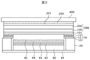
- バックライトを収容するモールドの上に液晶表示パネルが遮光テープによって接着し、前記液晶表示パネルの上にタッチパネルが接着している液晶表示装置であって、
前記液晶表示パネルは表示領域を有し、
前記遮光テープは、黒色の基材の両側に粘着材が形成された構成であり、
前記遮光テープの、前記液晶表示パネルの辺に沿って延在する方向を周方向と定義し、前記周方向と直角方向を幅と定義したとき、
前記遮光テープは、前記表示領域の周囲を取り囲むように途切れることなく形成され、
前記遮光テープの一方の側の前記粘着材は、前記遮光テープの周方向に所定の長さ、前記遮光テープの前記幅全体に渡って、存在していない部分があることを特徴とする液晶表示装置。 - 前記タッチパネルは前記液晶表示パネルに紫外線硬化樹脂によって接着していることを特徴とする請求項1に記載の液晶表示装置。
- 前記遮光テープの前記粘着材が存在していない部分の前記遮光テープの周方向の前記所定の長さは2mm以下であることを特徴とする請求項1に記載の液晶表示装置。
- 前記遮光テープの他方の側の前記粘着材は、前記遮光テープの周方向に所定の長さ、存在していない部分があることを特徴とする請求項1に記載の液晶表示装置。
- 前記タッチパネルの上にさらにフロントウインドウが形成されていることを特徴とする請求項1乃至4のいずれか1項に記載の液晶表示装置。
- バックライトを収容するモールドの上に液晶表示パネルが遮光テープによって接着し、前記液晶表示パネルの上にタッチパネルが接着している液晶表示装置であって、
前記液晶表示パネルは表示領域を有し、
前記遮光テープは、黒色の基材の両側に粘着材が形成された構成であり、
前記遮光テープの、前記液晶表示パネルの辺に沿って延在する方向を周方向と定義し、前記周方向と直角方向を幅と定義したとき、
前記遮光テープは、前記表示領域の周囲を取り囲むように途切れることなく形成され、
前記遮光テープの一方の側の前記粘着材は、前記遮光テープの周方向に所定の長さ、前記遮光テープの前記幅全体に渡って、非粘着性の物質がコーティングされていることを特徴とする液晶表示装置。 - バックライトを収容するモールドの上に液晶表示パネルが遮光テープによって接着し、前記液晶表示パネルの上にフロントウインドウが接着している液晶表示装置であって、
前記液晶表示パネルは表示領域を有し、
前記遮光テープは、黒色の基材の両側に粘着材が形成された構成であり、
前記遮光テープの、前記液晶表示パネルの辺に沿って延在する方向を周方向と定義し、前記周方向と直角方向を幅と定義したとき、
前記遮光テープは、前記表示領域の周囲を取り囲むように途切れることなく形成され、
前記遮光テープの一方の側の前記粘着材は、前記遮光テープの周方向に所定の長さ、前記遮光テープの前記幅全体に渡って、存在していない部分があることを特徴とする液晶表示装置。
Priority Applications (3)
| Application Number | Priority Date | Filing Date | Title |
|---|---|---|---|
| JP2014120613A JP6412721B2 (ja) | 2014-06-11 | 2014-06-11 | 液晶表示装置 |
| CN201510309789.3A CN105278138B (zh) | 2014-06-11 | 2015-06-08 | 液晶显示装置 |
| US14/734,770 US9581851B2 (en) | 2014-06-11 | 2015-06-09 | Liquid crystal display device |
Applications Claiming Priority (1)
| Application Number | Priority Date | Filing Date | Title |
|---|---|---|---|
| JP2014120613A JP6412721B2 (ja) | 2014-06-11 | 2014-06-11 | 液晶表示装置 |
Publications (3)
| Publication Number | Publication Date |
|---|---|
| JP2016001232A JP2016001232A (ja) | 2016-01-07 |
| JP2016001232A5 JP2016001232A5 (ja) | 2017-07-13 |
| JP6412721B2 true JP6412721B2 (ja) | 2018-10-24 |
Family
ID=54836042
Family Applications (1)
| Application Number | Title | Priority Date | Filing Date |
|---|---|---|---|
| JP2014120613A Active JP6412721B2 (ja) | 2014-06-11 | 2014-06-11 | 液晶表示装置 |
Country Status (3)
| Country | Link |
|---|---|
| US (1) | US9581851B2 (ja) |
| JP (1) | JP6412721B2 (ja) |
| CN (1) | CN105278138B (ja) |
Families Citing this family (11)
| Publication number | Priority date | Publication date | Assignee | Title |
|---|---|---|---|---|
| KR101920014B1 (ko) * | 2015-10-26 | 2018-11-19 | 주식회사 모다이노칩 | 압력 센서 및 이를 구비하는 터치 입력 장치 |
| CN105974635A (zh) * | 2016-07-18 | 2016-09-28 | 京东方科技集团股份有限公司 | 遮光胶带、应用该遮光胶带的显示装置及其制备方法 |
| CN105974669B (zh) * | 2016-07-22 | 2019-04-05 | 京东方科技集团股份有限公司 | 一种背光模组、显示装置及其控制方法 |
| WO2018180836A1 (ja) * | 2017-03-29 | 2018-10-04 | シャープ株式会社 | 表示装置および表示装置の製造方法 |
| CN107526198B (zh) * | 2017-08-23 | 2020-07-28 | 京东方科技集团股份有限公司 | 一种显示装置 |
| WO2019106334A1 (en) * | 2017-11-28 | 2019-06-06 | P2I Ltd | Electrical or electronic device with a screen having an air vent |
| CN110609412A (zh) * | 2018-06-15 | 2019-12-24 | 夏普株式会社 | 照明装置、显示装置 |
| JP2021071526A (ja) * | 2019-10-29 | 2021-05-06 | 凸版印刷株式会社 | 液晶表示装置 |
| WO2021200364A1 (ja) * | 2020-03-30 | 2021-10-07 | 住友化学株式会社 | 積層体 |
| CN115335740A (zh) * | 2020-03-30 | 2022-11-11 | 住友化学株式会社 | 层叠体 |
| JP2023039702A (ja) * | 2021-09-09 | 2023-03-22 | 株式会社ジャパンディスプレイ | 表示装置 |
Family Cites Families (15)
| Publication number | Priority date | Publication date | Assignee | Title |
|---|---|---|---|---|
| US8060168B2 (en) * | 2007-08-20 | 2011-11-15 | Sony Ericsson Mobile Communications Ab | Dust sealing tape and display using same and method of sealing |
| JP5134327B2 (ja) | 2007-09-26 | 2013-01-30 | 株式会社ジャパンディスプレイイースト | 表示装置 |
| JP4575486B2 (ja) * | 2007-10-24 | 2010-11-04 | セイコーインスツル株式会社 | 表示装置 |
| JP5147610B2 (ja) * | 2008-09-05 | 2013-02-20 | 株式会社ジャパンディスプレイイースト | 液晶表示装置 |
| JP5308749B2 (ja) * | 2008-09-05 | 2013-10-09 | 株式会社ジャパンディスプレイ | 液晶表示装置 |
| US8068197B2 (en) * | 2009-01-19 | 2011-11-29 | Hitachi Displays, Ltd. | Liquid crystal display device |
| JP5287415B2 (ja) * | 2009-03-27 | 2013-09-11 | カシオ計算機株式会社 | バックライト付き液晶モジュール |
| CN201576147U (zh) * | 2009-08-10 | 2010-09-08 | 浙江新力光电科技有限公司 | 液晶显示模组遮光胶带结构 |
| KR20110019823A (ko) * | 2009-08-21 | 2011-03-02 | 주식회사 토비스 | 디스플레이 모듈 및 그를 구비한 단말기 |
| WO2011162019A1 (ja) * | 2010-06-22 | 2011-12-29 | シャープ株式会社 | 表示パネルおよび表示装置 |
| JP2012242765A (ja) * | 2011-05-24 | 2012-12-10 | Japan Display East Co Ltd | 液晶表示装置 |
| WO2013061897A1 (ja) * | 2011-10-28 | 2013-05-02 | シャープ株式会社 | バックライト装置、及び、それを備えた表示装置 |
| TW201341894A (zh) * | 2012-04-06 | 2013-10-16 | Au Optronics Corp | 顯示裝置及其組裝方法 |
| CN104063084B (zh) * | 2013-03-22 | 2017-11-17 | 群创光电股份有限公司 | 触控显示装置 |
| CN103672724B (zh) * | 2013-11-27 | 2016-08-17 | 京东方科技集团股份有限公司 | 一种背光模组遮光结构、背光模组及显示装置 |
-
2014
- 2014-06-11 JP JP2014120613A patent/JP6412721B2/ja active Active
-
2015
- 2015-06-08 CN CN201510309789.3A patent/CN105278138B/zh active Active
- 2015-06-09 US US14/734,770 patent/US9581851B2/en active Active
Also Published As
| Publication number | Publication date |
|---|---|
| US9581851B2 (en) | 2017-02-28 |
| JP2016001232A (ja) | 2016-01-07 |
| CN105278138A (zh) | 2016-01-27 |
| US20150362775A1 (en) | 2015-12-17 |
| CN105278138B (zh) | 2019-06-25 |
Similar Documents
| Publication | Publication Date | Title |
|---|---|---|
| JP6412721B2 (ja) | 液晶表示装置 | |
| JP5297668B2 (ja) | 液晶表示装置 | |
| JP5451036B2 (ja) | 表示装置及びその製造方法 | |
| JP5134327B2 (ja) | 表示装置 | |
| JP4679985B2 (ja) | 液晶表示装置 | |
| CN106019666B (zh) | 显示装置及显示装置的制造方法 | |
| JP2018004728A (ja) | 表示装置および接着方法 | |
| WO2016176929A1 (zh) | 背光模块及液晶显示器 | |
| JP2010256682A (ja) | 液晶表示装置 | |
| JP2016161871A (ja) | 表示装置 | |
| US8964150B2 (en) | Liquid crystal display device and method of manufacturing the same | |
| US9933557B2 (en) | Backlight modules and liquid crystal devices (LCDS) | |
| US9664938B2 (en) | Display device | |
| JP2010134004A (ja) | 表示装置 | |
| WO2016101372A1 (zh) | 液晶面板与背光模组定位胶结构及显示器 | |
| TW201310145A (zh) | 顯示裝置及其顯示面板的固定方法 | |
| US20170357123A1 (en) | Liquid crystal display module and method for fabricating the same, display device | |
| CN109752874B (zh) | 面板模块及显示装置 | |
| US20160274687A1 (en) | Explosion-proof membrane assembly, touch screen structure and display device | |
| TW202026722A (zh) | 顯示裝置 | |
| WO2013118475A1 (ja) | 表示装置 | |
| WO2017024756A1 (zh) | 灯条、背光模组及其组装方法、显示装置 | |
| JP2017120310A (ja) | 表示装置、表示装置に用いる接着シート、および表示装置の製造方法 | |
| JP2009265237A (ja) | 液晶表示装置 | |
| US8675155B2 (en) | Liquid crystal display device comprising a first polarizing plate with a cut portion formed directly below a driving chip wherein the cut portion is covered by a bottom surface of a first substrate |
Legal Events
| Date | Code | Title | Description |
|---|---|---|---|
| A521 | Request for written amendment filed |
Free format text: JAPANESE INTERMEDIATE CODE: A523 Effective date: 20170605 |
|
| A621 | Written request for application examination |
Free format text: JAPANESE INTERMEDIATE CODE: A621 Effective date: 20170605 |
|
| A977 | Report on retrieval |
Free format text: JAPANESE INTERMEDIATE CODE: A971007 Effective date: 20180219 |
|
| A131 | Notification of reasons for refusal |
Free format text: JAPANESE INTERMEDIATE CODE: A131 Effective date: 20180227 |
|
| A521 | Request for written amendment filed |
Free format text: JAPANESE INTERMEDIATE CODE: A523 Effective date: 20180419 |
|
| TRDD | Decision of grant or rejection written | ||
| A01 | Written decision to grant a patent or to grant a registration (utility model) |
Free format text: JAPANESE INTERMEDIATE CODE: A01 Effective date: 20180904 |
|
| A61 | First payment of annual fees (during grant procedure) |
Free format text: JAPANESE INTERMEDIATE CODE: A61 Effective date: 20181001 |
|
| R150 | Certificate of patent or registration of utility model |
Ref document number: 6412721 Country of ref document: JP Free format text: JAPANESE INTERMEDIATE CODE: R150 |
|
| R250 | Receipt of annual fees |
Free format text: JAPANESE INTERMEDIATE CODE: R250 |
|
| R250 | Receipt of annual fees |
Free format text: JAPANESE INTERMEDIATE CODE: R250 |
|
| R250 | Receipt of annual fees |
Free format text: JAPANESE INTERMEDIATE CODE: R250 |