JP6305337B2 - 半導体構造の処理方法 - Google Patents
半導体構造の処理方法 Download PDFInfo
- Publication number
- JP6305337B2 JP6305337B2 JP2014526585A JP2014526585A JP6305337B2 JP 6305337 B2 JP6305337 B2 JP 6305337B2 JP 2014526585 A JP2014526585 A JP 2014526585A JP 2014526585 A JP2014526585 A JP 2014526585A JP 6305337 B2 JP6305337 B2 JP 6305337B2
- Authority
- JP
- Japan
- Prior art keywords
- substrate
- wafer
- light emitting
- semiconductor structure
- type region
- Prior art date
- Legal status (The legal status is an assumption and is not a legal conclusion. Google has not performed a legal analysis and makes no representation as to the accuracy of the status listed.)
- Active
Links
- 239000004065 semiconductor Substances 0.000 title claims description 76
- 238000003672 processing method Methods 0.000 title 1
- 239000000758 substrate Substances 0.000 claims description 106
- 239000000463 material Substances 0.000 claims description 55
- 229910052751 metal Inorganic materials 0.000 claims description 40
- 239000002184 metal Substances 0.000 claims description 40
- 238000000034 method Methods 0.000 claims description 33
- 239000011521 glass Substances 0.000 claims description 22
- 238000006243 chemical reaction Methods 0.000 claims description 17
- 238000012545 processing Methods 0.000 claims description 15
- 230000003287 optical effect Effects 0.000 claims description 11
- 239000011248 coating agent Substances 0.000 claims description 10
- 238000000576 coating method Methods 0.000 claims description 10
- 150000004767 nitrides Chemical class 0.000 claims description 5
- 238000000608 laser ablation Methods 0.000 claims description 3
- 238000007689 inspection Methods 0.000 claims description 2
- 238000003825 pressing Methods 0.000 claims description 2
- 230000003750 conditioning effect Effects 0.000 claims 1
- 239000010410 layer Substances 0.000 description 83
- 238000005530 etching Methods 0.000 description 16
- OAICVXFJPJFONN-UHFFFAOYSA-N Phosphorus Chemical compound [P] OAICVXFJPJFONN-UHFFFAOYSA-N 0.000 description 11
- XUIMIQQOPSSXEZ-UHFFFAOYSA-N Silicon Chemical compound [Si] XUIMIQQOPSSXEZ-UHFFFAOYSA-N 0.000 description 10
- 229910052710 silicon Inorganic materials 0.000 description 10
- 239000010703 silicon Substances 0.000 description 10
- 238000004544 sputter deposition Methods 0.000 description 7
- 229910052782 aluminium Inorganic materials 0.000 description 6
- XAGFODPZIPBFFR-UHFFFAOYSA-N aluminium Chemical compound [Al] XAGFODPZIPBFFR-UHFFFAOYSA-N 0.000 description 6
- 229920000642 polymer Polymers 0.000 description 6
- 230000008569 process Effects 0.000 description 6
- 238000001228 spectrum Methods 0.000 description 6
- 229910002601 GaN Inorganic materials 0.000 description 5
- PXHVJJICTQNCMI-UHFFFAOYSA-N Nickel Chemical compound [Ni] PXHVJJICTQNCMI-UHFFFAOYSA-N 0.000 description 5
- 238000005229 chemical vapour deposition Methods 0.000 description 5
- 239000010949 copper Substances 0.000 description 5
- 239000000203 mixture Substances 0.000 description 5
- 238000007740 vapor deposition Methods 0.000 description 5
- HCHKCACWOHOZIP-UHFFFAOYSA-N Zinc Chemical compound [Zn] HCHKCACWOHOZIP-UHFFFAOYSA-N 0.000 description 4
- 239000000853 adhesive Substances 0.000 description 4
- 230000001070 adhesive effect Effects 0.000 description 4
- JNDMLEXHDPKVFC-UHFFFAOYSA-N aluminum;oxygen(2-);yttrium(3+) Chemical compound [O-2].[O-2].[O-2].[Al+3].[Y+3] JNDMLEXHDPKVFC-UHFFFAOYSA-N 0.000 description 4
- 229910052791 calcium Inorganic materials 0.000 description 4
- 239000011575 calcium Substances 0.000 description 4
- 239000000919 ceramic Substances 0.000 description 4
- 229910052733 gallium Inorganic materials 0.000 description 4
- 229910052738 indium Inorganic materials 0.000 description 4
- APFVFJFRJDLVQX-UHFFFAOYSA-N indium atom Chemical compound [In] APFVFJFRJDLVQX-UHFFFAOYSA-N 0.000 description 4
- 238000002844 melting Methods 0.000 description 4
- 239000002245 particle Substances 0.000 description 4
- 238000001020 plasma etching Methods 0.000 description 4
- 230000001681 protective effect Effects 0.000 description 4
- 229910019901 yttrium aluminum garnet Inorganic materials 0.000 description 4
- 229910052725 zinc Inorganic materials 0.000 description 4
- 239000011701 zinc Substances 0.000 description 4
- RYGMFSIKBFXOCR-UHFFFAOYSA-N Copper Chemical compound [Cu] RYGMFSIKBFXOCR-UHFFFAOYSA-N 0.000 description 3
- GYHNNYVSQQEPJS-UHFFFAOYSA-N Gallium Chemical compound [Ga] GYHNNYVSQQEPJS-UHFFFAOYSA-N 0.000 description 3
- DGAQECJNVWCQMB-PUAWFVPOSA-M Ilexoside XXIX Chemical compound C[C@@H]1CC[C@@]2(CC[C@@]3(C(=CC[C@H]4[C@]3(CC[C@@H]5[C@@]4(CC[C@@H](C5(C)C)OS(=O)(=O)[O-])C)C)[C@@H]2[C@]1(C)O)C)C(=O)O[C@H]6[C@@H]([C@H]([C@@H]([C@H](O6)CO)O)O)O.[Na+] DGAQECJNVWCQMB-PUAWFVPOSA-M 0.000 description 3
- FYYHWMGAXLPEAU-UHFFFAOYSA-N Magnesium Chemical compound [Mg] FYYHWMGAXLPEAU-UHFFFAOYSA-N 0.000 description 3
- 229910052787 antimony Inorganic materials 0.000 description 3
- 229910052802 copper Inorganic materials 0.000 description 3
- 239000002019 doping agent Substances 0.000 description 3
- 229910052732 germanium Inorganic materials 0.000 description 3
- 238000010438 heat treatment Methods 0.000 description 3
- 230000031700 light absorption Effects 0.000 description 3
- 229910052749 magnesium Inorganic materials 0.000 description 3
- 239000011777 magnesium Substances 0.000 description 3
- 230000008018 melting Effects 0.000 description 3
- -1 modemium Chemical compound 0.000 description 3
- 229910052759 nickel Inorganic materials 0.000 description 3
- 229910052594 sapphire Inorganic materials 0.000 description 3
- 239000010980 sapphire Substances 0.000 description 3
- HBMJWWWQQXIZIP-UHFFFAOYSA-N silicon carbide Chemical compound [Si+]#[C-] HBMJWWWQQXIZIP-UHFFFAOYSA-N 0.000 description 3
- 229910010271 silicon carbide Inorganic materials 0.000 description 3
- 229910052814 silicon oxide Inorganic materials 0.000 description 3
- 229910052709 silver Inorganic materials 0.000 description 3
- 239000004332 silver Substances 0.000 description 3
- 229910052708 sodium Inorganic materials 0.000 description 3
- 239000011734 sodium Substances 0.000 description 3
- 238000012360 testing method Methods 0.000 description 3
- 239000010936 titanium Substances 0.000 description 3
- WFKWXMTUELFFGS-UHFFFAOYSA-N tungsten Chemical compound [W] WFKWXMTUELFFGS-UHFFFAOYSA-N 0.000 description 3
- 239000010937 tungsten Substances 0.000 description 3
- ZOXJGFHDIHLPTG-UHFFFAOYSA-N Boron Chemical compound [B] ZOXJGFHDIHLPTG-UHFFFAOYSA-N 0.000 description 2
- OYPRJOBELJOOCE-UHFFFAOYSA-N Calcium Chemical compound [Ca] OYPRJOBELJOOCE-UHFFFAOYSA-N 0.000 description 2
- 229910005540 GaP Inorganic materials 0.000 description 2
- RTAQQCXQSZGOHL-UHFFFAOYSA-N Titanium Chemical compound [Ti] RTAQQCXQSZGOHL-UHFFFAOYSA-N 0.000 description 2
- 229910001080 W alloy Inorganic materials 0.000 description 2
- 238000002679 ablation Methods 0.000 description 2
- 239000000956 alloy Substances 0.000 description 2
- 229910045601 alloy Inorganic materials 0.000 description 2
- WATWJIUSRGPENY-UHFFFAOYSA-N antimony atom Chemical compound [Sb] WATWJIUSRGPENY-UHFFFAOYSA-N 0.000 description 2
- 229910052785 arsenic Inorganic materials 0.000 description 2
- 229910052788 barium Inorganic materials 0.000 description 2
- 230000015572 biosynthetic process Effects 0.000 description 2
- 229910052797 bismuth Inorganic materials 0.000 description 2
- JCXGWMGPZLAOME-UHFFFAOYSA-N bismuth atom Chemical compound [Bi] JCXGWMGPZLAOME-UHFFFAOYSA-N 0.000 description 2
- 229910052796 boron Inorganic materials 0.000 description 2
- 150000001875 compounds Chemical class 0.000 description 2
- 230000008878 coupling Effects 0.000 description 2
- 238000010168 coupling process Methods 0.000 description 2
- 238000005859 coupling reaction Methods 0.000 description 2
- 238000005520 cutting process Methods 0.000 description 2
- 238000000151 deposition Methods 0.000 description 2
- 230000008021 deposition Effects 0.000 description 2
- 230000005686 electrostatic field Effects 0.000 description 2
- 238000000605 extraction Methods 0.000 description 2
- HZXMRANICFIONG-UHFFFAOYSA-N gallium phosphide Chemical compound [Ga]#P HZXMRANICFIONG-UHFFFAOYSA-N 0.000 description 2
- 239000000499 gel Substances 0.000 description 2
- GNPVGFCGXDBREM-UHFFFAOYSA-N germanium atom Chemical compound [Ge] GNPVGFCGXDBREM-UHFFFAOYSA-N 0.000 description 2
- 229910052737 gold Inorganic materials 0.000 description 2
- 239000010931 gold Substances 0.000 description 2
- 239000011133 lead Substances 0.000 description 2
- 150000002739 metals Chemical class 0.000 description 2
- 238000007747 plating Methods 0.000 description 2
- BASFCYQUMIYNBI-UHFFFAOYSA-N platinum Chemical compound [Pt] BASFCYQUMIYNBI-UHFFFAOYSA-N 0.000 description 2
- NROKBHXJSPEDAR-UHFFFAOYSA-M potassium fluoride Chemical compound [F-].[K+] NROKBHXJSPEDAR-UHFFFAOYSA-M 0.000 description 2
- 239000011347 resin Substances 0.000 description 2
- 229920005989 resin Polymers 0.000 description 2
- 238000007788 roughening Methods 0.000 description 2
- 229910052711 selenium Inorganic materials 0.000 description 2
- 239000011669 selenium Substances 0.000 description 2
- VYPSYNLAJGMNEJ-UHFFFAOYSA-N silicon dioxide Inorganic materials O=[Si]=O VYPSYNLAJGMNEJ-UHFFFAOYSA-N 0.000 description 2
- LIVNPJMFVYWSIS-UHFFFAOYSA-N silicon monoxide Chemical class [Si-]#[O+] LIVNPJMFVYWSIS-UHFFFAOYSA-N 0.000 description 2
- 238000005245 sintering Methods 0.000 description 2
- 239000007787 solid Substances 0.000 description 2
- 229910052712 strontium Inorganic materials 0.000 description 2
- 229910052714 tellurium Inorganic materials 0.000 description 2
- 229910052716 thallium Inorganic materials 0.000 description 2
- BKVIYDNLLOSFOA-UHFFFAOYSA-N thallium Chemical compound [Tl] BKVIYDNLLOSFOA-UHFFFAOYSA-N 0.000 description 2
- 229910052719 titanium Inorganic materials 0.000 description 2
- 229910052723 transition metal Inorganic materials 0.000 description 2
- 150000003624 transition metals Chemical class 0.000 description 2
- 229910052721 tungsten Inorganic materials 0.000 description 2
- XLYOFNOQVPJJNP-UHFFFAOYSA-N water Substances O XLYOFNOQVPJJNP-UHFFFAOYSA-N 0.000 description 2
- BHHYHSUAOQUXJK-UHFFFAOYSA-L zinc fluoride Chemical compound F[Zn]F BHHYHSUAOQUXJK-UHFFFAOYSA-L 0.000 description 2
- SKJCKYVIQGBWTN-UHFFFAOYSA-N (4-hydroxyphenyl) methanesulfonate Chemical compound CS(=O)(=O)OC1=CC=C(O)C=C1 SKJCKYVIQGBWTN-UHFFFAOYSA-N 0.000 description 1
- PFNQVRZLDWYSCW-UHFFFAOYSA-N (fluoren-9-ylideneamino) n-naphthalen-1-ylcarbamate Chemical compound C12=CC=CC=C2C2=CC=CC=C2C1=NOC(=O)NC1=CC=CC2=CC=CC=C12 PFNQVRZLDWYSCW-UHFFFAOYSA-N 0.000 description 1
- ZSLUVFAKFWKJRC-IGMARMGPSA-N 232Th Chemical compound [232Th] ZSLUVFAKFWKJRC-IGMARMGPSA-N 0.000 description 1
- WUPHOULIZUERAE-UHFFFAOYSA-N 3-(oxolan-2-yl)propanoic acid Chemical compound OC(=O)CCC1CCCO1 WUPHOULIZUERAE-UHFFFAOYSA-N 0.000 description 1
- MARUHZGHZWCEQU-UHFFFAOYSA-N 5-phenyl-2h-tetrazole Chemical compound C1=CC=CC=C1C1=NNN=N1 MARUHZGHZWCEQU-UHFFFAOYSA-N 0.000 description 1
- 229910018072 Al 2 O 3 Inorganic materials 0.000 description 1
- 229910017109 AlON Inorganic materials 0.000 description 1
- 102100032047 Alsin Human genes 0.000 description 1
- 101710187109 Alsin Proteins 0.000 description 1
- JBRZTFJDHDCESZ-UHFFFAOYSA-N AsGa Chemical compound [As]#[Ga] JBRZTFJDHDCESZ-UHFFFAOYSA-N 0.000 description 1
- VYZAMTAEIAYCRO-UHFFFAOYSA-N Chromium Chemical compound [Cr] VYZAMTAEIAYCRO-UHFFFAOYSA-N 0.000 description 1
- 239000004593 Epoxy Substances 0.000 description 1
- 229910001218 Gallium arsenide Inorganic materials 0.000 description 1
- JMASRVWKEDWRBT-UHFFFAOYSA-N Gallium nitride Chemical compound [Ga]#N JMASRVWKEDWRBT-UHFFFAOYSA-N 0.000 description 1
- WHXSMMKQMYFTQS-UHFFFAOYSA-N Lithium Chemical compound [Li] WHXSMMKQMYFTQS-UHFFFAOYSA-N 0.000 description 1
- 229910052779 Neodymium Inorganic materials 0.000 description 1
- ZLMJMSJWJFRBEC-UHFFFAOYSA-N Potassium Chemical compound [K] ZLMJMSJWJFRBEC-UHFFFAOYSA-N 0.000 description 1
- BUGBHKTXTAQXES-UHFFFAOYSA-N Selenium Chemical compound [Se] BUGBHKTXTAQXES-UHFFFAOYSA-N 0.000 description 1
- 229910052581 Si3N4 Inorganic materials 0.000 description 1
- 229910052776 Thorium Inorganic materials 0.000 description 1
- 229910001069 Ti alloy Inorganic materials 0.000 description 1
- ATJFFYVFTNAWJD-UHFFFAOYSA-N Tin Chemical compound [Sn] ATJFFYVFTNAWJD-UHFFFAOYSA-N 0.000 description 1
- 235000018936 Vitellaria paradoxa Nutrition 0.000 description 1
- XLOMVQKBTHCTTD-UHFFFAOYSA-N Zinc monoxide Chemical compound [Zn]=O XLOMVQKBTHCTTD-UHFFFAOYSA-N 0.000 description 1
- 239000005083 Zinc sulfide Substances 0.000 description 1
- QCWXUUIWCKQGHC-UHFFFAOYSA-N Zirconium Chemical compound [Zr] QCWXUUIWCKQGHC-UHFFFAOYSA-N 0.000 description 1
- 229940058905 antimony compound for treatment of leishmaniasis and trypanosomiasis Drugs 0.000 description 1
- 150000001463 antimony compounds Chemical class 0.000 description 1
- RQNWIZPPADIBDY-UHFFFAOYSA-N arsenic atom Chemical compound [As] RQNWIZPPADIBDY-UHFFFAOYSA-N 0.000 description 1
- 150000001495 arsenic compounds Chemical class 0.000 description 1
- DSAJWYNOEDNPEQ-UHFFFAOYSA-N barium atom Chemical compound [Ba] DSAJWYNOEDNPEQ-UHFFFAOYSA-N 0.000 description 1
- 230000003796 beauty Effects 0.000 description 1
- 229910002056 binary alloy Inorganic materials 0.000 description 1
- 150000003842 bromide salts Chemical class 0.000 description 1
- 229910052794 bromium Inorganic materials 0.000 description 1
- 229910052793 cadmium Inorganic materials 0.000 description 1
- BDOSMKKIYDKNTQ-UHFFFAOYSA-N cadmium atom Chemical compound [Cd] BDOSMKKIYDKNTQ-UHFFFAOYSA-N 0.000 description 1
- 229910052980 cadmium sulfide Inorganic materials 0.000 description 1
- UHYPYGJEEGLRJD-UHFFFAOYSA-N cadmium(2+);selenium(2-) Chemical compound [Se-2].[Cd+2] UHYPYGJEEGLRJD-UHFFFAOYSA-N 0.000 description 1
- 150000001669 calcium Chemical class 0.000 description 1
- AOWKSNWVBZGMTJ-UHFFFAOYSA-N calcium titanate Chemical compound [Ca+2].[O-][Ti]([O-])=O AOWKSNWVBZGMTJ-UHFFFAOYSA-N 0.000 description 1
- 230000015556 catabolic process Effects 0.000 description 1
- 150000001786 chalcogen compounds Chemical class 0.000 description 1
- 230000008859 change Effects 0.000 description 1
- 229910052801 chlorine Inorganic materials 0.000 description 1
- 150000001805 chlorine compounds Chemical class 0.000 description 1
- 229910052804 chromium Inorganic materials 0.000 description 1
- 239000011651 chromium Substances 0.000 description 1
- 229910017052 cobalt Inorganic materials 0.000 description 1
- 239000010941 cobalt Substances 0.000 description 1
- GUTLYIVDDKVIGB-UHFFFAOYSA-N cobalt atom Chemical compound [Co] GUTLYIVDDKVIGB-UHFFFAOYSA-N 0.000 description 1
- 239000003086 colorant Substances 0.000 description 1
- 239000004020 conductor Substances 0.000 description 1
- 238000007796 conventional method Methods 0.000 description 1
- 238000005336 cracking Methods 0.000 description 1
- 238000006731 degradation reaction Methods 0.000 description 1
- 230000032798 delamination Effects 0.000 description 1
- 238000011161 development Methods 0.000 description 1
- 238000009792 diffusion process Methods 0.000 description 1
- KPUWHANPEXNPJT-UHFFFAOYSA-N disiloxane Chemical class [SiH3]O[SiH3] KPUWHANPEXNPJT-UHFFFAOYSA-N 0.000 description 1
- 238000004090 dissolution Methods 0.000 description 1
- 239000000975 dye Substances 0.000 description 1
- 239000012777 electrically insulating material Substances 0.000 description 1
- 229910052731 fluorine Inorganic materials 0.000 description 1
- 150000002222 fluorine compounds Chemical class 0.000 description 1
- 239000002223 garnet Substances 0.000 description 1
- PCHJSUWPFVWCPO-UHFFFAOYSA-N gold Chemical compound [Au] PCHJSUWPFVWCPO-UHFFFAOYSA-N 0.000 description 1
- 229940093920 gynecological arsenic compound Drugs 0.000 description 1
- 239000005283 halide glass Substances 0.000 description 1
- RHZWSUVWRRXEJF-UHFFFAOYSA-N indium tin Chemical compound [In].[Sn] RHZWSUVWRRXEJF-UHFFFAOYSA-N 0.000 description 1
- 229910010272 inorganic material Inorganic materials 0.000 description 1
- 239000011147 inorganic material Substances 0.000 description 1
- 239000012212 insulator Substances 0.000 description 1
- 229910052740 iodine Inorganic materials 0.000 description 1
- 238000005304 joining Methods 0.000 description 1
- 238000010030 laminating Methods 0.000 description 1
- JWZCKIBZGMIRSW-UHFFFAOYSA-N lead lithium Chemical compound [Li].[Pb] JWZCKIBZGMIRSW-UHFFFAOYSA-N 0.000 description 1
- HFGPZNIAWCZYJU-UHFFFAOYSA-N lead zirconate titanate Chemical compound [O-2].[O-2].[O-2].[O-2].[O-2].[Ti+4].[Zr+4].[Pb+2] HFGPZNIAWCZYJU-UHFFFAOYSA-N 0.000 description 1
- 229910052451 lead zirconate titanate Inorganic materials 0.000 description 1
- HWSZZLVAJGOAAY-UHFFFAOYSA-L lead(II) chloride Chemical compound Cl[Pb]Cl HWSZZLVAJGOAAY-UHFFFAOYSA-L 0.000 description 1
- 229910052744 lithium Inorganic materials 0.000 description 1
- ORUIBWPALBXDOA-UHFFFAOYSA-L magnesium fluoride Chemical compound [F-].[F-].[Mg+2] ORUIBWPALBXDOA-UHFFFAOYSA-L 0.000 description 1
- 229910001635 magnesium fluoride Inorganic materials 0.000 description 1
- 238000004519 manufacturing process Methods 0.000 description 1
- 239000011159 matrix material Substances 0.000 description 1
- 229910044991 metal oxide Inorganic materials 0.000 description 1
- 150000004706 metal oxides Chemical class 0.000 description 1
- 229910003465 moissanite Inorganic materials 0.000 description 1
- 238000001451 molecular beam epitaxy Methods 0.000 description 1
- VLKZOEOYAKHREP-UHFFFAOYSA-N n-Hexane Chemical group CCCCCC VLKZOEOYAKHREP-UHFFFAOYSA-N 0.000 description 1
- 239000002159 nanocrystal Substances 0.000 description 1
- QEFYFXOXNSNQGX-UHFFFAOYSA-N neodymium atom Chemical compound [Nd] QEFYFXOXNSNQGX-UHFFFAOYSA-N 0.000 description 1
- 229910052758 niobium Inorganic materials 0.000 description 1
- 239000010955 niobium Substances 0.000 description 1
- GUCVJGMIXFAOAE-UHFFFAOYSA-N niobium atom Chemical compound [Nb] GUCVJGMIXFAOAE-UHFFFAOYSA-N 0.000 description 1
- 230000006911 nucleation Effects 0.000 description 1
- 238000010899 nucleation Methods 0.000 description 1
- 150000002894 organic compounds Chemical class 0.000 description 1
- 239000012044 organic layer Substances 0.000 description 1
- 239000011368 organic material Substances 0.000 description 1
- 238000000059 patterning Methods 0.000 description 1
- 229910052698 phosphorus Inorganic materials 0.000 description 1
- 239000011574 phosphorus Substances 0.000 description 1
- 229910052697 platinum Inorganic materials 0.000 description 1
- 229920001296 polysiloxane Polymers 0.000 description 1
- 229910052700 potassium Inorganic materials 0.000 description 1
- 239000011591 potassium Substances 0.000 description 1
- 235000003270 potassium fluoride Nutrition 0.000 description 1
- 239000011698 potassium fluoride Substances 0.000 description 1
- 238000002360 preparation method Methods 0.000 description 1
- 238000007639 printing Methods 0.000 description 1
- 239000002096 quantum dot Substances 0.000 description 1
- 229910002059 quaternary alloy Inorganic materials 0.000 description 1
- 229910001404 rare earth metal oxide Inorganic materials 0.000 description 1
- 150000003839 salts Chemical class 0.000 description 1
- 238000000926 separation method Methods 0.000 description 1
- 230000001568 sexual effect Effects 0.000 description 1
- HQVNEWCFYHHQES-UHFFFAOYSA-N silicon nitride Chemical compound N12[Si]34N5[Si]62N3[Si]51N64 HQVNEWCFYHHQES-UHFFFAOYSA-N 0.000 description 1
- 239000002210 silicon-based material Substances 0.000 description 1
- 238000004528 spin coating Methods 0.000 description 1
- 238000005507 spraying Methods 0.000 description 1
- 239000000126 substance Substances 0.000 description 1
- 229910052717 sulfur Inorganic materials 0.000 description 1
- PORWMNRCUJJQNO-UHFFFAOYSA-N tellurium atom Chemical compound [Te] PORWMNRCUJJQNO-UHFFFAOYSA-N 0.000 description 1
- 229910002058 ternary alloy Inorganic materials 0.000 description 1
- ISIJQEHRDSCQIU-UHFFFAOYSA-N tert-butyl 2,7-diazaspiro[4.5]decane-7-carboxylate Chemical compound C1N(C(=O)OC(C)(C)C)CCCC11CNCC1 ISIJQEHRDSCQIU-UHFFFAOYSA-N 0.000 description 1
- 239000011135 tin Substances 0.000 description 1
- 229910052718 tin Inorganic materials 0.000 description 1
- MAKDTFFYCIMFQP-UHFFFAOYSA-N titanium tungsten Chemical compound [Ti].[W] MAKDTFFYCIMFQP-UHFFFAOYSA-N 0.000 description 1
- 229910052984 zinc sulfide Inorganic materials 0.000 description 1
- DRDVZXDWVBGGMH-UHFFFAOYSA-N zinc;sulfide Chemical compound [S-2].[Zn+2] DRDVZXDWVBGGMH-UHFFFAOYSA-N 0.000 description 1
- 229910052726 zirconium Inorganic materials 0.000 description 1
Images


Classifications
-
- H—ELECTRICITY
- H01—ELECTRIC ELEMENTS
- H01L—SEMICONDUCTOR DEVICES NOT COVERED BY CLASS H10
- H01L33/00—Semiconductor devices having potential barriers specially adapted for light emission; Processes or apparatus specially adapted for the manufacture or treatment thereof or of parts thereof; Details thereof
- H01L33/005—Processes
- H01L33/0062—Processes for devices with an active region comprising only III-V compounds
- H01L33/0075—Processes for devices with an active region comprising only III-V compounds comprising nitride compounds
-
- H—ELECTRICITY
- H01—ELECTRIC ELEMENTS
- H01L—SEMICONDUCTOR DEVICES NOT COVERED BY CLASS H10
- H01L33/00—Semiconductor devices having potential barriers specially adapted for light emission; Processes or apparatus specially adapted for the manufacture or treatment thereof or of parts thereof; Details thereof
- H01L33/48—Semiconductor devices having potential barriers specially adapted for light emission; Processes or apparatus specially adapted for the manufacture or treatment thereof or of parts thereof; Details thereof characterised by the semiconductor body packages
- H01L33/50—Wavelength conversion elements
- H01L33/507—Wavelength conversion elements the elements being in intimate contact with parts other than the semiconductor body or integrated with parts other than the semiconductor body
-
- H—ELECTRICITY
- H01—ELECTRIC ELEMENTS
- H01L—SEMICONDUCTOR DEVICES NOT COVERED BY CLASS H10
- H01L22/00—Testing or measuring during manufacture or treatment; Reliability measurements, i.e. testing of parts without further processing to modify the parts as such; Structural arrangements therefor
- H01L22/20—Sequence of activities consisting of a plurality of measurements, corrections, marking or sorting steps
- H01L22/24—Optical enhancement of defects or not directly visible states, e.g. selective electrolytic deposition, bubbles in liquids, light emission, colour change
-
- H—ELECTRICITY
- H01—ELECTRIC ELEMENTS
- H01L—SEMICONDUCTOR DEVICES NOT COVERED BY CLASS H10
- H01L33/00—Semiconductor devices having potential barriers specially adapted for light emission; Processes or apparatus specially adapted for the manufacture or treatment thereof or of parts thereof; Details thereof
- H01L33/0004—Devices characterised by their operation
- H01L33/0008—Devices characterised by their operation having p-n or hi-lo junctions
-
- H—ELECTRICITY
- H01—ELECTRIC ELEMENTS
- H01L—SEMICONDUCTOR DEVICES NOT COVERED BY CLASS H10
- H01L33/00—Semiconductor devices having potential barriers specially adapted for light emission; Processes or apparatus specially adapted for the manufacture or treatment thereof or of parts thereof; Details thereof
- H01L33/005—Processes
- H01L33/0093—Wafer bonding; Removal of the growth substrate
-
- H—ELECTRICITY
- H01—ELECTRIC ELEMENTS
- H01L—SEMICONDUCTOR DEVICES NOT COVERED BY CLASS H10
- H01L33/00—Semiconductor devices having potential barriers specially adapted for light emission; Processes or apparatus specially adapted for the manufacture or treatment thereof or of parts thereof; Details thereof
- H01L33/005—Processes
- H01L33/0095—Post-treatment of devices, e.g. annealing, recrystallisation or short-circuit elimination
-
- H—ELECTRICITY
- H01—ELECTRIC ELEMENTS
- H01L—SEMICONDUCTOR DEVICES NOT COVERED BY CLASS H10
- H01L33/00—Semiconductor devices having potential barriers specially adapted for light emission; Processes or apparatus specially adapted for the manufacture or treatment thereof or of parts thereof; Details thereof
- H01L33/02—Semiconductor devices having potential barriers specially adapted for light emission; Processes or apparatus specially adapted for the manufacture or treatment thereof or of parts thereof; Details thereof characterised by the semiconductor bodies
- H01L33/20—Semiconductor devices having potential barriers specially adapted for light emission; Processes or apparatus specially adapted for the manufacture or treatment thereof or of parts thereof; Details thereof characterised by the semiconductor bodies with a particular shape, e.g. curved or truncated substrate
-
- H—ELECTRICITY
- H01—ELECTRIC ELEMENTS
- H01L—SEMICONDUCTOR DEVICES NOT COVERED BY CLASS H10
- H01L33/00—Semiconductor devices having potential barriers specially adapted for light emission; Processes or apparatus specially adapted for the manufacture or treatment thereof or of parts thereof; Details thereof
- H01L33/02—Semiconductor devices having potential barriers specially adapted for light emission; Processes or apparatus specially adapted for the manufacture or treatment thereof or of parts thereof; Details thereof characterised by the semiconductor bodies
- H01L33/26—Materials of the light emitting region
- H01L33/30—Materials of the light emitting region containing only elements of Group III and Group V of the Periodic Table
- H01L33/32—Materials of the light emitting region containing only elements of Group III and Group V of the Periodic Table containing nitrogen
-
- H—ELECTRICITY
- H01—ELECTRIC ELEMENTS
- H01L—SEMICONDUCTOR DEVICES NOT COVERED BY CLASS H10
- H01L33/00—Semiconductor devices having potential barriers specially adapted for light emission; Processes or apparatus specially adapted for the manufacture or treatment thereof or of parts thereof; Details thereof
- H01L33/36—Semiconductor devices having potential barriers specially adapted for light emission; Processes or apparatus specially adapted for the manufacture or treatment thereof or of parts thereof; Details thereof characterised by the electrodes
-
- H—ELECTRICITY
- H01—ELECTRIC ELEMENTS
- H01L—SEMICONDUCTOR DEVICES NOT COVERED BY CLASS H10
- H01L33/00—Semiconductor devices having potential barriers specially adapted for light emission; Processes or apparatus specially adapted for the manufacture or treatment thereof or of parts thereof; Details thereof
- H01L33/44—Semiconductor devices having potential barriers specially adapted for light emission; Processes or apparatus specially adapted for the manufacture or treatment thereof or of parts thereof; Details thereof characterised by the coatings, e.g. passivation layer or anti-reflective coating
- H01L33/46—Reflective coating, e.g. dielectric Bragg reflector
-
- H—ELECTRICITY
- H01—ELECTRIC ELEMENTS
- H01L—SEMICONDUCTOR DEVICES NOT COVERED BY CLASS H10
- H01L33/00—Semiconductor devices having potential barriers specially adapted for light emission; Processes or apparatus specially adapted for the manufacture or treatment thereof or of parts thereof; Details thereof
- H01L33/48—Semiconductor devices having potential barriers specially adapted for light emission; Processes or apparatus specially adapted for the manufacture or treatment thereof or of parts thereof; Details thereof characterised by the semiconductor body packages
- H01L33/50—Wavelength conversion elements
- H01L33/501—Wavelength conversion elements characterised by the materials, e.g. binder
- H01L33/502—Wavelength conversion materials
-
- H—ELECTRICITY
- H01—ELECTRIC ELEMENTS
- H01L—SEMICONDUCTOR DEVICES NOT COVERED BY CLASS H10
- H01L2933/00—Details relating to devices covered by the group H01L33/00 but not provided for in its subgroups
- H01L2933/0008—Processes
- H01L2933/0033—Processes relating to semiconductor body packages
- H01L2933/0041—Processes relating to semiconductor body packages relating to wavelength conversion elements
-
- H—ELECTRICITY
- H01—ELECTRIC ELEMENTS
- H01L—SEMICONDUCTOR DEVICES NOT COVERED BY CLASS H10
- H01L33/00—Semiconductor devices having potential barriers specially adapted for light emission; Processes or apparatus specially adapted for the manufacture or treatment thereof or of parts thereof; Details thereof
- H01L33/48—Semiconductor devices having potential barriers specially adapted for light emission; Processes or apparatus specially adapted for the manufacture or treatment thereof or of parts thereof; Details thereof characterised by the semiconductor body packages
- H01L33/50—Wavelength conversion elements
- H01L33/501—Wavelength conversion elements characterised by the materials, e.g. binder
Landscapes
- Engineering & Computer Science (AREA)
- Microelectronics & Electronic Packaging (AREA)
- Manufacturing & Machinery (AREA)
- Computer Hardware Design (AREA)
- Power Engineering (AREA)
- Led Devices (AREA)
- Led Device Packages (AREA)
- Optical Filters (AREA)
- Laser Beam Processing (AREA)
Description
可視光スペクトルにわたって動作可能となる高輝度の発光素子の製造に現在関心ある材料系は、III−V族半導体、特に、III族窒化物材料と呼ばれる、ガリウム、アルミニウム、インディウム、及び窒化物を含む二元、三元、四元合金を含んでいる。
一般的に、サファイア、シリコンカーバイド、III族窒化物、他の適切な基板上の異なる混成及びドーパント濃度の半導体層の積み重ね(スタック)を、金属有機化学気相成長(MOCVD)、分子線エピタキシ(MBE)、又はその他のエピタシャル技術によって、エピタキシャルに成長させることで、III族窒化物発光素子は製造される。
この積み重ねは、基板の上に形成したシリコンなどをドープした1又は複数のN型層、単数の又は複数のN型層の上に形成した活性領域の中の1又は複数の発光層、活性領域の上に形成したマグネシウムなどをドープした1又は複数のP型層を含む。電気的接点(コンタクト)がN領域及びP領域の上に形成される。
一旦波長変換材料のシートが固められると、シートはいくつかの個々の波長変換素子に分割される(ステップS104)。個々の波長変換素子はLEDダイ(発光ダイオードのダイ)に取り付けられるようなサイズで形成される。
そして、半導体発光素子(発光ダイオード)のダイが与えられる(ステップS106)。LEDダイは、例えばリフレクタカップやサブマウントにマウントされた、マウントダイとし得る。あるいは、LEDダイはマウントされていなくてもよい。そして、波長変換素子はLEDダイに接合される(ステップS108)。
高温でLEDを処理すると、LED性能特性の劣化と潜在的な層間剥離や、処理時に成膜される層のひびを引き起こすおそれがある。多くの適切なガラス層は、大幅に400℃を超えた接合温度を必要とする。その結果、図13の処理温度の制限(400℃以下)は、利用される材料の選択を限定してしまう。さらに、低い接合温度が適切なガラスは、特に短い波長において、高い接合温度が適切なガラスよりも光吸収が大きい。低温接合ガラスを組み入れた素子は性能上で不利を負う。
以下図面を参照して本発明を実施するための形態について説明する。
本明細書において、「ウエハ」とは、複数の小さな構造に分割される前の構造であって、例えば、たくさんの発光素子のために半導体材料が成長した成長基板等である。後述の実施例において、半導体発光素子は青色光や紫外(UV)光を発光するIII族窒化物LEDである。しかし、本発明において、半導体発光素子はLEDの代わりに、レーザーダイオードや、例えばIII―V族材料や、III族リン化物、III族ヒ化物、II―VI族材料、酸化亜鉛(ZnO)、又はシリコン系の材料等からなる他の半導体発光体を利用してもよい。
半導体構造13はN型領域12と、P型領域16と、N型領域12とP型領域16との間に挟まれた発光領域又は活性領域14とを有している。N型領域12が最初に成長させられる。そしてN型領域12は異なる組成とドーパント濃度を有する複数の層を含んでいる。複数の層として、例えば、バッファー層や核生成層等の調合層、及び/又は、成長基板11の除去を容易にしてN型で意図的にはドープしていない層、及び発光領域14に効果的に発光させるのに望ましい、特に光学や電気的な特性に設計される、N型素子層(又はP型素子層でもよい)である。
発光領域或いは活性領域14は、N型領域12の上に成長している。適切な発光領域14の例として、単一の厚い又は薄い発光層、あるいは、境界層によって分割された複数の薄い又は厚い発光層を含む複数の量子井戸型発光領域を含む。
P型領域16はその後発光領域14の上で成長させられる。N型領域12と同様に、P型領域16は、異なる組成、厚さ、ドーパント濃度を有する複数の層であって、意図的にはドープしていない層や、複数のN型層を有してもよい。
図1の素子の半導体材料のすべての厚さの合計は、ある実施例では10μmよりも薄く、別の実施例では6μmよりも薄い。ある実施例では、半導体材料は、成長後、任意に200°C〜800°Cで焼き鈍し(アニール)される。
ある実施例では、例えば、支持基板20と半導体構造13とを加熱加圧しながら一緒に押すか、又は、支持基板20と半導体構造13を加熱下で静電場をかけながら一緒に押して陽極接合をすることで、支持基板20は半導体構造13に直接接合されている。
別の実施例(図2)では、1又は複数の接合層18によって、支持基板20が半導体構造13に接合される。接合層18は支持基板20の上だけ、半導体構造13の上だけ、又は支持基板20と半導体構造13の両方の上に形成されている。接合層18は、例えば、1つ以上のシリコンの酸化物等、適切な物質で形成されている。接合層18を形成した後、支持基板20と半導体構造13とを加熱加圧しながら一緒に押されるか、或いは支持基板20と半導体構造13を一緒に加熱し静電場をかけられる。
支持基板20を取り付けた後、成長基板11の材料にとって適切な技術例えばレーザーリフトオフ、エッチング、機械的な技法によって、成長基板11は取り除かれる。
ここで、任意の光学インピーダンス整合層22がN型領域12の上に形成されている。光学インピーダンス整合層22は、半導体構造13の表面の凸凹(粗面化)を必要としないで、半導体構造13の抽出を増やす。光学インピーダンス整合層22は、例えば、蒸着やスパッタリングを含む適切な技術により形成された反射防止スタックにより形成される。
また、ある実施例では、N型領域12は粗面化される。このN型領域12が粗面化される実施例において、接合が隙間なく十分に形成されるように、粗面化された表面の隙間を充たすように流れるコンプライアント接合層23が使用される。
接合層23の適切な材料の例として下記材料で作られる。III―V族半導体としてガリウムヒ化物、ガリウム窒化物、ガリウムリン化物、インジウムガリウムリン化等を含みこれらに限らない。II―VI族半導体として、カドミウムセレン化物、カドミウム硫化物、カドミウムテルル化物、硫化亜鉛、セレン化亜鉛、テルル化亜鉛を含みこれらに限らない。IV族半導体及び化合物として、ゲルマニウム、シリコン、シリコンカーバイドを含みこれに限らない。
有機半導体、酸化物、金属酸化物、希土酸化物として、酸化物又は窒化物のアルミニウム、アンチモン、ヒ素、ビスマス、ボロン、カドミウム、セレン、コバルト、銅、ガリウム、ゲルマニウム、インジウム、インジウムスズ、鉛、リチウム、モデニウム、ネオデミウム、ニッケル、ニオブ、亜リン酸、カルシウム、シリコン、ナトリウム、テリウム、タリウム、チタン、タングステン、亜鉛、又はジルコニウムを含み、これに限らない。
オキシハライドとして例えば塩酸化物などがある。フッ化物、塩化物、臭化物として、フッ化した、塩化した、及び臭化したカルシウム、鉛、マグネシウム、カルシウム、ナトリウム、や亜鉛を含み、これに限らない。
金属として、インジウム、マグネシウム、スズ、亜鉛、イットリウムアルミニウムガーネット(YAG)、リン化化合物、ヒ化化合物、アンチモン化合物、窒化化合物、高指標(屈折率)有機化合物もしくはこれらの混合物や合金等を含み、これに限らない。
一つの又は複数の接合層23は、蒸着、スパッタリング、化学気相成長、ディスペンシング、印刷、スプレーコーティング、スピンコーティング、ブレードコーティングなどいずれか好適な方法で、設けられる。
高屈折率接合材料は流動形で成膜し結合時まで流動のままである、あるいは接合の際に部分的に凝固し又はゲル化する、あるいは簡単に接合できるように熱しながら粘着力を高めて固体にする。あるいは高屈折率接合材料は、ゲル状態から固い樹脂まで幅を持った凝固結合を形成するように反応してもよい。
ガラスの屈折率は、1.5〜2.2の範囲又はそれ以上にあり、GaN(2.4)の屈折率に的確に対応する。
基板24に適応する材料として、電気的絶縁材料、半導体ではない材料、フリットガラス、適切な高屈折率のガラス等を含み、これらに限らない。また、基板24は、例えば、塩化鉛、フッ化カリウム、亜鉛フッ化物、及び、アルミニウム、アンチモン、ビスマス、ボロン、鉛、リチウム、リン、カリウム、シリコン、ナトリウム、テルル、タリウム、タングステン、亜鉛等の酸化物や、その他これらの混合物を含んでもよい。
高屈折率を有するガラスとは例えば、ショット社製ガラスであるLaSFN35,LaF10,NZK7,NLAF21,LaSFN18,SF59,或いは、LaSF3、(有)大原硝子製のSLAH51若しくはSLAM60又はこれらの混合物、(Ge,As,Sb,Ga)(S,Se,Te,F,Cl,I,Br)のカルコゲン化合物、カルコゲンーハロゲン化物のガラス等を含む。ある実施例では、基板24は、低屈折率の材料、例えば、ガラス、フッ化マグネシウム、又はポリマー等を含み、或いは形成されてもよい。
例えばシリコーンやシロキサンなどの高屈折率及び低屈折率の樹脂両方が、例えば信越化学株式会社などの製造者から入手可能である。シロキサン骨格の側鎖はシリコーンの屈折率を変更するよう修飾され得る。
ここで、一般的な組み合わせの例として、黄色発光波長変換材料と組み合わされた青色発光LED、緑色―赤色発光波長変換材料と組み合わされた青色発光LED、青色―黄色発光波長変換材料と組み合わされたUV発光LED、青色―緑色―赤色発光波長変換材料と組み合わされたUV発光LED等が含まれる。
素子から発光される光のスペクトルを調整するために他の色の光を発する波長変換材料が追加されてもよい。
波長変換材料は、コンベンショナルな蛍光体粒子、有機半導体、II−VI族又はIII−V族半導体、II−VI族又はIII−V族半導体の量子ドット又はナノ結晶、染料、ポリマー、冷光を発するGaN等である。
基板24がコンベンショナルな蛍光体粒子を含む場合、ある実施例において、基板24は、典型的には約5ミクロンから約50ミクロンまでのサイズを有する粒子を収容するのに十分な厚さを有する。
ガーネット系蛍光体、例えばY3Al5O12:Ce(YAG),Lu3Al5O12:Ce(LuAG),Y3Al5−xGaxO12:Ce(YAlGaG),(Ba1−xSrx)SiO3:Eu(BOSE),及び、窒化物系蛍光体、例えば(Ca,Sr)AlSiN3:Eu及び(Ca,Sr,Ba)2Si5N8:Euを含むいずれか適切な蛍光体が利用される。
第1金属層32は、ある実施例では100Å〜2000Åの厚みを有し、ある実施例では、500Å〜1700Åの厚み、別の実施例では1000Å〜1600Åの厚みである。第1金属層32が成膜された後、この構造は任意でアニールされる。
第2金属層34は、ある実施例では1000Å〜10000Åの厚みを有し、ある実施例では2000Å〜8000Åの厚み、別の実施例では2000Å〜7000Åの厚みである。
ある実施例では、P接点33の第2金属層34に利用されるフォトリソグラフィマスクにより、パターンが決定される。この実施例では、P接点33の第2金属層34のエッチングに続けてのエッチングが、単一の処理として実施される。一部の領域で、P型領域16全体の厚み及び発光領域14全体の厚みが取り除かれ、N型領域12の表面が見えるようになる。
誘電体38はN接点36が形成される前または後に形成される。
接合パッド40a及び40bは、図6、7に示すように、隙間を開けることで、或いは誘電体38で述べた材料などの固体誘電体によって、電気的に分離され得る。
金属N接点36、金属P接点33、誘電体38、接合パッド40は、図6を参照して上述したのと同じ方法で作成された同じ材料を用いてよい。
図8、9、10、11及び12において、図6の素子又は図7の素子どちらかの複数の素子が説明されている。図8、9、10、11、及び12において、半導体構造13は、図6に示す最上面にあるP型領域16、又は図7に示す最上面にあるN型領域12を有している。同様に、図8、9、10、11、及び12に構造31として示す金属接点33、36、及び誘電体38は、図6の構成又は図7の構成のように形成されている。
この素子は何らかの適切な構造物、例えばPCボードにはんだで取り付けられる。
ある実施例、例えば、透明接点を有する素子やバーティカル素子では、光の大半は半導体構造13から基板24とは反対側の半導体構造13の表面へ向かい得る。このような実施例では、例えば反射金属などの反射接合層が利用され、基板24は透明又は不透明とし得る。金属接合層は接点としても利用することもできる。
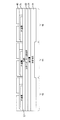
12 N型領域
13 半導体構造(GaN)
14 発光領域(III族窒化物発光層、発光層)
16 P型領域
18 接合層
20 支持基板
22 光学インピーダンス整合層
23 接合層
24 基板(第二基板、セラミック基板、波長変換基板、電気伝導基板、光変換層)
31 構造
32 第1金属層
33 P接点(金属P接点)
34 第2金属層
36 N接点
38 誘電体(誘電体層)
40、40a、40b 接合パッド
42、44、46 素子(半導体発光素子)
Claims (12)
- 成長基板上に成長された半導体構造を有するウエハを用意し、前記半導体構造は、N型領域とP型領域との間に挟まれたIII族窒化物発光層を有し、
前記ウエハを第2基板に接合し、前記第2基板は、透明であって、ガラス内に置かれた波長変換材料を有し、
前記成長基板を取り除き、
前記ウエハを前記第2基板に接合した後、前記ウエハを複数の発光素子へと処理し、該処理は、
前記P型領域上に金属接点を形成し、
前記N型領域の一部が見えるように、前記発光層と前記P型領域との一部を取り除き、且つ
前記発光層と前記P型領域との一部を取り除いたことにより露出した前記N型領域の上に金属接点を形成する
ことを有し、且つ
前記ウエハを複数の発光素子へと処理した後、且つ前記ウエハをダイシングする前に、前記ウエハを検査し且つ前記検査の結果に応じて前記発光素子夫々に対応する波長変換材料の量を調整する、
ことを有する方法。 - 前記第2基板は、1.5よりも高い屈折率を持つ、請求項1記載の方法。
- 前記調整することは、レーザーアブレーションにより波長変換材料を取り除くことを有する、請求項1記載の方法。
- 前記調整することは、波長変換材料を追加することを含む、請求項1記載の方法。
- 前記ウエハを第2基板に接合することは、前記ウエハと前記第2基板とを500℃よりも高い温度で押し付けることを有する、請求項1記載の方法。
- 前記調整することの後に、前記ウエハを、単一の発光ダイオードへ、又は発光ダイオードの群へとダイシングすることを更に有する請求項1記載の方法。
- 前記ウエハをダイシングした後に、前記単一の発光ダイオード又は前記発光ダイオードの群の各々の側面に、反射コーティングを形成することを更に有する請求項6記載の方法。
- 前記接合することよりも前に、光学インピーダンス整合層を前記半導体構造の上に形成することを更に有する請求項1記載の方法。
- 前記半導体構造に接合された面とは反対側の前記第2基板の表面をテクスチャー処理することを更に有する請求項1記載の方法。
- 前記ウエハを前記複数の発光素子へと処理することは、前記成長基板を取り除いた後に行われる、請求項1記載の方法。
- 当該方法はさらに、前記成長基板を取り除く前に、前記ウエハを支持基板に接合することを有し、前記ウエハを第2基板に接合することは、前記半導体構造が前記支持基板に接合されたまま、前記成長基板を取り除いた後に行われる、請求項1記載の方法。
- 前記第2基板に接合された面とは反対側の前記半導体構造の表面の上に、反射コンタクトを形成することを更に有する請求項1記載の方法。
Applications Claiming Priority (3)
| Application Number | Priority Date | Filing Date | Title |
|---|---|---|---|
| US201161527634P | 2011-08-26 | 2011-08-26 | |
| US61/527,634 | 2011-08-26 | ||
| PCT/IB2012/054225 WO2013030718A1 (en) | 2011-08-26 | 2012-08-21 | Method of processing a semiconductor structure |
Related Child Applications (1)
| Application Number | Title | Priority Date | Filing Date |
|---|---|---|---|
| JP2016142915A Division JP6294402B2 (ja) | 2011-08-26 | 2016-07-21 | 半導体構造の処理方法 |
Publications (2)
| Publication Number | Publication Date |
|---|---|
| JP2014525674A JP2014525674A (ja) | 2014-09-29 |
| JP6305337B2 true JP6305337B2 (ja) | 2018-04-04 |
Family
ID=47148861
Family Applications (2)
| Application Number | Title | Priority Date | Filing Date |
|---|---|---|---|
| JP2014526585A Active JP6305337B2 (ja) | 2011-08-26 | 2012-08-21 | 半導体構造の処理方法 |
| JP2016142915A Active JP6294402B2 (ja) | 2011-08-26 | 2016-07-21 | 半導体構造の処理方法 |
Family Applications After (1)
| Application Number | Title | Priority Date | Filing Date |
|---|---|---|---|
| JP2016142915A Active JP6294402B2 (ja) | 2011-08-26 | 2016-07-21 | 半導体構造の処理方法 |
Country Status (7)
| Country | Link |
|---|---|
| US (1) | US10056531B2 (ja) |
| EP (1) | EP2748864B1 (ja) |
| JP (2) | JP6305337B2 (ja) |
| KR (2) | KR102082499B1 (ja) |
| CN (1) | CN103748696B (ja) |
| TW (2) | TWI635628B (ja) |
| WO (1) | WO2013030718A1 (ja) |
Families Citing this family (16)
| Publication number | Priority date | Publication date | Assignee | Title |
|---|---|---|---|---|
| KR101911580B1 (ko) | 2011-07-15 | 2018-10-24 | 루미리즈 홀딩 비.브이. | 반도체 장치를 지지 기판에 접착시키는 방법 |
| WO2013118072A2 (en) | 2012-02-10 | 2013-08-15 | Koninklijke Philips N.V. | Wavelength converted light emitting device |
| US20180231191A1 (en) * | 2014-10-01 | 2018-08-16 | Koninklijke Philips N.V. | Light source with tunable emission spectrum |
| US10217914B2 (en) | 2015-05-27 | 2019-02-26 | Samsung Electronics Co., Ltd. | Semiconductor light emitting device |
| JP2017220479A (ja) * | 2016-06-03 | 2017-12-14 | 株式会社ディスコ | 発光ダイオードチップの製造方法 |
| JP2017224726A (ja) * | 2016-06-15 | 2017-12-21 | 株式会社ディスコ | 発光ダイオードチップの製造方法 |
| JP2017224728A (ja) * | 2016-06-15 | 2017-12-21 | 株式会社ディスコ | 発光ダイオードチップの製造方法 |
| JP2018014425A (ja) * | 2016-07-21 | 2018-01-25 | 株式会社ディスコ | 発光ダイオードチップの製造方法 |
| TWI759289B (zh) * | 2017-03-21 | 2022-04-01 | 晶元光電股份有限公司 | 發光元件 |
| US10559727B2 (en) * | 2017-07-25 | 2020-02-11 | Shenzhen China Star Optoelectronics Semiconductor Display Technology Co., Ltd. | Manufacturing method of colorful Micro-LED, display modlue and terminals |
| CN109461805B (zh) * | 2018-03-07 | 2021-08-10 | 普瑞光电股份有限公司 | 具有位于包含荧光体的玻璃转换板上的玻璃透镜的汽车led光源 |
| US11348906B2 (en) | 2018-03-21 | 2022-05-31 | Osram Opto Semiconductors Gmbh | Optoelectronic device comprising a phosphor plate and method of manufacturing the optoelectronic device |
| CN110544641A (zh) * | 2018-05-28 | 2019-12-06 | 山东浪潮华光光电子股份有限公司 | 一种发光二极管芯片的测试方法 |
| JP2019212875A (ja) * | 2018-06-08 | 2019-12-12 | 信越半導体株式会社 | 発光素子及び発光素子の製造方法 |
| JP7108196B2 (ja) | 2019-12-26 | 2022-07-28 | 日亜化学工業株式会社 | 発光装置、波長変換部材の製造方法及び発光装置の製造方法 |
| KR20210123064A (ko) * | 2020-04-02 | 2021-10-13 | 웨이브로드 주식회사 | 3족 질화물 반도체 소자를 제조하는 방법 |
Family Cites Families (27)
| Publication number | Priority date | Publication date | Assignee | Title |
|---|---|---|---|---|
| JP3230638B2 (ja) | 1993-02-10 | 2001-11-19 | シャープ株式会社 | 発光ダイオードの製造方法 |
| JP2002344029A (ja) | 2001-05-17 | 2002-11-29 | Rohm Co Ltd | 発光ダイオードの色調調整方法 |
| TWI231054B (en) * | 2003-03-13 | 2005-04-11 | Showa Denko Kk | Light-emitting diode and its manufacturing method |
| CN100459189C (zh) | 2003-11-19 | 2009-02-04 | 日亚化学工业株式会社 | 半导体元件 |
| JP4594708B2 (ja) * | 2003-12-05 | 2010-12-08 | 昭和電工株式会社 | 発光ダイオードおよびその製造方法、発光ダイオードランプ。 |
| JP2005259912A (ja) * | 2004-03-10 | 2005-09-22 | Shin Etsu Handotai Co Ltd | 発光素子の製造方法 |
| WO2005091390A1 (en) * | 2004-03-18 | 2005-09-29 | Showa Denko K.K. | Group iii nitride semiconductor light-emitting device and producing method thereof |
| JP4116587B2 (ja) * | 2004-04-13 | 2008-07-09 | 浜松ホトニクス株式会社 | 半導体発光素子及びその製造方法 |
| JP4857596B2 (ja) * | 2004-06-24 | 2012-01-18 | 豊田合成株式会社 | 発光素子の製造方法 |
| US7560294B2 (en) * | 2004-06-07 | 2009-07-14 | Toyoda Gosei Co., Ltd. | Light emitting element and method of making same |
| US7553683B2 (en) | 2004-06-09 | 2009-06-30 | Philips Lumiled Lighting Co., Llc | Method of forming pre-fabricated wavelength converting elements for semiconductor light emitting devices |
| KR100854986B1 (ko) * | 2004-06-11 | 2008-08-28 | 쇼와 덴코 가부시키가이샤 | 화합물 반도체 소자 웨이퍼의 제조방법 |
| JP4692059B2 (ja) * | 2005-04-25 | 2011-06-01 | パナソニック電工株式会社 | 発光装置の製造方法 |
| JP4895541B2 (ja) | 2005-07-08 | 2012-03-14 | シャープ株式会社 | 波長変換部材、発光装置及び波長変換部材の製造方法 |
| US7456080B2 (en) * | 2005-12-19 | 2008-11-25 | Corning Incorporated | Semiconductor on glass insulator made using improved ion implantation process |
| JP2008135697A (ja) | 2006-10-23 | 2008-06-12 | Rohm Co Ltd | 半導体発光素子 |
| US7521862B2 (en) | 2006-11-20 | 2009-04-21 | Philips Lumileds Lighting Co., Llc | Light emitting device including luminescent ceramic and light-scattering material |
| JP2008159628A (ja) | 2006-12-20 | 2008-07-10 | Rohm Co Ltd | 半導体発光素子及び半導体発光素子の製造方法 |
| US7989236B2 (en) | 2007-12-27 | 2011-08-02 | Toyoda Gosei Co., Ltd. | Method of making phosphor containing glass plate, method of making light emitting device |
| US8877524B2 (en) * | 2008-03-31 | 2014-11-04 | Cree, Inc. | Emission tuning methods and devices fabricated utilizing methods |
| US10147843B2 (en) | 2008-07-24 | 2018-12-04 | Lumileds Llc | Semiconductor light emitting device including a window layer and a light-directing structure |
| US8236582B2 (en) | 2008-07-24 | 2012-08-07 | Philips Lumileds Lighting Company, Llc | Controlling edge emission in package-free LED die |
| DE102008039790B4 (de) | 2008-08-26 | 2022-05-12 | OSRAM Opto Semiconductors Gesellschaft mit beschränkter Haftung | Optoelektronisches Bauelement und Verfahren zu dessen Herstellung |
| JP2010087292A (ja) * | 2008-09-30 | 2010-04-15 | Toyoda Gosei Co Ltd | 発光素子 |
| WO2010087292A1 (ja) | 2009-01-27 | 2010-08-05 | 三菱電機株式会社 | 送信装置、送受信装置、通信システム、および通信方法 |
| CN102361953A (zh) * | 2009-03-27 | 2012-02-22 | 柯尼卡美能达精密光学株式会社 | 荧光体部件、荧光体部件的制造方法以及照明装置 |
| US8581229B2 (en) | 2009-11-23 | 2013-11-12 | Koninklijke Philips N.V. | III-V light emitting device with thin n-type region |
-
2012
- 2012-08-21 KR KR1020197008997A patent/KR102082499B1/ko active IP Right Grant
- 2012-08-21 CN CN201280041603.5A patent/CN103748696B/zh active Active
- 2012-08-21 US US14/238,477 patent/US10056531B2/en active Active
- 2012-08-21 WO PCT/IB2012/054225 patent/WO2013030718A1/en active Application Filing
- 2012-08-21 KR KR1020147007513A patent/KR101965265B1/ko active Application Filing
- 2012-08-21 EP EP12784063.5A patent/EP2748864B1/en active Active
- 2012-08-21 JP JP2014526585A patent/JP6305337B2/ja active Active
- 2012-08-24 TW TW106103469A patent/TWI635628B/zh active
- 2012-08-24 TW TW101130877A patent/TWI583029B/zh active
-
2016
- 2016-07-21 JP JP2016142915A patent/JP6294402B2/ja active Active
Also Published As
| Publication number | Publication date |
|---|---|
| US20140179029A1 (en) | 2014-06-26 |
| EP2748864A1 (en) | 2014-07-02 |
| TWI583029B (zh) | 2017-05-11 |
| WO2013030718A1 (en) | 2013-03-07 |
| JP2016213490A (ja) | 2016-12-15 |
| TW201717436A (zh) | 2017-05-16 |
| CN103748696A (zh) | 2014-04-23 |
| JP2014525674A (ja) | 2014-09-29 |
| CN103748696B (zh) | 2018-06-22 |
| JP6294402B2 (ja) | 2018-03-14 |
| KR20190038671A (ko) | 2019-04-08 |
| TW201318229A (zh) | 2013-05-01 |
| KR20140053361A (ko) | 2014-05-07 |
| TWI635628B (zh) | 2018-09-11 |
| KR101965265B1 (ko) | 2019-04-04 |
| KR102082499B1 (ko) | 2020-02-27 |
| US10056531B2 (en) | 2018-08-21 |
| EP2748864B1 (en) | 2020-02-05 |
Similar Documents
| Publication | Publication Date | Title |
|---|---|---|
| JP6294402B2 (ja) | 半導体構造の処理方法 | |
| TWI734110B (zh) | 照明結構及製造發光裝置之方法 | |
| CN111509112B (zh) | 波长转换的半导体发光器件 | |
| JP6419077B2 (ja) | 波長変換発光デバイス | |
| EP2984685B1 (en) | Fabrication method for top emitting semiconductor light emitting devices | |
| JP6535598B2 (ja) | フィルタ及び保護層を含む発光デバイス | |
| JP7361810B2 (ja) | 反射層を伴うマウント上の発光デバイス | |
| JP6462029B2 (ja) | 基板を半導体発光素子に接合する方法 | |
| EP2831930B1 (en) | Sealed semiconductor light emitting device and method of forming thereof | |
| TWI462241B (zh) | 高熱傳導性光電元件 |
Legal Events
| Date | Code | Title | Description |
|---|---|---|---|
| A621 | Written request for application examination |
Free format text: JAPANESE INTERMEDIATE CODE: A621 Effective date: 20150819 |
|
| A977 | Report on retrieval |
Free format text: JAPANESE INTERMEDIATE CODE: A971007 Effective date: 20160420 |
|
| A131 | Notification of reasons for refusal |
Free format text: JAPANESE INTERMEDIATE CODE: A131 Effective date: 20160426 |
|
| A521 | Request for written amendment filed |
Free format text: JAPANESE INTERMEDIATE CODE: A523 Effective date: 20160721 |
|
| A131 | Notification of reasons for refusal |
Free format text: JAPANESE INTERMEDIATE CODE: A131 Effective date: 20161220 |
|
| A521 | Request for written amendment filed |
Free format text: JAPANESE INTERMEDIATE CODE: A523 Effective date: 20170317 |
|
| A131 | Notification of reasons for refusal |
Free format text: JAPANESE INTERMEDIATE CODE: A131 Effective date: 20170815 |
|
| A601 | Written request for extension of time |
Free format text: JAPANESE INTERMEDIATE CODE: A601 Effective date: 20171113 |
|
| A521 | Request for written amendment filed |
Free format text: JAPANESE INTERMEDIATE CODE: A523 Effective date: 20180117 |
|
| TRDD | Decision of grant or rejection written | ||
| A01 | Written decision to grant a patent or to grant a registration (utility model) |
Free format text: JAPANESE INTERMEDIATE CODE: A01 Effective date: 20180206 |
|
| A61 | First payment of annual fees (during grant procedure) |
Free format text: JAPANESE INTERMEDIATE CODE: A61 Effective date: 20180306 |
|
| R150 | Certificate of patent or registration of utility model |
Ref document number: 6305337 Country of ref document: JP Free format text: JAPANESE INTERMEDIATE CODE: R150 |
|
| S111 | Request for change of ownership or part of ownership |
Free format text: JAPANESE INTERMEDIATE CODE: R313113 |
|
| R350 | Written notification of registration of transfer |
Free format text: JAPANESE INTERMEDIATE CODE: R350 |
|
| R250 | Receipt of annual fees |
Free format text: JAPANESE INTERMEDIATE CODE: R250 |
|
| R250 | Receipt of annual fees |
Free format text: JAPANESE INTERMEDIATE CODE: R250 |
|
| R250 | Receipt of annual fees |
Free format text: JAPANESE INTERMEDIATE CODE: R250 |
|
| R250 | Receipt of annual fees |
Free format text: JAPANESE INTERMEDIATE CODE: R250 |