JP6263747B2 - 画像表示装置および画像表示装置の製造方法 - Google Patents
画像表示装置および画像表示装置の製造方法 Download PDFInfo
- Publication number
- JP6263747B2 JP6263747B2 JP2016509619A JP2016509619A JP6263747B2 JP 6263747 B2 JP6263747 B2 JP 6263747B2 JP 2016509619 A JP2016509619 A JP 2016509619A JP 2016509619 A JP2016509619 A JP 2016509619A JP 6263747 B2 JP6263747 B2 JP 6263747B2
- Authority
- JP
- Japan
- Prior art keywords
- frame member
- display panel
- bent piece
- front surface
- image display
- Prior art date
- Legal status (The legal status is an assumption and is not a legal conclusion. Google has not performed a legal analysis and makes no representation as to the accuracy of the status listed.)
- Active
Links
Images


Classifications
-
- G—PHYSICS
- G02—OPTICS
- G02F—OPTICAL DEVICES OR ARRANGEMENTS FOR THE CONTROL OF LIGHT BY MODIFICATION OF THE OPTICAL PROPERTIES OF THE MEDIA OF THE ELEMENTS INVOLVED THEREIN; NON-LINEAR OPTICS; FREQUENCY-CHANGING OF LIGHT; OPTICAL LOGIC ELEMENTS; OPTICAL ANALOGUE/DIGITAL CONVERTERS
- G02F1/00—Devices or arrangements for the control of the intensity, colour, phase, polarisation or direction of light arriving from an independent light source, e.g. switching, gating or modulating; Non-linear optics
- G02F1/01—Devices or arrangements for the control of the intensity, colour, phase, polarisation or direction of light arriving from an independent light source, e.g. switching, gating or modulating; Non-linear optics for the control of the intensity, phase, polarisation or colour
- G02F1/13—Devices or arrangements for the control of the intensity, colour, phase, polarisation or direction of light arriving from an independent light source, e.g. switching, gating or modulating; Non-linear optics for the control of the intensity, phase, polarisation or colour based on liquid crystals, e.g. single liquid crystal display cells
- G02F1/133—Constructional arrangements; Operation of liquid crystal cells; Circuit arrangements
- G02F1/1333—Constructional arrangements; Manufacturing methods
- G02F1/133308—Support structures for LCD panels, e.g. frames or bezels
-
- H—ELECTRICITY
- H05—ELECTRIC TECHNIQUES NOT OTHERWISE PROVIDED FOR
- H05K—PRINTED CIRCUITS; CASINGS OR CONSTRUCTIONAL DETAILS OF ELECTRIC APPARATUS; MANUFACTURE OF ASSEMBLAGES OF ELECTRICAL COMPONENTS
- H05K5/00—Casings, cabinets or drawers for electric apparatus
- H05K5/02—Details
- H05K5/0217—Mechanical details of casings
-
- H—ELECTRICITY
- H10—SEMICONDUCTOR DEVICES; ELECTRIC SOLID-STATE DEVICES NOT OTHERWISE PROVIDED FOR
- H10K—ORGANIC ELECTRIC SOLID-STATE DEVICES
- H10K50/00—Organic light-emitting devices
- H10K50/80—Constructional details
- H10K50/84—Passivation; Containers; Encapsulations
-
- H—ELECTRICITY
- H10—SEMICONDUCTOR DEVICES; ELECTRIC SOLID-STATE DEVICES NOT OTHERWISE PROVIDED FOR
- H10K—ORGANIC ELECTRIC SOLID-STATE DEVICES
- H10K2102/00—Constructional details relating to the organic devices covered by this subclass
- H10K2102/301—Details of OLEDs
- H10K2102/351—Thickness
Landscapes
- Physics & Mathematics (AREA)
- Nonlinear Science (AREA)
- Optics & Photonics (AREA)
- Mathematical Physics (AREA)
- Chemical & Material Sciences (AREA)
- Crystallography & Structural Chemistry (AREA)
- General Physics & Mathematics (AREA)
- Engineering & Computer Science (AREA)
- Microelectronics & Electronic Packaging (AREA)
- Devices For Indicating Variable Information By Combining Individual Elements (AREA)
- Electroluminescent Light Sources (AREA)
- Liquid Crystal (AREA)
Description
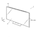
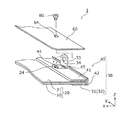
図1は、実施の形態における画像表示装置1の外観斜視図である。
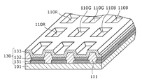
図3は、実施の形態における表示パネル10の一部切り欠き斜視図である。
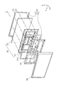
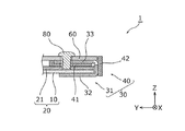
図6は、実施の形態における画像表示装置1の一部の構造を示す第1の分解斜視図であり、図7は、同構造を示す第2の分解斜視図である。
以上のように、本実施の形態の画像表示装置1は、表示ユニット20と、第一枠部材31とを備える。表示ユニット20は、表示パネル10とシャーシ21とを有する。第一枠部材31は、表示パネル10の前面周縁に配置される前面部32と、前面部32に接続された折曲片部33とを有する。折曲片部33は、前面部32が表示パネル10の前面に沿った状態で、シャーシ21の背面の方向に折り曲げられる。
図10は、実施の形態の変形例1における第一枠部材31の取り付け構造を示す部分断面図である。
図11は、実施の形態の変形例2における第一枠部材31の取り付け構造を示す部分断面図である。
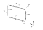
図12は、実施の形態の変形例3における第一枠部材37の構成例を示す斜視図である。
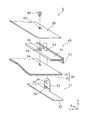
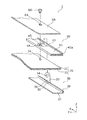
図13は、実施の形態の変形例4における画像表示装置1の一部の構造を示す分解斜視図である。
以上のように、本出願において開示する技術の例示として、実施の形態および変形例を説明した。しかしながら、本開示における技術は、これらに限定されず、適宜、変更、置き換え、付加、省略などを行った実施の形態にも適用可能である。また、上記実施の形態および変形例で説明した各構成要素を組み合わせて、新たな実施の形態とすることも可能である。そこで、以下、他の実施の形態を例示する。
10 表示パネル
20 表示ユニット
21 シャーシ
21a 凸部
24、34、44、64、64a ねじ孔
30 枠部材
31、31a、31b、31c、31d、37、39 第一枠部材
32 前面部
33 折曲片部
35 溝
36 貫通孔
38、42、42a、61 側面部
40 第二枠部材
41 背面部
43 取付孔
45 凹部
50、51 回路基板
60 バックカバー
101 TFT基板
110 画素
110B、110G、110R サブ画素
111 バンク
120 画素回路
130 有機EL素子
131 陽極
132 EL層
133 陰極
140 ゲート配線
150 ソース配線
160 電源配線
Claims (9)
- 前面に画像を表示する表示パネル、および、前記表示パネルの背面側に配置され、前記表示パネルを保持するシャーシを有する表示ユニットと、
前記表示パネルの前面周縁の少なくとも一部に沿って配置される第一枠部材とを備え、
前記第一枠部材は、前記表示パネルの前面に沿って配置される前面部と、前記前面部に接続された折曲片部であって、折り曲げられることで、前記前面部とは反対側の端部が前記シャーシの背面の側に配置された折曲片部とを有し、
さらに、前記表示ユニットを挟んで前記第一枠部材の前記前面部と対向する位置に配置された背面部を有する第二枠部材を備え、
前記第一枠部材の前記折曲片部は、前記第二枠部材に形成された取付孔を貫通した状態で折り曲げられている
画像表示装置。 - 前記取付孔は前記背面部に形成されており、
前記第二枠部材はさらに、前記取付孔の外側に配置され、前記折曲片部の少なくとも一部を覆うように設けられた側面部を有する
請求項1記載の画像表示装置。 - 前記折曲片部は、折り曲げられた状態で、ねじによって前記シャーシと締結されている
請求項1または2に記載の画像表示装置。 - さらに、前記シャーシの前記背面を覆うように配置されたバックカバーを備え、
前記バックカバーは、前記折曲片部とともに、前記ねじによって前記シャーシと締結されている
請求項3記載の画像表示装置。 - 前記第一枠部材は、前記表示パネルの前面周縁の全域に沿って配置された環状の部材であり、前記折曲片部を複数有する
請求項1〜4のいずれか1項に記載の画像表示装置。 - 前記表示パネルは前面視において矩形であり、
前記第一枠部材は前記表示パネルの4辺に沿って配置された角環状の部材であり、
前記折曲片部は、前記第一枠部材における前記4辺のそれぞれに対応する部分に少なくとも1つ配置されている
請求項5記載の画像表示装置。 - さらに、前記シャーシの前記背面、および、前記第一枠部材の前記折曲片部を覆うように配置されたバックカバーを備える
請求項1〜3のいずれか1項に記載の画像表示装置。 - 前記表示パネルは、有機EL(Electro Luminescence)ディスプレイパネルである
請求項1〜7のいずれか1項に記載の画像表示装置。 - 画像表示装置の製造方法であって、
前記画像表示装置は、
前面に画像を表示する表示パネル、および、前記表示パネルの背面側に配置され、前記表示パネルを保持するシャーシを有する表示ユニットと、前記表示パネルの前面周縁の少なくとも一部に沿って配置される第一枠部材と、
前記表示ユニットを挟んで前記第一枠部材の前記前面部と対向する位置に配置された背面部を有する第二枠部材とを備え、
前記第一枠部材は、前面部と前記前面部に接続された折曲片部とを有し、
前記製造方法は、
前記前面部を、前記表示パネルの前面に沿って配置する配置工程と、
前記前面部が前記表示パネルの前面に沿って配置された状態で、前記折曲片部を前記シャーシの背面の方向に折り曲げる折曲工程とを含み、
前記折曲工程では、前記折曲片部は、前記第二枠部材に形成された取付孔を貫通した状態で折り曲げられる
画像表示装置の製造方法。
Applications Claiming Priority (3)
| Application Number | Priority Date | Filing Date | Title |
|---|---|---|---|
| JP2014064664 | 2014-03-26 | ||
| JP2014064664 | 2014-03-26 | ||
| PCT/JP2014/006361 WO2015145510A1 (ja) | 2014-03-26 | 2014-12-22 | 画像表示装置および画像表示装置の製造方法 |
Publications (2)
| Publication Number | Publication Date |
|---|---|
| JPWO2015145510A1 JPWO2015145510A1 (ja) | 2017-04-13 |
| JP6263747B2 true JP6263747B2 (ja) | 2018-01-24 |
Family
ID=54194112
Family Applications (1)
| Application Number | Title | Priority Date | Filing Date |
|---|---|---|---|
| JP2016509619A Active JP6263747B2 (ja) | 2014-03-26 | 2014-12-22 | 画像表示装置および画像表示装置の製造方法 |
Country Status (3)
| Country | Link |
|---|---|
| US (1) | US10098244B2 (ja) |
| JP (1) | JP6263747B2 (ja) |
| WO (1) | WO2015145510A1 (ja) |
Families Citing this family (7)
| Publication number | Priority date | Publication date | Assignee | Title |
|---|---|---|---|---|
| CN104820305B (zh) * | 2015-05-19 | 2018-12-11 | 深圳市华星光电技术有限公司 | 显示装置 |
| KR102357930B1 (ko) * | 2017-08-30 | 2022-02-03 | 엘지디스플레이 주식회사 | 디스플레이 장치 |
| JP6585685B2 (ja) * | 2017-10-31 | 2019-10-02 | ファナック株式会社 | 表示器付き制御装置 |
| WO2020103143A1 (zh) * | 2018-11-23 | 2020-05-28 | 深圳市光祥科技股份有限公司 | Led显示单元 |
| KR20220147770A (ko) * | 2021-04-27 | 2022-11-04 | 삼성디스플레이 주식회사 | 표시 장치 및 표시 장치의 제어방법 |
| WO2023286886A1 (ko) * | 2021-07-14 | 2023-01-19 | 엘지전자 주식회사 | 디스플레이 디바이스 |
| JP7399591B2 (ja) * | 2021-10-11 | 2023-12-18 | 矢崎総業株式会社 | 表示装置 |
Family Cites Families (14)
| Publication number | Priority date | Publication date | Assignee | Title |
|---|---|---|---|---|
| JPS6429624A (en) | 1987-07-23 | 1989-01-31 | Toshiba Corp | Combined cycle power generation plant for coal gasification |
| JPS6429624U (ja) * | 1987-08-13 | 1989-02-22 | ||
| US6480245B1 (en) | 1999-03-26 | 2002-11-12 | Advanced Display Inc. | LCD in which lamp reflector is grounded to panel housing via screw, pinch fastening, or snap pressing means |
| JPWO2004111977A1 (ja) | 2003-06-13 | 2006-07-27 | 東芝松下ディスプレイテクノロジー株式会社 | 平面表示装置 |
| JP2006162985A (ja) | 2004-12-07 | 2006-06-22 | Toshiba Corp | 表示装置 |
| JPWO2007083500A1 (ja) * | 2006-01-23 | 2009-06-11 | 日本板硝子株式会社 | アンテナ付き画像表示装置 |
| JP5028035B2 (ja) | 2006-06-29 | 2012-09-19 | パナソニック株式会社 | 画像表示装置 |
| JP2008116523A (ja) * | 2006-11-01 | 2008-05-22 | Sony Corp | 表示機器および表示パネル |
| US8797473B2 (en) * | 2007-09-12 | 2014-08-05 | Japan Display West Inc. | Electro-optical device having a frame including a conduction part and a resin part |
| JP5546136B2 (ja) * | 2009-02-03 | 2014-07-09 | キヤノン株式会社 | 画像表示装置 |
| JP4659156B1 (ja) * | 2010-07-01 | 2011-03-30 | オリオン電機株式会社 | 液晶表示パネルを備えた電子機器 |
| CN102393578B (zh) * | 2011-12-02 | 2014-05-21 | 深圳市华星光电技术有限公司 | 液晶显示装置及其机壳 |
| DE112012006239B4 (de) * | 2012-04-18 | 2016-02-25 | Mitsubishi Electric Corporation | Elektronische Vorrichtung |
| TWI481330B (zh) * | 2013-04-10 | 2015-04-11 | 瑞軒科技股份有限公司 | 顯示裝置 |
-
2014
- 2014-12-22 WO PCT/JP2014/006361 patent/WO2015145510A1/ja not_active Ceased
- 2014-12-22 JP JP2016509619A patent/JP6263747B2/ja active Active
- 2014-12-22 US US15/127,928 patent/US10098244B2/en active Active
Also Published As
| Publication number | Publication date |
|---|---|
| WO2015145510A1 (ja) | 2015-10-01 |
| US10098244B2 (en) | 2018-10-09 |
| US20170094813A1 (en) | 2017-03-30 |
| JPWO2015145510A1 (ja) | 2017-04-13 |
Similar Documents
| Publication | Publication Date | Title |
|---|---|---|
| JP6263747B2 (ja) | 画像表示装置および画像表示装置の製造方法 | |
| KR101035502B1 (ko) | 발광다이오드를 이용한 액정표시장치모듈 | |
| KR101189135B1 (ko) | 액정표시장치모듈 | |
| US8905615B2 (en) | Light source module and display device having the same | |
| US20150212261A1 (en) | Lighting apparatus, display apparatus, and television receiver | |
| US9838766B2 (en) | Speaker and microphone integrated display panel | |
| KR20130078656A (ko) | 디스플레이 장치 | |
| US9033567B2 (en) | Backlight assembly | |
| KR102262773B1 (ko) | 가변형 표시장치 | |
| US20180107048A1 (en) | Display module and display device | |
| KR101633113B1 (ko) | 액정표시장치 | |
| US20210110782A1 (en) | Display Device and Driving Method Thereof | |
| WO2015087462A1 (ja) | 有機el表示装置、支持台、および画像表示装置 | |
| US11106087B2 (en) | Lighting device having light sources arranged in columns and display device thereof | |
| KR102902146B1 (ko) | 발광 다이오드 모듈 및 이를 포함하는 디스플레이 장치 | |
| JP5576945B2 (ja) | 表示装置 | |
| WO2018225432A1 (ja) | 表示装置および電子機器 | |
| US8179683B2 (en) | Display device | |
| JP2013218922A (ja) | バックライト装置、表示装置、及びテレビ受信装置 | |
| KR102319801B1 (ko) | 디스플레이 장치 | |
| JP6213578B2 (ja) | 有機elパネルユニットおよび有機el表示装置 | |
| KR102217995B1 (ko) | 가변형 표시장치 | |
| KR20060081590A (ko) | 회로부 커버용 케이스를 갖는 평판표시장치 | |
| KR102053640B1 (ko) | 디스플레이 장치 | |
| WO2015087463A1 (ja) | 有機el表示装置 |
Legal Events
| Date | Code | Title | Description |
|---|---|---|---|
| A131 | Notification of reasons for refusal |
Free format text: JAPANESE INTERMEDIATE CODE: A131 Effective date: 20170725 |
|
| A521 | Request for written amendment filed |
Free format text: JAPANESE INTERMEDIATE CODE: A523 Effective date: 20170922 |
|
| TRDD | Decision of grant or rejection written | ||
| A01 | Written decision to grant a patent or to grant a registration (utility model) |
Free format text: JAPANESE INTERMEDIATE CODE: A01 Effective date: 20171107 |
|
| A61 | First payment of annual fees (during grant procedure) |
Free format text: JAPANESE INTERMEDIATE CODE: A61 Effective date: 20171120 |
|
| R150 | Certificate of patent or registration of utility model |
Ref document number: 6263747 Country of ref document: JP Free format text: JAPANESE INTERMEDIATE CODE: R150 |
|
| R250 | Receipt of annual fees |
Free format text: JAPANESE INTERMEDIATE CODE: R250 |
|
| R250 | Receipt of annual fees |
Free format text: JAPANESE INTERMEDIATE CODE: R250 |
|
| R250 | Receipt of annual fees |
Free format text: JAPANESE INTERMEDIATE CODE: R250 |
|
| S303 | Written request for registration of pledge or change of pledge |
Free format text: JAPANESE INTERMEDIATE CODE: R316303 |
|
| R350 | Written notification of registration of transfer |
Free format text: JAPANESE INTERMEDIATE CODE: R350 |
|
| S803 | Written request for registration of cancellation of provisional registration |
Free format text: JAPANESE INTERMEDIATE CODE: R316803 |
|
| R350 | Written notification of registration of transfer |
Free format text: JAPANESE INTERMEDIATE CODE: R350 |
|
| R250 | Receipt of annual fees |
Free format text: JAPANESE INTERMEDIATE CODE: R250 |
|
| S111 | Request for change of ownership or part of ownership |
Free format text: JAPANESE INTERMEDIATE CODE: R313113 |
|
| R350 | Written notification of registration of transfer |
Free format text: JAPANESE INTERMEDIATE CODE: R350 |
|
| R250 | Receipt of annual fees |
Free format text: JAPANESE INTERMEDIATE CODE: R250 |