JP6146983B2 - 半導体メモリ装置 - Google Patents
半導体メモリ装置 Download PDFInfo
- Publication number
- JP6146983B2 JP6146983B2 JP2012234259A JP2012234259A JP6146983B2 JP 6146983 B2 JP6146983 B2 JP 6146983B2 JP 2012234259 A JP2012234259 A JP 2012234259A JP 2012234259 A JP2012234259 A JP 2012234259A JP 6146983 B2 JP6146983 B2 JP 6146983B2
- Authority
- JP
- Japan
- Prior art keywords
- bit line
- potential
- selection transistor
- inverter
- switch
- Prior art date
- Legal status (The legal status is an assumption and is not a legal conclusion. Google has not performed a legal analysis and makes no representation as to the accuracy of the status listed.)
- Expired - Fee Related
Links
- 239000004065 semiconductor Substances 0.000 title claims description 58
- 230000015654 memory Effects 0.000 claims description 127
- 239000003990 capacitor Substances 0.000 description 34
- 239000012212 insulator Substances 0.000 description 29
- 238000000034 method Methods 0.000 description 27
- 239000011229 interlayer Substances 0.000 description 19
- 230000003321 amplification Effects 0.000 description 11
- 239000010410 layer Substances 0.000 description 11
- 238000003199 nucleic acid amplification method Methods 0.000 description 11
- 230000008569 process Effects 0.000 description 10
- 230000010354 integration Effects 0.000 description 9
- 239000000758 substrate Substances 0.000 description 9
- 238000007599 discharging Methods 0.000 description 8
- 238000011084 recovery Methods 0.000 description 6
- 230000007423 decrease Effects 0.000 description 4
- 230000006870 function Effects 0.000 description 4
- 230000007257 malfunction Effects 0.000 description 4
- 230000000694 effects Effects 0.000 description 3
- 230000003071 parasitic effect Effects 0.000 description 3
- XUIMIQQOPSSXEZ-UHFFFAOYSA-N Silicon Chemical compound [Si] XUIMIQQOPSSXEZ-UHFFFAOYSA-N 0.000 description 2
- 230000008859 change Effects 0.000 description 2
- 239000013078 crystal Substances 0.000 description 2
- 238000013461 design Methods 0.000 description 2
- 238000010586 diagram Methods 0.000 description 2
- 238000002955 isolation Methods 0.000 description 2
- 238000004519 manufacturing process Methods 0.000 description 2
- 229910052710 silicon Inorganic materials 0.000 description 2
- 239000010703 silicon Substances 0.000 description 2
- 230000003213 activating effect Effects 0.000 description 1
- 230000004913 activation Effects 0.000 description 1
- 238000013459 approach Methods 0.000 description 1
- 230000015572 biosynthetic process Effects 0.000 description 1
- 230000000295 complement effect Effects 0.000 description 1
- 239000002019 doping agent Substances 0.000 description 1
- 230000005669 field effect Effects 0.000 description 1
- 239000012535 impurity Substances 0.000 description 1
- 230000014759 maintenance of location Effects 0.000 description 1
- 230000013011 mating Effects 0.000 description 1
- 239000011159 matrix material Substances 0.000 description 1
- 238000012545 processing Methods 0.000 description 1
- 230000009467 reduction Effects 0.000 description 1
- 238000012546 transfer Methods 0.000 description 1
Images


Classifications
-
- G—PHYSICS
- G11—INFORMATION STORAGE
- G11C—STATIC STORES
- G11C5/00—Details of stores covered by group G11C11/00
- G11C5/06—Arrangements for interconnecting storage elements electrically, e.g. by wiring
-
- G—PHYSICS
- G11—INFORMATION STORAGE
- G11C—STATIC STORES
- G11C11/00—Digital stores characterised by the use of particular electric or magnetic storage elements; Storage elements therefor
- G11C11/21—Digital stores characterised by the use of particular electric or magnetic storage elements; Storage elements therefor using electric elements
- G11C11/34—Digital stores characterised by the use of particular electric or magnetic storage elements; Storage elements therefor using electric elements using semiconductor devices
- G11C11/40—Digital stores characterised by the use of particular electric or magnetic storage elements; Storage elements therefor using electric elements using semiconductor devices using transistors
- G11C11/401—Digital stores characterised by the use of particular electric or magnetic storage elements; Storage elements therefor using electric elements using semiconductor devices using transistors forming cells needing refreshing or charge regeneration, i.e. dynamic cells
- G11C11/4063—Auxiliary circuits, e.g. for addressing, decoding, driving, writing, sensing or timing
- G11C11/407—Auxiliary circuits, e.g. for addressing, decoding, driving, writing, sensing or timing for memory cells of the field-effect type
- G11C11/409—Read-write [R-W] circuits
- G11C11/4094—Bit-line management or control circuits
-
- G—PHYSICS
- G11—INFORMATION STORAGE
- G11C—STATIC STORES
- G11C11/00—Digital stores characterised by the use of particular electric or magnetic storage elements; Storage elements therefor
- G11C11/21—Digital stores characterised by the use of particular electric or magnetic storage elements; Storage elements therefor using electric elements
- G11C11/34—Digital stores characterised by the use of particular electric or magnetic storage elements; Storage elements therefor using electric elements using semiconductor devices
- G11C11/40—Digital stores characterised by the use of particular electric or magnetic storage elements; Storage elements therefor using electric elements using semiconductor devices using transistors
- G11C11/401—Digital stores characterised by the use of particular electric or magnetic storage elements; Storage elements therefor using electric elements using semiconductor devices using transistors forming cells needing refreshing or charge regeneration, i.e. dynamic cells
- G11C11/4063—Auxiliary circuits, e.g. for addressing, decoding, driving, writing, sensing or timing
- G11C11/407—Auxiliary circuits, e.g. for addressing, decoding, driving, writing, sensing or timing for memory cells of the field-effect type
- G11C11/409—Read-write [R-W] circuits
- G11C11/4097—Bit-line organisation, e.g. bit-line layout, folded bit lines
-
- G—PHYSICS
- G11—INFORMATION STORAGE
- G11C—STATIC STORES
- G11C7/00—Arrangements for writing information into, or reading information out from, a digital store
- G11C7/02—Arrangements for writing information into, or reading information out from, a digital store with means for avoiding parasitic signals
-
- G—PHYSICS
- G11—INFORMATION STORAGE
- G11C—STATIC STORES
- G11C2207/00—Indexing scheme relating to arrangements for writing information into, or reading information out from, a digital store
- G11C2207/002—Isolation gates, i.e. gates coupling bit lines to the sense amplifier
-
- G—PHYSICS
- G11—INFORMATION STORAGE
- G11C—STATIC STORES
- G11C2207/00—Indexing scheme relating to arrangements for writing information into, or reading information out from, a digital store
- G11C2207/005—Transfer gates, i.e. gates coupling the sense amplifier output to data lines, I/O lines or global bit lines
Landscapes
- Engineering & Computer Science (AREA)
- Microelectronics & Electronic Packaging (AREA)
- Computer Hardware Design (AREA)
- Dram (AREA)
- Semiconductor Memories (AREA)
Description
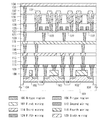
図1(A)、図1(B)および図4(A)に本実施の形態の半導体メモリ装置の一例を示す。図1(A)には、メモリブロックMB_n_m、メモリブロックMB_n+1_mとそれらの接続するビット線BL_m、第1選択線SL1_n、第1選択線SL1_n+1、ワード線WL_n_1乃至ワード線WL_n_4、ワード線WL_n+1_1乃至ワード線WL_n+1_4が示されている。
図2に本実施の形態の半導体メモリ装置の一例を示す。図2には、メモリブロックMB_n_m、メモリブロックMB_n_m+1、メモリブロックMB_n+1_m、メモリブロックMB_n+1_m+1とそれらの接続するビット線BL_m、ビット線BL_m+1、第1選択線SL1_n、第1選択線SL1_n+1、ワード線WL_n_1乃至ワード線WL_n_4、ワード線WL_n+1_1乃至ワード線WL_n+1_4が示されている。メモリブロックMBとしては、図1(B)に示される構成のものを用いてもよい。
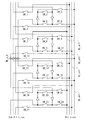
図3に本実施の形態の半導体メモリ装置の一例を示す。本実施の形態の半導体メモリ装置は、図2の半導体メモリ装置で4つ必要であった第2選択トランジスタSTr2を2つとしたものである。2つの第2選択トランジスタSTr2は同期して動作する。
本実施の形態では、本発明の一態様の半導体メモリ装置の例について図8、図9(A)乃至図9(C)、図10(A)乃至図10(C)および図11を用いて説明する。なお、本実施の形態では、同じハッチングの部分は同じ種類のものを示す。
実施の形態1および実施の形態4では、サブビット線をプリチャージする際や、サブビット線に接続するメモリセルにデータを書き込む際に、第1選択トランジスタを用いたが、第1選択トランジスタを用いずとも、サブビット線をプリチャージすることや、サブビット線に接続するメモリセルにデータを書き込むことができる。用いる増幅回路は図4(A)に示されるものである。
本実施の形態でも、実施の形態5と同様に第1選択トランジスタを有しないメモリブロックを用いた半導体メモリ装置の駆動方法の例について説明する。以下、その場合の駆動方法の例について説明する。なお、用いる半導体メモリ装置は、増幅回路として図4(A)に示される回路を用いた図1(A)の構成の回路(ただし、第1選択トランジスタSTr1を有しない)である。メモリブロックMB_n_mの中の1つのメモリセルのデータの読み出しとデータの回復、あるいはデータの書き換えについて説明する。
実施の形態5と同様に、第2選択トランジスタSTr2_n_mと第3選択トランジスタSTr3_n_mをオンとし、サブビット線SBL_n_mをビット線BL_mの電位でプリチャージする。インバータINV_n+1_mは非アクティブ(すなわち、インバータの2つの電源電位をともに+0.5V)としておく。プリチャージ完了後、第3選択トランジスタSTr3_n_mをオフとする。
第3選択トランジスタSTr3_n+1_mをオンとして、インバータINV_n_mとインバータINV_n+1_mをアクティブとすることにより、サブビット線SBL_n_m−>インバータINV_n_m−>第3選択トランジスタSTr3_n+1_m−>第2選択トランジスタSTr2_n_m−>ビット線BL_mというルートを形成する。
データを回復する場合には、第2選択トランジスタSTr2_n_mをオンとし、また、インバータINV_n_mとインバータINV_n+1_mをアクティブとする。この際、ビット線BL_mとサブビット線SBL_n+1_mの電位の差が増幅され、サブビット線SBL_n+1_mの電位は、ビット線BL_mおよびサブビット線SBL_n_mの電位とは逆の位相の電位となる。
データを書き換える場合は、ビット線BL_mの電位をデータに応じた電位とした上で、第2選択トランジスタSTr2_n_mをオンとし、また、インバータINV_n_mとインバータINV_n+1_mをアクティブとする。この結果、サブビット線SBL_n_mの電位はビット線BL_mの電位(すなわち、書き換えるデータに応じた電位)と同じであり、データを読み出したメモリセルのトランジスタはオン状態を保っているので、その容量素子はビット線BL_mの電位で充電され、データが書き換えられる。
102 P型ウェル
103 N型ウェル
104 素子分離絶縁物
105 N型領域
106 P型領域
107 第1配線
108 第1層間絶縁物
109 第1コンタクトプラグ
110 第2配線
111 第1埋め込み絶縁物
112 第2層間絶縁物
113 第2コンタクトプラグ
114 第3配線
115 第2埋め込み絶縁物
116 第3層間絶縁物
117 第3コンタクトプラグ
118 第4配線
119 第3埋め込み絶縁物
120 第4層間絶縁物
121 第4コンタクトプラグ
122 半導体層
123 ゲート絶縁物
124 第5配線
125 第5層間絶縁物
126 第5コンタクトプラグ
127 第6層間絶縁物
128 第6コンタクトプラグ
129 第6配線
130 誘電体膜
131 第7配線
132 第7層間絶縁物
133 第7コンタクトプラグ
134 第8配線
AMP 増幅回路
BL ビット線
INV インバータ
MB メモリブロック
SBL サブビット線
SL1 第1選択線
SL2 第2選択線
SL3 第3選択線
SL4 第4選択線
STr1 第1選択トランジスタ
STr2 第2選択トランジスタ
STr3 第3選択トランジスタ
STr4 第4選択トランジスタ
SW スイッチ
WL ワード線
Claims (3)
- ビット線と、第1および第2のメモリブロックと、第1および第2のインバータとを有し、
前記第1および第2のメモリブロックは、それぞれ対応する第1および第2のサブビット線を有し、
前記第1のインバータの入力端子は、第1および第2のトランジスタを介して、前記ビット線と電気的に接続され、
前記第1のインバータの入力端子は、前記第1のサブビット線と電気的に接続され、
前記第1のインバータの入力端子は、前記第1のトランジスタを介して、前記第2のインバータの出力端子と電気的に接続され、
前記第1のインバータの出力端子は、第3のトランジスタを介して、前記ビット線と電気的に接続され、
前記第1のインバータの出力端子は、第4のトランジスタを介して、前記第2のサブビット線と電気的に接続され、
前記第1のインバータの出力端子は、前記第4のトランジスタを介して、前記第2のインバータの入力端子と電気的に接続されていることを特徴とする半導体メモリ装置。 - 請求項1において、
前記第1のトランジスタ又は前記第4のトランジスタの一方のみがオンとなる期間を有し、
前記期間において、前記第2のトランジスタ又は前記第3のトランジスタの少なくとも一方がオンとなることを特徴とする半導体メモリ装置。 - 請求項1又は請求項2において、
前記第1のメモリブロックが有するトランジスタは、前記第2のメモリブロックが有するトランジスタとは異なる層に設けられていることを特徴とする半導体メモリ装置。
Priority Applications (1)
| Application Number | Priority Date | Filing Date | Title |
|---|---|---|---|
| JP2012234259A JP6146983B2 (ja) | 2011-10-24 | 2012-10-24 | 半導体メモリ装置 |
Applications Claiming Priority (3)
| Application Number | Priority Date | Filing Date | Title |
|---|---|---|---|
| JP2011232372 | 2011-10-24 | ||
| JP2011232372 | 2011-10-24 | ||
| JP2012234259A JP6146983B2 (ja) | 2011-10-24 | 2012-10-24 | 半導体メモリ装置 |
Publications (3)
| Publication Number | Publication Date |
|---|---|
| JP2013109817A JP2013109817A (ja) | 2013-06-06 |
| JP2013109817A5 JP2013109817A5 (ja) | 2015-12-03 |
| JP6146983B2 true JP6146983B2 (ja) | 2017-06-14 |
Family
ID=48135858
Family Applications (1)
| Application Number | Title | Priority Date | Filing Date |
|---|---|---|---|
| JP2012234259A Expired - Fee Related JP6146983B2 (ja) | 2011-10-24 | 2012-10-24 | 半導体メモリ装置 |
Country Status (4)
| Country | Link |
|---|---|
| US (2) | US8913419B2 (ja) |
| JP (1) | JP6146983B2 (ja) |
| KR (1) | KR102054018B1 (ja) |
| TW (1) | TWI607434B (ja) |
Families Citing this family (9)
| Publication number | Priority date | Publication date | Assignee | Title |
|---|---|---|---|---|
| TWI620176B (zh) * | 2010-10-05 | 2018-04-01 | 半導體能源研究所股份有限公司 | 半導體記憶體裝置及其驅動方法 |
| JP5901927B2 (ja) * | 2011-10-06 | 2016-04-13 | 株式会社半導体エネルギー研究所 | 半導体装置 |
| US9230615B2 (en) * | 2011-10-24 | 2016-01-05 | Semiconductor Energy Laboratory Co., Ltd. | Semiconductor memory device and method for driving the same |
| US9105351B2 (en) * | 2011-11-09 | 2015-08-11 | Semiconductor Energy Laboratory Co., Ltd. | Semiconductor memory device including amplifier circuit |
| US9607991B2 (en) | 2013-09-05 | 2017-03-28 | Semiconductor Energy Laboratory Co., Ltd. | Semiconductor device |
| US9489988B2 (en) * | 2015-02-20 | 2016-11-08 | Semiconductor Energy Laboratory Co., Ltd. | Memory device |
| KR102517711B1 (ko) | 2016-06-30 | 2023-04-04 | 삼성전자주식회사 | 메모리 셀 및 이를 포함하는 메모리 장치 |
| US10658026B2 (en) * | 2017-05-26 | 2020-05-19 | Taiwan Semiconductor Manufacturing Company Limited | Word line pulse width control circuit in static random access memory |
| US11031400B2 (en) | 2018-08-10 | 2021-06-08 | Micron Technology, Inc. | Integrated memory comprising secondary access devices between digit lines and primary access devices |
Family Cites Families (18)
| Publication number | Priority date | Publication date | Assignee | Title |
|---|---|---|---|---|
| JPH0554652A (ja) * | 1991-08-29 | 1993-03-05 | Mitsubishi Electric Corp | 半導体記憶装置 |
| JPH05250875A (ja) | 1992-02-27 | 1993-09-28 | Nec Corp | 半導体記憶装置 |
| JPH07114792A (ja) | 1993-10-19 | 1995-05-02 | Mitsubishi Electric Corp | 半導体記憶装置 |
| JP2773624B2 (ja) * | 1994-02-23 | 1998-07-09 | 日本電気株式会社 | 半導体記憶装置 |
| JP2953345B2 (ja) * | 1995-06-08 | 1999-09-27 | 日本電気株式会社 | 半導体記憶装置 |
| US5901078A (en) * | 1997-06-19 | 1999-05-04 | Micron Technology, Inc. | Variable voltage isolation gate and method |
| CA2217359C (en) * | 1997-09-30 | 2005-04-12 | Mosaid Technologies Incorporated | Method for multilevel dram sensing |
| JP2003308691A (ja) * | 2002-04-11 | 2003-10-31 | Elpida Memory Inc | 半導体記憶装置 |
| KR100546100B1 (ko) * | 2004-05-04 | 2006-01-24 | 주식회사 하이닉스반도체 | 계층 전달 센싱구조를 갖는 불휘발성 강유전체 셀 어레이회로 |
| KR100675300B1 (ko) * | 2006-01-06 | 2007-01-29 | 삼성전자주식회사 | 캐패시터가 없는 동적 메모리 셀을 구비한 반도체 메모리장치 및 이 장치의 데이터 라이트 및 리드 방법 |
| US7692223B2 (en) * | 2006-04-28 | 2010-04-06 | Semiconductor Energy Laboratory Co., Ltd | Semiconductor device and method for manufacturing the same |
| JP5086625B2 (ja) | 2006-12-15 | 2012-11-28 | ルネサスエレクトロニクス株式会社 | 半導体装置の製造方法 |
| KR100871673B1 (ko) * | 2006-12-22 | 2008-12-05 | 삼성전자주식회사 | 반도체 메모리 장치의 센스 앰프 회로 및 그 동작 방법 |
| KR101870119B1 (ko) | 2009-12-25 | 2018-06-25 | 가부시키가이샤 한도오따이 에네루기 켄큐쇼 | 반도체 장치 |
| TWI574259B (zh) | 2010-09-29 | 2017-03-11 | 半導體能源研究所股份有限公司 | 半導體記憶體裝置和其驅動方法 |
| TWI620176B (zh) | 2010-10-05 | 2018-04-01 | 半導體能源研究所股份有限公司 | 半導體記憶體裝置及其驅動方法 |
| JP5901927B2 (ja) * | 2011-10-06 | 2016-04-13 | 株式会社半導体エネルギー研究所 | 半導体装置 |
| US9105351B2 (en) * | 2011-11-09 | 2015-08-11 | Semiconductor Energy Laboratory Co., Ltd. | Semiconductor memory device including amplifier circuit |
-
2012
- 2012-10-18 US US13/655,051 patent/US8913419B2/en not_active Expired - Fee Related
- 2012-10-18 TW TW101138436A patent/TWI607434B/zh not_active IP Right Cessation
- 2012-10-23 KR KR1020120117712A patent/KR102054018B1/ko not_active Expired - Fee Related
- 2012-10-24 JP JP2012234259A patent/JP6146983B2/ja not_active Expired - Fee Related
-
2014
- 2014-12-04 US US14/559,993 patent/US9336836B2/en not_active Expired - Fee Related
Also Published As
| Publication number | Publication date |
|---|---|
| TW201337924A (zh) | 2013-09-16 |
| US20150138865A1 (en) | 2015-05-21 |
| TWI607434B (zh) | 2017-12-01 |
| US20130100723A1 (en) | 2013-04-25 |
| KR20130045191A (ko) | 2013-05-03 |
| JP2013109817A (ja) | 2013-06-06 |
| US8913419B2 (en) | 2014-12-16 |
| KR102054018B1 (ko) | 2019-12-09 |
| US9336836B2 (en) | 2016-05-10 |
Similar Documents
| Publication | Publication Date | Title |
|---|---|---|
| JP6146983B2 (ja) | 半導体メモリ装置 | |
| JP6230224B2 (ja) | 半導体メモリ装置 | |
| TWI574259B (zh) | 半導體記憶體裝置和其驅動方法 | |
| KR102109600B1 (ko) | 반도체 메모리 장치 및 그 구동 방법 | |
| CN1945739B (zh) | 半导体存储器件 | |
| JP5076462B2 (ja) | 半導体メモリデバイス | |
| JP5901927B2 (ja) | 半導体装置 | |
| JP6013885B2 (ja) | 半導体装置 | |
| JP2012256390A (ja) | 半導体装置 | |
| JP5973182B2 (ja) | 半導体メモリ装置及び半導体装置 | |
| CN101038921B (zh) | 半导体存储器装置 | |
| US20110317509A1 (en) | Memory device word line drivers and methods | |
| JP2006190931A (ja) | フロートゲートメモリ装置 | |
| JP4339766B2 (ja) | 半導体装置 |
Legal Events
| Date | Code | Title | Description |
|---|---|---|---|
| A521 | Request for written amendment filed |
Free format text: JAPANESE INTERMEDIATE CODE: A523 Effective date: 20151019 |
|
| A621 | Written request for application examination |
Free format text: JAPANESE INTERMEDIATE CODE: A621 Effective date: 20151019 |
|
| A977 | Report on retrieval |
Free format text: JAPANESE INTERMEDIATE CODE: A971007 Effective date: 20160824 |
|
| A131 | Notification of reasons for refusal |
Free format text: JAPANESE INTERMEDIATE CODE: A131 Effective date: 20160920 |
|
| A521 | Request for written amendment filed |
Free format text: JAPANESE INTERMEDIATE CODE: A523 Effective date: 20161114 |
|
| TRDD | Decision of grant or rejection written | ||
| A01 | Written decision to grant a patent or to grant a registration (utility model) |
Free format text: JAPANESE INTERMEDIATE CODE: A01 Effective date: 20170418 |
|
| A61 | First payment of annual fees (during grant procedure) |
Free format text: JAPANESE INTERMEDIATE CODE: A61 Effective date: 20170516 |
|
| R150 | Certificate of patent or registration of utility model |
Ref document number: 6146983 Country of ref document: JP Free format text: JAPANESE INTERMEDIATE CODE: R150 |
|
| R250 | Receipt of annual fees |
Free format text: JAPANESE INTERMEDIATE CODE: R250 |
|
| R250 | Receipt of annual fees |
Free format text: JAPANESE INTERMEDIATE CODE: R250 |
|
| R250 | Receipt of annual fees |
Free format text: JAPANESE INTERMEDIATE CODE: R250 |
|
| LAPS | Cancellation because of no payment of annual fees |