JP6096184B2 - 新規の熱処理装置 - Google Patents
新規の熱処理装置 Download PDFInfo
- Publication number
- JP6096184B2 JP6096184B2 JP2014517117A JP2014517117A JP6096184B2 JP 6096184 B2 JP6096184 B2 JP 6096184B2 JP 2014517117 A JP2014517117 A JP 2014517117A JP 2014517117 A JP2014517117 A JP 2014517117A JP 6096184 B2 JP6096184 B2 JP 6096184B2
- Authority
- JP
- Japan
- Prior art keywords
- pulse
- energy
- substrate
- optical system
- pulses
- Prior art date
- Legal status (The legal status is an assumption and is not a legal conclusion. Google has not performed a legal analysis and makes no representation as to the accuracy of the status listed.)
- Active
Links
- 238000010438 heat treatment Methods 0.000 title description 8
- 239000000758 substrate Substances 0.000 claims description 91
- 230000003287 optical effect Effects 0.000 claims description 69
- 230000010287 polarization Effects 0.000 claims description 37
- 238000003384 imaging method Methods 0.000 claims description 21
- 238000005070 sampling Methods 0.000 claims description 9
- 230000005540 biological transmission Effects 0.000 description 19
- 230000000903 blocking effect Effects 0.000 description 19
- 239000002131 composite material Substances 0.000 description 18
- 238000000034 method Methods 0.000 description 16
- 238000010586 diagram Methods 0.000 description 12
- 230000015572 biosynthetic process Effects 0.000 description 10
- 230000005855 radiation Effects 0.000 description 10
- 238000003786 synthesis reaction Methods 0.000 description 10
- 238000007493 shaping process Methods 0.000 description 9
- 238000006073 displacement reaction Methods 0.000 description 8
- 239000000463 material Substances 0.000 description 8
- 230000008569 process Effects 0.000 description 8
- 238000000137 annealing Methods 0.000 description 6
- 230000008859 change Effects 0.000 description 6
- 238000000576 coating method Methods 0.000 description 6
- 230000002596 correlated effect Effects 0.000 description 6
- 239000004065 semiconductor Substances 0.000 description 6
- 238000010521 absorption reaction Methods 0.000 description 5
- 239000000853 adhesive Substances 0.000 description 5
- 230000001070 adhesive effect Effects 0.000 description 5
- 239000011248 coating agent Substances 0.000 description 5
- 230000001427 coherent effect Effects 0.000 description 5
- 238000001514 detection method Methods 0.000 description 4
- 230000000694 effects Effects 0.000 description 4
- 230000002123 temporal effect Effects 0.000 description 4
- 238000009826 distribution Methods 0.000 description 3
- 239000002245 particle Substances 0.000 description 3
- 230000001360 synchronised effect Effects 0.000 description 3
- 235000007173 Abies balsamea Nutrition 0.000 description 2
- 239000004857 Balsam Substances 0.000 description 2
- 244000018716 Impatiens biflora Species 0.000 description 2
- 238000003491 array Methods 0.000 description 2
- 239000013078 crystal Substances 0.000 description 2
- 238000000151 deposition Methods 0.000 description 2
- 230000008021 deposition Effects 0.000 description 2
- 230000005684 electric field Effects 0.000 description 2
- 239000007789 gas Substances 0.000 description 2
- 239000011521 glass Substances 0.000 description 2
- 230000001965 increasing effect Effects 0.000 description 2
- 230000001939 inductive effect Effects 0.000 description 2
- 238000005224 laser annealing Methods 0.000 description 2
- 238000004519 manufacturing process Methods 0.000 description 2
- 239000011159 matrix material Substances 0.000 description 2
- 239000000203 mixture Substances 0.000 description 2
- 230000000737 periodic effect Effects 0.000 description 2
- 230000004044 response Effects 0.000 description 2
- 229910052594 sapphire Inorganic materials 0.000 description 2
- 239000010980 sapphire Substances 0.000 description 2
- 238000005549 size reduction Methods 0.000 description 2
- 239000010936 titanium Substances 0.000 description 2
- 239000013598 vector Substances 0.000 description 2
- 241000220225 Malus Species 0.000 description 1
- XUIMIQQOPSSXEZ-UHFFFAOYSA-N Silicon Chemical compound [Si] XUIMIQQOPSSXEZ-UHFFFAOYSA-N 0.000 description 1
- RTAQQCXQSZGOHL-UHFFFAOYSA-N Titanium Chemical compound [Ti] RTAQQCXQSZGOHL-UHFFFAOYSA-N 0.000 description 1
- 230000004913 activation Effects 0.000 description 1
- 230000004075 alteration Effects 0.000 description 1
- 230000003321 amplification Effects 0.000 description 1
- 230000008901 benefit Effects 0.000 description 1
- 238000011109 contamination Methods 0.000 description 1
- 238000002425 crystallisation Methods 0.000 description 1
- 230000008025 crystallization Effects 0.000 description 1
- 230000001351 cycling effect Effects 0.000 description 1
- 230000001934 delay Effects 0.000 description 1
- 230000003111 delayed effect Effects 0.000 description 1
- 238000005137 deposition process Methods 0.000 description 1
- 238000009792 diffusion process Methods 0.000 description 1
- 230000005670 electromagnetic radiation Effects 0.000 description 1
- 230000008030 elimination Effects 0.000 description 1
- 238000003379 elimination reaction Methods 0.000 description 1
- 230000007717 exclusion Effects 0.000 description 1
- 238000011049 filling Methods 0.000 description 1
- 238000002844 melting Methods 0.000 description 1
- 230000008018 melting Effects 0.000 description 1
- 229910052751 metal Inorganic materials 0.000 description 1
- 239000002184 metal Substances 0.000 description 1
- 238000003199 nucleic acid amplification method Methods 0.000 description 1
- 230000003647 oxidation Effects 0.000 description 1
- 238000007254 oxidation reaction Methods 0.000 description 1
- 239000003973 paint Substances 0.000 description 1
- 230000001902 propagating effect Effects 0.000 description 1
- 239000010453 quartz Substances 0.000 description 1
- 229910052761 rare earth metal Inorganic materials 0.000 description 1
- 230000008707 rearrangement Effects 0.000 description 1
- 238000000926 separation method Methods 0.000 description 1
- 229910052710 silicon Inorganic materials 0.000 description 1
- 239000010703 silicon Substances 0.000 description 1
- VYPSYNLAJGMNEJ-UHFFFAOYSA-N silicon dioxide Inorganic materials O=[Si]=O VYPSYNLAJGMNEJ-UHFFFAOYSA-N 0.000 description 1
- 239000007787 solid Substances 0.000 description 1
- 230000002194 synthesizing effect Effects 0.000 description 1
- 238000007669 thermal treatment Methods 0.000 description 1
- 229910052719 titanium Inorganic materials 0.000 description 1
- 230000009466 transformation Effects 0.000 description 1
- 238000000844 transformation Methods 0.000 description 1
Images


Classifications
-
- H—ELECTRICITY
- H01—ELECTRIC ELEMENTS
- H01L—SEMICONDUCTOR DEVICES NOT COVERED BY CLASS H10
- H01L21/00—Processes or apparatus adapted for the manufacture or treatment of semiconductor or solid state devices or of parts thereof
- H01L21/02—Manufacture or treatment of semiconductor devices or of parts thereof
- H01L21/04—Manufacture or treatment of semiconductor devices or of parts thereof the devices having at least one potential-jump barrier or surface barrier, e.g. PN junction, depletion layer or carrier concentration layer
- H01L21/34—Manufacture or treatment of semiconductor devices or of parts thereof the devices having at least one potential-jump barrier or surface barrier, e.g. PN junction, depletion layer or carrier concentration layer the devices having semiconductor bodies not provided for in groups H01L21/0405, H01L21/0445, H01L21/06, H01L21/16 and H01L21/18 with or without impurities, e.g. doping materials
- H01L21/46—Treatment of semiconductor bodies using processes or apparatus not provided for in groups H01L21/428
- H01L21/477—Thermal treatment for modifying the properties of semiconductor bodies, e.g. annealing, sintering
-
- B—PERFORMING OPERATIONS; TRANSPORTING
- B23—MACHINE TOOLS; METAL-WORKING NOT OTHERWISE PROVIDED FOR
- B23K—SOLDERING OR UNSOLDERING; WELDING; CLADDING OR PLATING BY SOLDERING OR WELDING; CUTTING BY APPLYING HEAT LOCALLY, e.g. FLAME CUTTING; WORKING BY LASER BEAM
- B23K26/00—Working by laser beam, e.g. welding, cutting or boring
- B23K26/0006—Working by laser beam, e.g. welding, cutting or boring taking account of the properties of the material involved
-
- B—PERFORMING OPERATIONS; TRANSPORTING
- B23—MACHINE TOOLS; METAL-WORKING NOT OTHERWISE PROVIDED FOR
- B23K—SOLDERING OR UNSOLDERING; WELDING; CLADDING OR PLATING BY SOLDERING OR WELDING; CUTTING BY APPLYING HEAT LOCALLY, e.g. FLAME CUTTING; WORKING BY LASER BEAM
- B23K26/00—Working by laser beam, e.g. welding, cutting or boring
- B23K26/02—Positioning or observing the workpiece, e.g. with respect to the point of impact; Aligning, aiming or focusing the laser beam
- B23K26/03—Observing, e.g. monitoring, the workpiece
- B23K26/032—Observing, e.g. monitoring, the workpiece using optical means
-
- B—PERFORMING OPERATIONS; TRANSPORTING
- B23—MACHINE TOOLS; METAL-WORKING NOT OTHERWISE PROVIDED FOR
- B23K—SOLDERING OR UNSOLDERING; WELDING; CLADDING OR PLATING BY SOLDERING OR WELDING; CUTTING BY APPLYING HEAT LOCALLY, e.g. FLAME CUTTING; WORKING BY LASER BEAM
- B23K26/00—Working by laser beam, e.g. welding, cutting or boring
- B23K26/02—Positioning or observing the workpiece, e.g. with respect to the point of impact; Aligning, aiming or focusing the laser beam
- B23K26/04—Automatically aligning, aiming or focusing the laser beam, e.g. using the back-scattered light
-
- B—PERFORMING OPERATIONS; TRANSPORTING
- B23—MACHINE TOOLS; METAL-WORKING NOT OTHERWISE PROVIDED FOR
- B23K—SOLDERING OR UNSOLDERING; WELDING; CLADDING OR PLATING BY SOLDERING OR WELDING; CUTTING BY APPLYING HEAT LOCALLY, e.g. FLAME CUTTING; WORKING BY LASER BEAM
- B23K26/00—Working by laser beam, e.g. welding, cutting or boring
- B23K26/02—Positioning or observing the workpiece, e.g. with respect to the point of impact; Aligning, aiming or focusing the laser beam
- B23K26/06—Shaping the laser beam, e.g. by masks or multi-focusing
- B23K26/0604—Shaping the laser beam, e.g. by masks or multi-focusing by a combination of beams
- B23K26/0608—Shaping the laser beam, e.g. by masks or multi-focusing by a combination of beams in the same heat affected zone [HAZ]
-
- B—PERFORMING OPERATIONS; TRANSPORTING
- B23—MACHINE TOOLS; METAL-WORKING NOT OTHERWISE PROVIDED FOR
- B23K—SOLDERING OR UNSOLDERING; WELDING; CLADDING OR PLATING BY SOLDERING OR WELDING; CUTTING BY APPLYING HEAT LOCALLY, e.g. FLAME CUTTING; WORKING BY LASER BEAM
- B23K26/00—Working by laser beam, e.g. welding, cutting or boring
- B23K26/02—Positioning or observing the workpiece, e.g. with respect to the point of impact; Aligning, aiming or focusing the laser beam
- B23K26/06—Shaping the laser beam, e.g. by masks or multi-focusing
- B23K26/062—Shaping the laser beam, e.g. by masks or multi-focusing by direct control of the laser beam
- B23K26/0622—Shaping the laser beam, e.g. by masks or multi-focusing by direct control of the laser beam by shaping pulses
-
- B—PERFORMING OPERATIONS; TRANSPORTING
- B23—MACHINE TOOLS; METAL-WORKING NOT OTHERWISE PROVIDED FOR
- B23K—SOLDERING OR UNSOLDERING; WELDING; CLADDING OR PLATING BY SOLDERING OR WELDING; CUTTING BY APPLYING HEAT LOCALLY, e.g. FLAME CUTTING; WORKING BY LASER BEAM
- B23K26/00—Working by laser beam, e.g. welding, cutting or boring
- B23K26/08—Devices involving relative movement between laser beam and workpiece
-
- B—PERFORMING OPERATIONS; TRANSPORTING
- B23—MACHINE TOOLS; METAL-WORKING NOT OTHERWISE PROVIDED FOR
- B23K—SOLDERING OR UNSOLDERING; WELDING; CLADDING OR PLATING BY SOLDERING OR WELDING; CUTTING BY APPLYING HEAT LOCALLY, e.g. FLAME CUTTING; WORKING BY LASER BEAM
- B23K26/00—Working by laser beam, e.g. welding, cutting or boring
- B23K26/12—Working by laser beam, e.g. welding, cutting or boring in a special atmosphere, e.g. in an enclosure
- B23K26/127—Working by laser beam, e.g. welding, cutting or boring in a special atmosphere, e.g. in an enclosure in an enclosure
-
- B—PERFORMING OPERATIONS; TRANSPORTING
- B23—MACHINE TOOLS; METAL-WORKING NOT OTHERWISE PROVIDED FOR
- B23K—SOLDERING OR UNSOLDERING; WELDING; CLADDING OR PLATING BY SOLDERING OR WELDING; CUTTING BY APPLYING HEAT LOCALLY, e.g. FLAME CUTTING; WORKING BY LASER BEAM
- B23K26/00—Working by laser beam, e.g. welding, cutting or boring
- B23K26/352—Working by laser beam, e.g. welding, cutting or boring for surface treatment
- B23K26/354—Working by laser beam, e.g. welding, cutting or boring for surface treatment by melting
-
- H—ELECTRICITY
- H01—ELECTRIC ELEMENTS
- H01L—SEMICONDUCTOR DEVICES NOT COVERED BY CLASS H10
- H01L21/00—Processes or apparatus adapted for the manufacture or treatment of semiconductor or solid state devices or of parts thereof
- H01L21/02—Manufacture or treatment of semiconductor devices or of parts thereof
- H01L21/04—Manufacture or treatment of semiconductor devices or of parts thereof the devices having at least one potential-jump barrier or surface barrier, e.g. PN junction, depletion layer or carrier concentration layer
- H01L21/18—Manufacture or treatment of semiconductor devices or of parts thereof the devices having at least one potential-jump barrier or surface barrier, e.g. PN junction, depletion layer or carrier concentration layer the devices having semiconductor bodies comprising elements of Group IV of the Periodic System or AIIIBV compounds with or without impurities, e.g. doping materials
- H01L21/26—Bombardment with radiation
- H01L21/263—Bombardment with radiation with high-energy radiation
- H01L21/268—Bombardment with radiation with high-energy radiation using electromagnetic radiation, e.g. laser radiation
-
- B—PERFORMING OPERATIONS; TRANSPORTING
- B23—MACHINE TOOLS; METAL-WORKING NOT OTHERWISE PROVIDED FOR
- B23K—SOLDERING OR UNSOLDERING; WELDING; CLADDING OR PLATING BY SOLDERING OR WELDING; CUTTING BY APPLYING HEAT LOCALLY, e.g. FLAME CUTTING; WORKING BY LASER BEAM
- B23K2101/00—Articles made by soldering, welding or cutting
- B23K2101/36—Electric or electronic devices
- B23K2101/40—Semiconductor devices
-
- B—PERFORMING OPERATIONS; TRANSPORTING
- B23—MACHINE TOOLS; METAL-WORKING NOT OTHERWISE PROVIDED FOR
- B23K—SOLDERING OR UNSOLDERING; WELDING; CLADDING OR PLATING BY SOLDERING OR WELDING; CUTTING BY APPLYING HEAT LOCALLY, e.g. FLAME CUTTING; WORKING BY LASER BEAM
- B23K2103/00—Materials to be soldered, welded or cut
- B23K2103/50—Inorganic material, e.g. metals, not provided for in B23K2103/02 – B23K2103/26
- B23K2103/56—Inorganic material, e.g. metals, not provided for in B23K2103/02 – B23K2103/26 semiconducting
-
- F—MECHANICAL ENGINEERING; LIGHTING; HEATING; WEAPONS; BLASTING
- F27—FURNACES; KILNS; OVENS; RETORTS
- F27B—FURNACES, KILNS, OVENS, OR RETORTS IN GENERAL; OPEN SINTERING OR LIKE APPARATUS
- F27B5/00—Muffle furnaces; Retort furnaces; Other furnaces in which the charge is held completely isolated
- F27B5/06—Details, accessories, or equipment peculiar to furnaces of these types
- F27B5/14—Arrangements of heating devices
-
- H—ELECTRICITY
- H01—ELECTRIC ELEMENTS
- H01S—DEVICES USING THE PROCESS OF LIGHT AMPLIFICATION BY STIMULATED EMISSION OF RADIATION [LASER] TO AMPLIFY OR GENERATE LIGHT; DEVICES USING STIMULATED EMISSION OF ELECTROMAGNETIC RADIATION IN WAVE RANGES OTHER THAN OPTICAL
- H01S3/00—Lasers, i.e. devices using stimulated emission of electromagnetic radiation in the infrared, visible or ultraviolet wave range
- H01S3/005—Optical devices external to the laser cavity, specially adapted for lasers, e.g. for homogenisation of the beam or for manipulating laser pulses, e.g. pulse shaping
- H01S3/0057—Temporal shaping, e.g. pulse compression, frequency chirping
Description
Claims (3)
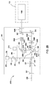
- 基板を熱処理する装置であって、
電磁エネルギーパルスを生成するように動作可能な電磁エネルギー源と、
パルスコンバイナ、パルスシェーパ、ホモジナイザおよび開孔部材を備える光学システムであって、開孔部材が中に埋め込まれた反射部分と電磁エネルギーが通って投影される透過性部材とを有し、反射部分の表面が電磁エネルギーの焦点面に位置決めされる、光学システムと、
前記光学システムに対して基板を移動させるように動作可能な基板支持体と、
前記光学システムの光路に沿って前記基板を視認するように動作可能であって結像誘導光学系と結像検出器を含む結像システムと
を備える装置。 - 前記パルスコンバイナは第1のパルスを偏光する第1の偏光子と、第2のパルスを偏光する第2の偏光子と、偏光面を有する合成光学系とを備え、前記第1のパルスおよび前記第2のパルスは前記偏光面の互いに反対側に誘導される、請求項1に記載の装置。
- 前記結像システムは、基板から反射された光を結像検出器に選択的に反射するサンプリング光学系をさらに備える、請求項1に記載の装置。
Applications Claiming Priority (7)
| Application Number | Priority Date | Filing Date | Title |
|---|---|---|---|
| US201161500727P | 2011-06-24 | 2011-06-24 | |
| US61/500,727 | 2011-06-24 | ||
| US13/194,775 US8569187B2 (en) | 2011-06-24 | 2011-07-29 | Thermal processing apparatus |
| US13/194,552 | 2011-07-29 | ||
| US13/194,775 | 2011-07-29 | ||
| US13/194,552 US20120325784A1 (en) | 2011-06-24 | 2011-07-29 | Novel thermal processing apparatus |
| PCT/US2012/043323 WO2012177743A2 (en) | 2011-06-24 | 2012-06-20 | Novel thermal processing apparatus |
Related Child Applications (1)
| Application Number | Title | Priority Date | Filing Date |
|---|---|---|---|
| JP2016164422A Division JP6290997B2 (ja) | 2011-06-24 | 2016-08-25 | 新規の熱処理装置 |
Publications (3)
| Publication Number | Publication Date |
|---|---|
| JP2014525141A JP2014525141A (ja) | 2014-09-25 |
| JP2014525141A5 JP2014525141A5 (ja) | 2015-08-06 |
| JP6096184B2 true JP6096184B2 (ja) | 2017-03-15 |
Family
ID=47360854
Family Applications (3)
| Application Number | Title | Priority Date | Filing Date |
|---|---|---|---|
| JP2014517117A Active JP6096184B2 (ja) | 2011-06-24 | 2012-06-20 | 新規の熱処理装置 |
| JP2016164422A Active JP6290997B2 (ja) | 2011-06-24 | 2016-08-25 | 新規の熱処理装置 |
| JP2017025629A Active JP6321237B2 (ja) | 2011-06-24 | 2017-02-15 | 新規の熱処理装置 |
Family Applications After (2)
| Application Number | Title | Priority Date | Filing Date |
|---|---|---|---|
| JP2016164422A Active JP6290997B2 (ja) | 2011-06-24 | 2016-08-25 | 新規の熱処理装置 |
| JP2017025629A Active JP6321237B2 (ja) | 2011-06-24 | 2017-02-15 | 新規の熱処理装置 |
Country Status (7)
| Country | Link |
|---|---|
| US (3) | US8569187B2 (ja) |
| EP (1) | EP2724364B1 (ja) |
| JP (3) | JP6096184B2 (ja) |
| KR (1) | KR101987398B1 (ja) |
| CN (2) | CN103597587B (ja) |
| TW (4) | TWI547978B (ja) |
| WO (1) | WO2012177743A2 (ja) |
Families Citing this family (32)
| Publication number | Priority date | Publication date | Assignee | Title |
|---|---|---|---|---|
| US9498845B2 (en) | 2007-11-08 | 2016-11-22 | Applied Materials, Inc. | Pulse train annealing method and apparatus |
| US8569187B2 (en) * | 2011-06-24 | 2013-10-29 | Applied Materials, Inc. | Thermal processing apparatus |
| FR2989388B1 (fr) * | 2012-04-17 | 2019-10-18 | Saint-Gobain Glass France | Procede d'obtention d'un substrat muni d'un revetement |
| JP2015521368A (ja) * | 2012-04-18 | 2015-07-27 | アプライド マテリアルズ インコーポレイテッドApplied Materials,Incorporated | アドバンスアニールプロセスにおいて粒子を低減させる装置および方法 |
| US9146337B2 (en) | 2013-03-11 | 2015-09-29 | Applied Materials, Inc. | Apparatus for speckle reduction, pulse stretching, and beam homogenization |
| US9390926B2 (en) * | 2013-03-11 | 2016-07-12 | Applied Materials, Inc. | Process sheet resistance uniformity improvement using multiple melt laser exposures |
| CN105643107B (zh) | 2013-03-12 | 2019-03-01 | 应用材料公司 | 在激光退火系统中用于控制边缘轮廓的定制光瞳光阑形状 |
| KR102163606B1 (ko) * | 2013-03-27 | 2020-10-08 | 고쿠리쓰다이가쿠호진 규슈다이가쿠 | 레이저 어닐링 장치 |
| CN105453231B (zh) * | 2013-08-08 | 2019-06-11 | 应用材料公司 | 用于使用耗尽光束形成亚微米特征结构的反应物的光子活化 |
| US9958709B2 (en) | 2013-08-16 | 2018-05-01 | Applied Materials, Inc. | Dynamic optical valve for mitigating non-uniform heating in laser processing |
| US11204506B2 (en) * | 2014-03-05 | 2021-12-21 | TeraDiode, Inc. | Polarization-adjusted and shape-adjusted beam operation for materials processing |
| US9889524B2 (en) * | 2014-03-05 | 2018-02-13 | TeraDiode, Inc. | Polarization-adjusted beam operation for materials processing |
| JP6430142B2 (ja) * | 2014-04-25 | 2018-11-28 | 浜松ホトニクス株式会社 | レーザ加工モニタ及びレーザ加工装置 |
| US10239155B1 (en) * | 2014-04-30 | 2019-03-26 | The Boeing Company | Multiple laser beam processing |
| CN106663629B (zh) * | 2014-07-21 | 2020-01-10 | 应用材料公司 | 扫描脉冲退火装置及方法 |
| US10095114B2 (en) | 2014-11-14 | 2018-10-09 | Applied Materials, Inc. | Process chamber for field guided exposure and method for implementing the process chamber |
| CN106158609B (zh) * | 2015-03-31 | 2019-07-23 | 上海微电子装备(集团)股份有限公司 | 一种激光退火装置及其退火方法 |
| US9864276B2 (en) | 2015-04-07 | 2018-01-09 | Applied Materials, Inc. | Laser annealing and electric field |
| US10843266B2 (en) | 2015-10-30 | 2020-11-24 | Seurat Technologies, Inc. | Chamber systems for additive manufacturing |
| JP6920316B2 (ja) * | 2016-09-06 | 2021-08-18 | ギガフォトン株式会社 | レーザ装置およびレーザアニール装置 |
| HUE064074T2 (hu) * | 2016-11-18 | 2024-02-28 | Ipg Photonics Corp | Összeállítás és eljárás anyagok lézeres feldolgozására |
| US10012544B2 (en) * | 2016-11-29 | 2018-07-03 | Cymer, Llc | Homogenization of light beam for spectral feature metrology |
| CN110214364A (zh) * | 2017-02-02 | 2019-09-06 | 三菱电机株式会社 | 热处理装置、热处理方法和半导体装置的制造方法 |
| JP7254444B2 (ja) * | 2018-02-13 | 2023-04-10 | 旭化成株式会社 | 金属配線の製造方法及び金属配線製造装置 |
| JP7048372B2 (ja) * | 2018-03-20 | 2022-04-05 | 株式会社Screenホールディングス | 熱処理装置および熱処理方法 |
| JP7328427B2 (ja) | 2018-03-28 | 2023-08-16 | 株式会社東京精密 | 板厚の測定装置及び板厚の測定方法 |
| WO2019199601A1 (en) * | 2018-04-12 | 2019-10-17 | Mattson Technology, Inc. | Low thermal budget annealing |
| JP2022518411A (ja) | 2019-01-18 | 2022-03-15 | アプライド マテリアルズ インコーポレイテッド | 電界誘導フォトレジストパターン形成工程のためのフィルム構造 |
| CN110767576B (zh) * | 2019-10-17 | 2022-10-21 | 上海华力集成电路制造有限公司 | 激光退火设备及激光退火工艺 |
| GB2593456B (en) * | 2020-03-18 | 2024-02-28 | Thermo Fisher Scient Ecublens Sarl | Double-pulse laser system |
| US11429026B2 (en) | 2020-03-20 | 2022-08-30 | Applied Materials, Inc. | Lithography process window enhancement for photoresist patterning |
| US11909091B2 (en) | 2020-05-19 | 2024-02-20 | Kymeta Corporation | Expansion compensation structure for an antenna |
Family Cites Families (43)
| Publication number | Priority date | Publication date | Assignee | Title |
|---|---|---|---|---|
| US4663513A (en) * | 1985-11-26 | 1987-05-05 | Spectra-Physics, Inc. | Method and apparatus for monitoring laser processes |
| KR950034479A (ko) | 1994-05-24 | 1995-12-28 | 오노 시게오 | 조명광학계 |
| JP3435247B2 (ja) * | 1995-02-28 | 2003-08-11 | 株式会社東芝 | レーザ光照射装置及びレーザ光照射方法 |
| US5975703A (en) * | 1996-09-30 | 1999-11-02 | Digital Optics International | Image projection system |
| JP4322373B2 (ja) * | 1999-11-15 | 2009-08-26 | 日本電気株式会社 | 膜体部改質装置及び膜体部改質方法 |
| US6366308B1 (en) * | 2000-02-16 | 2002-04-02 | Ultratech Stepper, Inc. | Laser thermal processing apparatus and method |
| US6639177B2 (en) | 2001-03-29 | 2003-10-28 | Gsi Lumonics Corporation | Method and system for processing one or more microstructures of a multi-material device |
| JP3903761B2 (ja) | 2001-10-10 | 2007-04-11 | 株式会社日立製作所 | レ−ザアニ−ル方法およびレ−ザアニ−ル装置 |
| JP2003124137A (ja) | 2001-10-10 | 2003-04-25 | Fujitsu Ltd | 半導体製造装置 |
| JP2004063924A (ja) | 2002-07-31 | 2004-02-26 | Mitsubishi Heavy Ind Ltd | レーザアニール方法及び装置 |
| US6747245B2 (en) | 2002-11-06 | 2004-06-08 | Ultratech Stepper, Inc. | Laser scanning apparatus and methods for thermal processing |
| SG137674A1 (en) * | 2003-04-24 | 2007-12-28 | Semiconductor Energy Lab | Beam homogenizer, laser irradiation apparatus, and method for manufacturing semiconductor device |
| JP4467571B2 (ja) * | 2003-09-19 | 2010-05-26 | アプライド マテリアルズ インコーポレイテッド | 無電解堆積のエンドポイントを検出するための装置および方法 |
| JP2005116729A (ja) | 2003-10-07 | 2005-04-28 | Sharp Corp | レーザ加工装置およびレーザ加工方法 |
| US7813406B1 (en) | 2003-10-15 | 2010-10-12 | The United States Of America As Represented By The Administrator Of The National Aeronautics And Space Administration | Temporal laser pulse manipulation using multiple optical ring-cavities |
| WO2005074002A2 (en) * | 2004-01-29 | 2005-08-11 | Applied Materials Israel, Ltd. | Focusing system and method for a charged particle imaging system |
| JP4610201B2 (ja) * | 2004-01-30 | 2011-01-12 | 住友重機械工業株式会社 | レーザ照射装置 |
| US8110775B2 (en) | 2004-06-18 | 2012-02-07 | Electro Scientific Industries, Inc. | Systems and methods for distinguishing reflections of multiple laser beams for calibration for semiconductor structure processing |
| US20090011614A1 (en) * | 2004-06-18 | 2009-01-08 | Electro Scientific Industries, Inc. | Reconfigurable semiconductor structure processing using multiple laser beam spots |
| US20060114948A1 (en) * | 2004-11-29 | 2006-06-01 | Lo Ho W | Workpiece processing system using a common imaged optical assembly to shape the spatial distributions of light energy of multiple laser beams |
| JP2006185933A (ja) * | 2004-12-24 | 2006-07-13 | Advanced Lcd Technologies Development Center Co Ltd | レーザアニール方法およびレーザアニール装置 |
| US7279721B2 (en) | 2005-04-13 | 2007-10-09 | Applied Materials, Inc. | Dual wavelength thermal flux laser anneal |
| JP2006344844A (ja) * | 2005-06-10 | 2006-12-21 | Sony Corp | レーザ処理装置 |
| JP2007059431A (ja) | 2005-08-22 | 2007-03-08 | Mitsubishi Electric Corp | 半導体装置の製造方法及びレーザ加工装置 |
| JP4956987B2 (ja) | 2005-12-16 | 2012-06-20 | 株式会社島津製作所 | レーザー結晶化装置及び結晶化方法 |
| US7569463B2 (en) | 2006-03-08 | 2009-08-04 | Applied Materials, Inc. | Method of thermal processing structures formed on a substrate |
| WO2007137995A2 (en) * | 2006-06-01 | 2007-12-06 | Universite De Liege | A thermal detector |
| JP5000944B2 (ja) * | 2006-08-02 | 2012-08-15 | 株式会社ディスコ | レーザー加工装置のアライメント方法 |
| JP4677392B2 (ja) | 2006-10-30 | 2011-04-27 | 住友重機械工業株式会社 | パルスレーザ熱処理装置とその制御方法 |
| US20090323739A1 (en) * | 2006-12-22 | 2009-12-31 | Uv Tech Systems | Laser optical system |
| US20080316748A1 (en) * | 2007-06-21 | 2008-12-25 | Carl Zeiss Laser Optics Gmbh | Illumination system |
| US8148663B2 (en) * | 2007-07-31 | 2012-04-03 | Applied Materials, Inc. | Apparatus and method of improving beam shaping and beam homogenization |
| US20090034072A1 (en) * | 2007-07-31 | 2009-02-05 | Dean Jennings | Method and apparatus for decorrelation of spatially and temporally coherent light |
| US8332922B2 (en) * | 2007-08-31 | 2012-12-11 | Microsoft Corporation | Transferable restricted security tokens |
| US20090120924A1 (en) * | 2007-11-08 | 2009-05-14 | Stephen Moffatt | Pulse train annealing method and apparatus |
| US8723073B2 (en) * | 2008-02-07 | 2014-05-13 | Cymer, Llc | Illumination apparatus and method for controlling energy of a laser source |
| US8674257B2 (en) * | 2008-02-11 | 2014-03-18 | Applied Materials, Inc. | Automatic focus and emissivity measurements for a substrate system |
| US8178818B2 (en) | 2008-03-31 | 2012-05-15 | Electro Scientific Industries, Inc. | Photonic milling using dynamic beam arrays |
| US7982160B2 (en) | 2008-03-31 | 2011-07-19 | Electro Scientific Industries, Inc. | Photonic clock stabilized laser comb processing |
| US7919348B2 (en) * | 2008-06-13 | 2011-04-05 | Aptina Imaging Corporation | Methods for protecting imaging elements of photoimagers during back side processing |
| CN102414787B (zh) * | 2009-09-02 | 2014-05-21 | Wi-A株式会社 | 激光反射掩模以及其制造方法 |
| TWI575630B (zh) * | 2011-06-10 | 2017-03-21 | 應用材料股份有限公司 | 脈衝循環器 |
| US8569187B2 (en) * | 2011-06-24 | 2013-10-29 | Applied Materials, Inc. | Thermal processing apparatus |
-
2011
- 2011-07-29 US US13/194,775 patent/US8569187B2/en active Active
- 2011-07-29 US US13/194,552 patent/US20120325784A1/en not_active Abandoned
-
2012
- 2012-06-07 TW TW101120494A patent/TWI547978B/zh active
- 2012-06-07 TW TW107145005A patent/TWI700736B/zh active
- 2012-06-07 TW TW106128051A patent/TWI654669B/zh active
- 2012-06-07 TW TW105115758A patent/TWI600063B/zh active
- 2012-06-20 WO PCT/US2012/043323 patent/WO2012177743A2/en unknown
- 2012-06-20 EP EP12802296.9A patent/EP2724364B1/en active Active
- 2012-06-20 KR KR1020147001261A patent/KR101987398B1/ko active IP Right Grant
- 2012-06-20 CN CN201280027949.XA patent/CN103597587B/zh active Active
- 2012-06-20 JP JP2014517117A patent/JP6096184B2/ja active Active
- 2012-06-20 CN CN201610565610.5A patent/CN106141424B/zh active Active
-
2014
- 2014-01-24 US US14/163,309 patent/US10181409B2/en active Active
-
2016
- 2016-08-25 JP JP2016164422A patent/JP6290997B2/ja active Active
-
2017
- 2017-02-15 JP JP2017025629A patent/JP6321237B2/ja active Active
Also Published As
| Publication number | Publication date |
|---|---|
| JP6321237B2 (ja) | 2018-05-09 |
| TWI654669B (zh) | 2019-03-21 |
| US10181409B2 (en) | 2019-01-15 |
| JP2017135390A (ja) | 2017-08-03 |
| JP6290997B2 (ja) | 2018-03-07 |
| EP2724364A4 (en) | 2015-09-30 |
| US20140138362A1 (en) | 2014-05-22 |
| CN103597587A (zh) | 2014-02-19 |
| US8569187B2 (en) | 2013-10-29 |
| CN106141424A (zh) | 2016-11-23 |
| TWI547978B (zh) | 2016-09-01 |
| JP2014525141A (ja) | 2014-09-25 |
| TW201926423A (zh) | 2019-07-01 |
| EP2724364B1 (en) | 2020-04-29 |
| WO2012177743A3 (en) | 2013-04-04 |
| TW201812868A (zh) | 2018-04-01 |
| TW201637079A (zh) | 2016-10-16 |
| WO2012177743A2 (en) | 2012-12-27 |
| TW201303977A (zh) | 2013-01-16 |
| EP2724364A2 (en) | 2014-04-30 |
| KR101987398B1 (ko) | 2019-06-10 |
| US20120329178A1 (en) | 2012-12-27 |
| US20120325784A1 (en) | 2012-12-27 |
| TWI700736B (zh) | 2020-08-01 |
| JP2017041637A (ja) | 2017-02-23 |
| CN103597587B (zh) | 2016-08-17 |
| CN106141424B (zh) | 2018-05-29 |
| KR20140039300A (ko) | 2014-04-01 |
| TWI600063B (zh) | 2017-09-21 |
Similar Documents
| Publication | Publication Date | Title |
|---|---|---|
| JP6321237B2 (ja) | 新規の熱処理装置 | |
| US9953851B2 (en) | Process sheet resistance uniformity improvement using multiple melt laser exposures | |
| JP2014525141A5 (ja) | ||
| KR100722723B1 (ko) | 열 처리를 위한 레이저 주사 장치 및 방법 | |
| TWI582466B (zh) | 用於改良同調光的能源的均勻性的裝置及用於產生均勻照明場的裝置 | |
| KR20150058445A (ko) | 펄스 폭 제어기 | |
| KR20140048188A (ko) | 펄스 써큘레이터 | |
| US20170011917A1 (en) | Atomic layer epitaxy for semiconductor gate stack layer for advanced channel devices | |
| US9146337B2 (en) | Apparatus for speckle reduction, pulse stretching, and beam homogenization |
Legal Events
| Date | Code | Title | Description |
|---|---|---|---|
| A521 | Request for written amendment filed |
Free format text: JAPANESE INTERMEDIATE CODE: A523 Effective date: 20150619 |
|
| A621 | Written request for application examination |
Free format text: JAPANESE INTERMEDIATE CODE: A621 Effective date: 20150619 |
|
| A977 | Report on retrieval |
Free format text: JAPANESE INTERMEDIATE CODE: A971007 Effective date: 20160523 |
|
| A131 | Notification of reasons for refusal |
Free format text: JAPANESE INTERMEDIATE CODE: A131 Effective date: 20160531 |
|
| A521 | Request for written amendment filed |
Free format text: JAPANESE INTERMEDIATE CODE: A523 Effective date: 20160825 |
|
| TRDD | Decision of grant or rejection written | ||
| A01 | Written decision to grant a patent or to grant a registration (utility model) |
Free format text: JAPANESE INTERMEDIATE CODE: A01 Effective date: 20170117 |
|
| A61 | First payment of annual fees (during grant procedure) |
Free format text: JAPANESE INTERMEDIATE CODE: A61 Effective date: 20170215 |
|
| R150 | Certificate of patent or registration of utility model |
Ref document number: 6096184 Country of ref document: JP Free format text: JAPANESE INTERMEDIATE CODE: R150 |
|
| R250 | Receipt of annual fees |
Free format text: JAPANESE INTERMEDIATE CODE: R250 |
|
| R250 | Receipt of annual fees |
Free format text: JAPANESE INTERMEDIATE CODE: R250 |
|
| R250 | Receipt of annual fees |
Free format text: JAPANESE INTERMEDIATE CODE: R250 |
|
| R250 | Receipt of annual fees |
Free format text: JAPANESE INTERMEDIATE CODE: R250 |
|
| R250 | Receipt of annual fees |
Free format text: JAPANESE INTERMEDIATE CODE: R250 |