JP5995416B2 - 撮像素子及び撮像装置 - Google Patents
撮像素子及び撮像装置 Download PDFInfo
- Publication number
- JP5995416B2 JP5995416B2 JP2011183076A JP2011183076A JP5995416B2 JP 5995416 B2 JP5995416 B2 JP 5995416B2 JP 2011183076 A JP2011183076 A JP 2011183076A JP 2011183076 A JP2011183076 A JP 2011183076A JP 5995416 B2 JP5995416 B2 JP 5995416B2
- Authority
- JP
- Japan
- Prior art keywords
- signal
- photoelectric conversion
- electrode
- microlens
- insulating layer
- Prior art date
- Legal status (The legal status is an assumption and is not a legal conclusion. Google has not performed a legal analysis and makes no representation as to the accuracy of the status listed.)
- Expired - Fee Related
Links
Images


Description
特許文献1,2のように分割画素を構成する際、各分割画素の間には、様々な画素構成要素が配置される可能性がある。例えば、感度向上のためにフォトダイオードの面積を大きくしたい場合、各分割画素毎にフローティングディフュージョン(以下、FD)や出力信号線を配置するのではなく、複数の分割画素で共有するFDなどを使用する構成が好ましい。この際、共有するFDは、各分割画素の中心に配置することが望ましい。このように、各分割画素間に、FDなどの画素構成要素を配置するために、各分割画素のフォトダイオード間には、感度を持たない分離領域が存在することになる。
Claims (6)
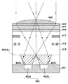
- マイクロレンズを共有し、且つ分離層にて複数の領域に分割された光電変換部と、前記マイクロレンズにて集光された光束を前記光電変換部に導くとともに前記分離層には導かない光導波路と、電極が配置され前記分離層を覆う絶縁層と、を有する撮像素子であって、
前記分離層は前記光電変換部で発生した電荷を転送するための転送電極を備え、
前記絶縁層は前記光導波路内の光を反射するための境界面を有し、
前記光導波路は、前記複数の領域に分割された光電変換部の各々の上面に積層され、
前記光導波路上に前記絶縁層が積層され、
前記絶縁層上に前記マイクロレンズが積層され、
光入射方向において、前記光導波路の各々の前記光電変換部側の面は、前記分離層に備わる前記転送電極を覆わずに前記光電変換部の光入射面を覆い、
光入射方向において、前記光導波路の各々の前記絶縁層と接する側の面は、平面であり、前記分離層と前記光電変換部の光入射面を覆っていることを特徴とする撮像素子。 - 前記光導波路は、前記マイクロレンズの結像位置の近傍に配置されることを特徴とする請求項1に記載の撮像素子。
- 前記光導波路は、前記マイクロレンズの結像位置より後方に配置されることを特徴とする請求項1又は2に記載の撮像素子。
- 前記光導波路の各々の前記絶縁層側の面は、その周縁部が前記マイクロレンズの光軸上で接しており、
前記マイクロレンズに入射した光束は、前記光導波路の各々の前記絶縁層側の面に集光し、
前記光導波路の各々に入射した光束は、前記複数の領域に分割された光電変換部の各々に到達することを特徴とする請求項1乃至3のいずれか1項に記載の撮像素子。 - 前記電極は、前記光電変換部から転送された電荷を選択的に出力する第1の電極、第2の電極及び第3の電極を含み、
前記絶縁層は、前記第1の電極と前記第2の電極の間、及び、前記第2の電極と前記第3の電極の間に配置されていることを特徴とする請求項1乃至4のいずれか1項に記載の撮像素子。 - 撮影レンズと、
前記撮影レンズを介した光束を受光する請求項1乃至5のいずれか1項に記載の撮像素子と、を備えることを特徴とする撮像装置。
Priority Applications (1)
| Application Number | Priority Date | Filing Date | Title |
|---|---|---|---|
| JP2011183076A JP5995416B2 (ja) | 2011-08-24 | 2011-08-24 | 撮像素子及び撮像装置 |
Applications Claiming Priority (1)
| Application Number | Priority Date | Filing Date | Title |
|---|---|---|---|
| JP2011183076A JP5995416B2 (ja) | 2011-08-24 | 2011-08-24 | 撮像素子及び撮像装置 |
Publications (3)
| Publication Number | Publication Date |
|---|---|
| JP2013045907A JP2013045907A (ja) | 2013-03-04 |
| JP2013045907A5 JP2013045907A5 (ja) | 2014-09-18 |
| JP5995416B2 true JP5995416B2 (ja) | 2016-09-21 |
Family
ID=48009577
Family Applications (1)
| Application Number | Title | Priority Date | Filing Date |
|---|---|---|---|
| JP2011183076A Expired - Fee Related JP5995416B2 (ja) | 2011-08-24 | 2011-08-24 | 撮像素子及び撮像装置 |
Country Status (1)
| Country | Link |
|---|---|
| JP (1) | JP5995416B2 (ja) |
Families Citing this family (9)
| Publication number | Priority date | Publication date | Assignee | Title |
|---|---|---|---|---|
| JP5813047B2 (ja) * | 2013-04-26 | 2015-11-17 | キヤノン株式会社 | 撮像装置、および、撮像システム。 |
| JP6338442B2 (ja) * | 2013-07-11 | 2018-06-06 | キヤノン株式会社 | 固体撮像素子、測距装置、および撮像装置 |
| JP6444066B2 (ja) * | 2014-06-02 | 2018-12-26 | キヤノン株式会社 | 光電変換装置および撮像システム |
| JP6425427B2 (ja) * | 2014-06-16 | 2018-11-21 | キヤノン株式会社 | 光電変換装置およびその製造方法、撮像システム |
| JP2016031993A (ja) * | 2014-07-28 | 2016-03-07 | キヤノン株式会社 | 固体撮像装置及びカメラ |
| JP2016058559A (ja) * | 2014-09-10 | 2016-04-21 | ソニー株式会社 | 固体撮像装置およびその駆動方法、並びに電子機器 |
| JP6595839B2 (ja) * | 2015-08-05 | 2019-10-23 | キヤノン株式会社 | 撮像素子およびその制御方法、ならびに撮像装置 |
| CN115037888A (zh) * | 2017-11-22 | 2022-09-09 | 索尼半导体解决方案公司 | 固态摄像元件和电子设备 |
| JP2024039120A (ja) * | 2022-09-09 | 2024-03-22 | ソニーセミコンダクタソリューションズ株式会社 | 光検出装置および電子機器 |
Family Cites Families (5)
| Publication number | Priority date | Publication date | Assignee | Title |
|---|---|---|---|---|
| JPH0590551A (ja) * | 1991-09-30 | 1993-04-09 | Toshiba Corp | 固体撮像装置 |
| JP2002076312A (ja) * | 2000-08-28 | 2002-03-15 | Fuji Film Microdevices Co Ltd | 固体撮像素子 |
| JP2008141014A (ja) * | 2006-12-01 | 2008-06-19 | Internatl Business Mach Corp <Ibm> | ピクセル・センサ構造、半導体構造の製造方法(ピクセル・センサ用の漏斗状光パイプ) |
| JP5422889B2 (ja) * | 2007-12-27 | 2014-02-19 | 株式会社ニコン | 固体撮像素子及びこれを用いた撮像装置 |
| US8792027B2 (en) * | 2010-01-06 | 2014-07-29 | Panasonic Corporation | Solid-state image pickup device, imaging device, and dispersing element |
-
2011
- 2011-08-24 JP JP2011183076A patent/JP5995416B2/ja not_active Expired - Fee Related
Also Published As
| Publication number | Publication date |
|---|---|
| JP2013045907A (ja) | 2013-03-04 |
Similar Documents
| Publication | Publication Date | Title |
|---|---|---|
| JP5995416B2 (ja) | 撮像素子及び撮像装置 | |
| JP6041495B2 (ja) | 撮像装置及び欠陥画素の判定方法 | |
| US10163971B2 (en) | Image sensor, image capturing apparatus, and forming method | |
| JP5045012B2 (ja) | 固体撮像素子及びこれを用いた撮像装置 | |
| JP4532800B2 (ja) | 撮像装置及びシステム | |
| US8089545B2 (en) | Solid-state image pickup device and control method thereof, and camera | |
| JP4448888B2 (ja) | 撮像装置及び撮像装置の信号処理方法 | |
| JP4839990B2 (ja) | 固体撮像素子及びこれを用いた撮像装置 | |
| US20060208292A1 (en) | Image pickup device and camera with expanded dynamic range | |
| WO2013172205A1 (ja) | 撮像装置および撮像方法、電子機器、並びにプログラム | |
| JP4579043B2 (ja) | 固体撮像素子及び撮像装置 | |
| JP2009049525A (ja) | 撮像装置及び信号処理方法 | |
| JP2006094263A (ja) | 撮像装置 | |
| JP2016103513A (ja) | 撮像素子および撮像装置 | |
| JP6733159B2 (ja) | 撮像素子、及び撮像装置 | |
| JP6358607B2 (ja) | 画像処理装置及び画像処理方法 | |
| JP6362099B2 (ja) | 撮像装置及びその制御方法、プログラム、記憶媒体 | |
| JP2009049524A (ja) | 撮像装置及び信号処理方法 | |
| JP4840992B2 (ja) | 光電変換装置及びその制御方法並びに撮像装置 | |
| JP2017208651A (ja) | 撮像装置 | |
| JP7247975B2 (ja) | 撮像素子及び撮像装置 | |
| JP7329136B2 (ja) | 撮像装置 | |
| JP5175783B2 (ja) | 撮像装置及び撮像装置の駆動方法 | |
| JP6451315B2 (ja) | 撮像装置 | |
| JP5961720B2 (ja) | 撮像装置 |
Legal Events
| Date | Code | Title | Description |
|---|---|---|---|
| A521 | Request for written amendment filed |
Free format text: JAPANESE INTERMEDIATE CODE: A523 Effective date: 20140731 |
|
| A621 | Written request for application examination |
Free format text: JAPANESE INTERMEDIATE CODE: A621 Effective date: 20140731 |
|
| A977 | Report on retrieval |
Free format text: JAPANESE INTERMEDIATE CODE: A971007 Effective date: 20150514 |
|
| A131 | Notification of reasons for refusal |
Free format text: JAPANESE INTERMEDIATE CODE: A131 Effective date: 20150515 |
|
| A521 | Request for written amendment filed |
Free format text: JAPANESE INTERMEDIATE CODE: A523 Effective date: 20150713 |
|
| A131 | Notification of reasons for refusal |
Free format text: JAPANESE INTERMEDIATE CODE: A131 Effective date: 20160226 |
|
| A521 | Request for written amendment filed |
Free format text: JAPANESE INTERMEDIATE CODE: A523 Effective date: 20160413 |
|
| TRDD | Decision of grant or rejection written | ||
| A01 | Written decision to grant a patent or to grant a registration (utility model) |
Free format text: JAPANESE INTERMEDIATE CODE: A01 Effective date: 20160725 |
|
| A61 | First payment of annual fees (during grant procedure) |
Free format text: JAPANESE INTERMEDIATE CODE: A61 Effective date: 20160823 |
|
| R151 | Written notification of patent or utility model registration |
Ref document number: 5995416 Country of ref document: JP Free format text: JAPANESE INTERMEDIATE CODE: R151 |
|
| LAPS | Cancellation because of no payment of annual fees |