JP5836624B2 - 表示装置 - Google Patents
表示装置 Download PDFInfo
- Publication number
- JP5836624B2 JP5836624B2 JP2011088148A JP2011088148A JP5836624B2 JP 5836624 B2 JP5836624 B2 JP 5836624B2 JP 2011088148 A JP2011088148 A JP 2011088148A JP 2011088148 A JP2011088148 A JP 2011088148A JP 5836624 B2 JP5836624 B2 JP 5836624B2
- Authority
- JP
- Japan
- Prior art keywords
- composite member
- display device
- substrate
- convex portion
- carbon fibers
- Prior art date
- Legal status (The legal status is an assumption and is not a legal conclusion. Google has not performed a legal analysis and makes no representation as to the accuracy of the status listed.)
- Active
Links
Images


Classifications
-
- H—ELECTRICITY
- H10—SEMICONDUCTOR DEVICES; ELECTRIC SOLID-STATE DEVICES NOT OTHERWISE PROVIDED FOR
- H10K—ORGANIC ELECTRIC SOLID-STATE DEVICES
- H10K59/00—Integrated devices, or assemblies of multiple devices, comprising at least one organic light-emitting element covered by group H10K50/00
- H10K59/80—Constructional details
- H10K59/87—Passivation; Containers; Encapsulations
- H10K59/871—Self-supporting sealing arrangements
- H10K59/872—Containers
-
- G—PHYSICS
- G09—EDUCATION; CRYPTOGRAPHY; DISPLAY; ADVERTISING; SEALS
- G09F—DISPLAYING; ADVERTISING; SIGNS; LABELS OR NAME-PLATES; SEALS
- G09F9/00—Indicating arrangements for variable information in which the information is built-up on a support by selection or combination of individual elements
- G09F9/30—Indicating arrangements for variable information in which the information is built-up on a support by selection or combination of individual elements in which the desired character or characters are formed by combining individual elements
- G09F9/33—Indicating arrangements for variable information in which the information is built-up on a support by selection or combination of individual elements in which the desired character or characters are formed by combining individual elements being semiconductor devices, e.g. diodes
-
- G—PHYSICS
- G09—EDUCATION; CRYPTOGRAPHY; DISPLAY; ADVERTISING; SEALS
- G09F—DISPLAYING; ADVERTISING; SIGNS; LABELS OR NAME-PLATES; SEALS
- G09F9/00—Indicating arrangements for variable information in which the information is built-up on a support by selection or combination of individual elements
- G09F9/30—Indicating arrangements for variable information in which the information is built-up on a support by selection or combination of individual elements in which the desired character or characters are formed by combining individual elements
- G09F9/35—Indicating arrangements for variable information in which the information is built-up on a support by selection or combination of individual elements in which the desired character or characters are formed by combining individual elements being liquid crystals
-
- H—ELECTRICITY
- H04—ELECTRIC COMMUNICATION TECHNIQUE
- H04N—PICTORIAL COMMUNICATION, e.g. TELEVISION
- H04N5/00—Details of television systems
- H04N5/64—Constructional details of receivers, e.g. cabinets or dust covers
-
- H—ELECTRICITY
- H10—SEMICONDUCTOR DEVICES; ELECTRIC SOLID-STATE DEVICES NOT OTHERWISE PROVIDED FOR
- H10K—ORGANIC ELECTRIC SOLID-STATE DEVICES
- H10K59/00—Integrated devices, or assemblies of multiple devices, comprising at least one organic light-emitting element covered by group H10K50/00
- H10K59/80—Constructional details
- H10K59/87—Passivation; Containers; Encapsulations
- H10K59/871—Self-supporting sealing arrangements
- H10K59/8721—Metallic sealing arrangements
-
- H—ELECTRICITY
- H10—SEMICONDUCTOR DEVICES; ELECTRIC SOLID-STATE DEVICES NOT OTHERWISE PROVIDED FOR
- H10K—ORGANIC ELECTRIC SOLID-STATE DEVICES
- H10K59/00—Integrated devices, or assemblies of multiple devices, comprising at least one organic light-emitting element covered by group H10K50/00
- H10K59/80—Constructional details
- H10K59/87—Passivation; Containers; Encapsulations
- H10K59/871—Self-supporting sealing arrangements
- H10K59/8722—Peripheral sealing arrangements, e.g. adhesives, sealants
Landscapes
- Engineering & Computer Science (AREA)
- Physics & Mathematics (AREA)
- General Physics & Mathematics (AREA)
- Theoretical Computer Science (AREA)
- Multimedia (AREA)
- Signal Processing (AREA)
- Chemical & Material Sciences (AREA)
- Crystallography & Structural Chemistry (AREA)
- Devices For Indicating Variable Information By Combining Individual Elements (AREA)
- Electroluminescent Light Sources (AREA)
- Cathode-Ray Tubes And Fluorescent Screens For Display (AREA)
- Liquid Crystal (AREA)
Description
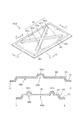
110 基板
120, 120a, 120b, 120c, 120d, 125, 587a, 587b, 587c, 587d, 687a, 687b, 687c, 687d, 687e リブ
125,160,260,360,460,560,660a,660b 突出部
130 表示部
140,240,340,440,540,640 延長部
150 シーリング部
170 金属膜
180A, 180B, 180C, 180D, 280A, 280B, 280C, 380A, 380B, 380C, 480A, 480B, 480C, 580A, 580B, 580C, 680A, 680B, 680B’, 680C 複合部材
180a 第1層
180b 第2層
180c 第3層
180d 第4層
181,181A,181B,181C,181D 樹脂マトリックス
182,182A,182B,182C,182D 炭素ファイバ
185,285,385 凸部
190A,190B,190C,190D 密封部
189, 289, 389, 489a, 489b, 589a, 589b, 689a, 689b 凹部
281,381,481,581,681 基底部
283,383,483,583,683 傾斜部
381a,485a 第1領域
381b,485b 第2領域
485,585,685 第1凸部
487,587,687 第2凸部
587e 中心部
Claims (25)
- 基板上に配された表示部と、
前記表示部と対向し、金属膜及び複合部材を具備し、前記複合部材が基底部と、前記基底部と段差を有する凸部とから構成された密封部と、
前記基板と前記密封部との間に、前記表示部と離隔されるように配され、前記基板と前記密封部とを接合するシーリング部と、を含み、
前記凸部は、上部面に突設された外部装置を表示装置に連結させる連結部材である突出部をさらに含むことを特徴とする表示装置。 - 前記凸部は、前記基板の反対側に、前記基底部から延設され、方形プレート状を有することを特徴とする請求項1に記載の表示装置。
- 前記凸部は、方形リング状を有することを特徴とする請求項1に記載の表示装置。
- 前記凸部は、
前記基板の反対側に、前記基底部から延設されて方形プレート状を有する第1凸部と、
前記第1凸部と段差を有して形成された楕円リング状の第2凸部と、を含むことを特徴とする請求項1に記載の表示装置。 - 前記凸部は、
前記基板の反対側に、前記基底部から延設されて方形プレート状を有する第1凸部と、
前記第1凸部と段差を有して形成されたX字状の第2凸部と、を含むことを特徴とする請求項1に記載の表示装置。 - 前記凸部は、
前記基板の反対側に、前記基底部から延設されて方形プレート状を有する第1凸部と、
前記第1凸部と段差を有して形成されたX字状の第2凸部と、を含むことを特徴とする請求項1に記載の表示装置。 - 前記凸部は、
前記基板の反対側に、前記基底部から延設されて方形プレート状を有する第1凸部と、
前記第1凸部と段差を有して形成されたストリップ状の第2凸部と、を含むことを特徴とする請求項1に記載の表示装置。 - 前記複合部材は、前記基板のエッジを取り囲むように、前記密封部のエッジから延びた延長部をさらに含むことを特徴とする請求項1に記載の表示装置。
- 前記複合部材は、樹脂マトリックス及び複数の炭素ファイバを含み、前記金属膜は、前記複合部材より前記基板にさらに近く配されることを特徴とする請求項1に記載の表示装置。
- 前記複数の炭素ファイバは、一方向に配された複数の炭素ファイバと、前記一方向と交差する方向に配された複数の炭素ファイバと、を具備することを特徴とする請求項9に記載の表示装置。
- 前記複数の炭素ファイバは、横方向及び縦方向に配されて織り上げられることを特徴とする請求項9に記載の表示装置。
- 前記炭素ファイバの熱膨張率は、前記基板の熱膨張率より小さいことを特徴とする請求項9に記載の表示装置。
- 前記複合部材は、複数の層に形成され、前記複数の層は、それぞれ樹脂マトリックス及び複数の炭素ファイバを含むことを特徴とする請求項1に記載の表示装置。
- 前記複数の層のうち少なくとも1層に配された炭素ファイバは、第1方向に配列され、前記複数の層のうち少なくとも他の1層に配された炭素ファイバは、第2方向に配列され、前記第1方向と前記第2方向は、交差することを特徴とする請求項13に記載の表示装置。
- 基板上に配された表示部と、
前記表示部と対向し、金属膜及び複合部材を具備し、前記複合部材の上部面に少なくとも1つのリブを具備する密封部と、
前記基板と前記密封部との間に、前記表示部と離隔されるように配され、前記基板と前記密封部とを接合するシーリング部と、を含み、
前記複合部材は、上部面に突設された外部装置を表示装置に連結させる連結部材である突出部をさらに含むことを特徴とする表示装置。 - 前記リブは、前記複合部材の長辺側に形成されたことを特徴とする請求項15に記載の表示装置。
- 前記複合部材は、前記基板のエッジを取り囲むように、前記密封部のエッジから延びた延長部をさらに含むことを特徴とする請求項15に記載の表示装置。
- 前記複合部材は、樹脂マトリックス及び複数の炭素ファイバを含み、前記金属膜は、前記複合部材より前記基板にさらに近く配されることを特徴とする請求項15に記載の表示装置。
- 前記複数の炭素ファイバは、一方向に配された複数の炭素ファイバと、前記一方向と交差する方向に配された複数の炭素ファイバと、を具備することを特徴とする請求項18に記載の表示装置。
- 前記複数の炭素ファイバは、横方向及び縦方向に配されて織り上げられることを特徴とする請求項18に記載の表示装置。
- 前記炭素ファイバの熱膨張率は、前記基板の熱膨張率より小さいことを特徴とする請求項18に記載の表示装置。
- 前記複合部材は、複数の層に形成され、前記複数の層は、それぞれ樹脂マトリックス及び複数の炭素ファイバを含むことを特徴とする請求項15に記載の表示装置。
- 前記複数の層のうち少なくとも1層に配された炭素ファイバは、第1方向に配列され、前記複数の層のうち少なくとも他の1層に配された炭素ファイバは、第2方向に配列され、前記第1方向と前記第2方向は、交差することを特徴とする請求項22に記載の表示装置。
- 前記第1方向と前記第2方向は、互いに直交することを特徴とする請求項23に記載の表示装置。
- 前記シーリング部は、エポキシ樹脂を含むことを特徴とする請求項15に記載の表示装置。
Applications Claiming Priority (2)
| Application Number | Priority Date | Filing Date | Title |
|---|---|---|---|
| KR10-2010-0051974 | 2010-06-01 | ||
| KR1020100051974A KR101798487B1 (ko) | 2010-06-01 | 2010-06-01 | 표시 장치 |
Publications (2)
| Publication Number | Publication Date |
|---|---|
| JP2011253177A JP2011253177A (ja) | 2011-12-15 |
| JP5836624B2 true JP5836624B2 (ja) | 2015-12-24 |
Family
ID=44118058
Family Applications (1)
| Application Number | Title | Priority Date | Filing Date |
|---|---|---|---|
| JP2011088148A Active JP5836624B2 (ja) | 2010-06-01 | 2011-04-12 | 表示装置 |
Country Status (5)
| Country | Link |
|---|---|
| US (1) | US8487533B2 (ja) |
| EP (1) | EP2393077A3 (ja) |
| JP (1) | JP5836624B2 (ja) |
| KR (1) | KR101798487B1 (ja) |
| CN (1) | CN102270748B (ja) |
Families Citing this family (4)
| Publication number | Priority date | Publication date | Assignee | Title |
|---|---|---|---|---|
| US9188323B2 (en) * | 2010-10-20 | 2015-11-17 | Semiconductor Energy Laboratory Co., Ltd. | Lighting device |
| CN106920888A (zh) * | 2015-12-24 | 2017-07-04 | 群创光电股份有限公司 | 发光装置及其制作方法 |
| CN109309171B (zh) * | 2018-09-29 | 2020-07-07 | 广州国显科技有限公司 | 有机电致发光器件及其制备方法、柔性显示装置 |
| KR20230036625A (ko) * | 2021-09-07 | 2023-03-15 | 삼성디스플레이 주식회사 | 표시 장치 |
Family Cites Families (35)
| Publication number | Priority date | Publication date | Assignee | Title |
|---|---|---|---|---|
| JPH06325868A (ja) * | 1993-03-15 | 1994-11-25 | Fuji Electric Co Ltd | 薄膜エレクトロルミネセンスパネル |
| JPH07169567A (ja) * | 1993-12-16 | 1995-07-04 | Idemitsu Kosan Co Ltd | 有機el素子 |
| JP2001118674A (ja) * | 1999-10-19 | 2001-04-27 | Auto Network Gijutsu Kenkyusho:Kk | 有機el表示装置 |
| JP2001290434A (ja) * | 2000-04-04 | 2001-10-19 | Nec Corp | 表示装置 |
| KR20030044665A (ko) | 2001-11-30 | 2003-06-09 | 오리온전기 주식회사 | 유기 el 패널용 봉지 커버 |
| CA2472965A1 (en) | 2002-01-25 | 2003-08-07 | Sumitomo Bakelite Co., Ltd | Transparent composite composition |
| JP2003229249A (ja) * | 2002-02-06 | 2003-08-15 | Canon Electronics Inc | 有機エレクトロルミネッセンスパネル |
| KR20030083528A (ko) * | 2002-04-23 | 2003-10-30 | 주식회사 대한전광 | 수직전기공급선을 구비한 유기전계발광소자 모듈 |
| TW589915B (en) * | 2002-05-24 | 2004-06-01 | Sanyo Electric Co | Electroluminescence display device |
| JP2004014267A (ja) | 2002-06-06 | 2004-01-15 | Nippon Sheet Glass Co Ltd | El素子用封止板、及び該封止板多面取り用マザーガラス基板 |
| US6998776B2 (en) | 2003-04-16 | 2006-02-14 | Corning Incorporated | Glass package that is hermetically sealed with a frit and method of fabrication |
| KR100669369B1 (ko) * | 2003-10-16 | 2007-01-15 | 삼성에스디아이 주식회사 | 플라즈마 표시장치 |
| JP2005317942A (ja) * | 2004-03-29 | 2005-11-10 | Toray Ind Inc | 電気・電子機器 |
| KR100570997B1 (ko) * | 2004-06-29 | 2006-04-13 | 삼성에스디아이 주식회사 | 평판 표시 장치 |
| JP2006085920A (ja) * | 2004-09-14 | 2006-03-30 | Nippon Steel Corp | 有機el背面キャップ |
| KR101227132B1 (ko) * | 2004-11-05 | 2013-01-28 | 엘지디스플레이 주식회사 | 유기 전계발광표시소자 및 그 제조방법 |
| JP2006185643A (ja) * | 2004-12-27 | 2006-07-13 | Optrex Corp | 有機elパネル |
| US7167365B2 (en) * | 2005-01-17 | 2007-01-23 | Chunghwa Picture Tubes, Ltd. | Back plate structure and plasma display apparatus |
| US20070020451A1 (en) * | 2005-07-20 | 2007-01-25 | 3M Innovative Properties Company | Moisture barrier coatings |
| JP2007073405A (ja) * | 2005-09-08 | 2007-03-22 | Konica Minolta Holdings Inc | 有機エレクトロルミネッセンス素子及びそれを用いた表示装置 |
| TWI428241B (zh) | 2005-10-26 | 2014-03-01 | 住友化學股份有限公司 | 經浸漬樹脂之底板及其製造方法 |
| US7537504B2 (en) | 2005-12-06 | 2009-05-26 | Corning Incorporated | Method of encapsulating a display element with frit wall and laser beam |
| JP4837471B2 (ja) * | 2006-02-20 | 2011-12-14 | 三星モバイルディスプレイ株式會社 | 有機電界発光表示装置及びその製造方法 |
| KR20070121974A (ko) | 2006-06-23 | 2007-12-28 | 엘지.필립스 엘시디 주식회사 | 유기 발광 표시 장치 및 그의 제조방법 |
| KR100747367B1 (ko) * | 2006-07-12 | 2007-08-07 | 엘지전자 주식회사 | 전계 발광 소자 |
| WO2008057045A1 (en) * | 2006-11-06 | 2008-05-15 | Agency For Science, Technology And Research | Nanoparticulate encapsulation barrier stack |
| KR100847003B1 (ko) | 2006-11-21 | 2008-07-17 | 대덕전자 주식회사 | 인쇄 회로 기판을 위한 탄소 섬유 보강재 |
| JP4867743B2 (ja) * | 2007-03-27 | 2012-02-01 | パナソニック電工株式会社 | 有機elモジュール |
| KR101458899B1 (ko) | 2007-03-28 | 2014-11-10 | 삼성디스플레이 주식회사 | 표시 장치 및 그 제조 방법 |
| EP2001047A1 (en) * | 2007-06-07 | 2008-12-10 | Semiconductor Energy Laboratory Co, Ltd. | Semiconductor device |
| CN201178100Y (zh) * | 2007-10-16 | 2009-01-07 | 西安海晶光电科技有限公司 | 带有机太阳能电池的有机电致发光显示屏 |
| KR101925772B1 (ko) * | 2008-07-10 | 2018-12-06 | 가부시키가이샤 한도오따이 에네루기 켄큐쇼 | 발광 장치 및 전자 기기 |
| KR20110114325A (ko) * | 2010-04-13 | 2011-10-19 | 삼성모바일디스플레이주식회사 | 표시 장치 |
| KR101808730B1 (ko) * | 2010-10-22 | 2017-12-14 | 삼성디스플레이 주식회사 | 유기 발광 표시 장치 |
| KR101804554B1 (ko) * | 2010-11-01 | 2017-12-05 | 삼성디스플레이 주식회사 | 표시 장치 및 유기 발광 표시 장치 |
-
2010
- 2010-06-01 KR KR1020100051974A patent/KR101798487B1/ko active Active
-
2011
- 2011-01-11 US US13/004,527 patent/US8487533B2/en active Active
- 2011-04-08 CN CN201110090163.XA patent/CN102270748B/zh active Active
- 2011-04-12 JP JP2011088148A patent/JP5836624B2/ja active Active
- 2011-05-31 EP EP11168213.4A patent/EP2393077A3/en not_active Withdrawn
Also Published As
| Publication number | Publication date |
|---|---|
| CN102270748B (zh) | 2016-12-07 |
| US8487533B2 (en) | 2013-07-16 |
| KR20110132133A (ko) | 2011-12-07 |
| EP2393077A2 (en) | 2011-12-07 |
| JP2011253177A (ja) | 2011-12-15 |
| US20110289809A1 (en) | 2011-12-01 |
| CN102270748A (zh) | 2011-12-07 |
| KR101798487B1 (ko) | 2017-11-17 |
| EP2393077A3 (en) | 2015-07-29 |
Similar Documents
| Publication | Publication Date | Title |
|---|---|---|
| US12488710B2 (en) | Display device and manufacturing method of display device | |
| JP6694928B2 (ja) | フレキシブルディスプレイ装置 | |
| US10269280B2 (en) | Display device and method of manufacturing the same | |
| KR102554240B1 (ko) | 표시 장치 및 표시 장치의 제조 방법 | |
| JP5836624B2 (ja) | 表示装置 | |
| US9406902B2 (en) | Flexible display panel having folding areas and non-folding areas | |
| US8093512B2 (en) | Package of environmentally sensitive electronic device and fabricating method thereof | |
| US10582615B2 (en) | Printed wiring board, printed circuit board, and electronic device | |
| KR102710098B1 (ko) | 엘이디 디스플레이 모듈 조립체 | |
| CN113555408B (zh) | 显示装置、显示模组及其制作方法 | |
| JP2017112108A (ja) | 有機発光表示装置 | |
| US11034128B2 (en) | Protection tape for printed circuit board and display device including the same | |
| US20140139985A1 (en) | Environmental sensitive electronic device package | |
| KR20210044486A (ko) | 플렉서블 표시 장치 및 이의 제조방법 | |
| KR20190006140A (ko) | 보호 필름, 이를 포함하는 윈도우 및 표시 장치의 제조 방법 | |
| US12443238B2 (en) | Display assembly and electronic device | |
| KR102576516B1 (ko) | 표시장치 | |
| US10860057B2 (en) | Display panel and display apparatus thereof | |
| CN111952337B (zh) | 显示模块、显示设备和制造显示设备的方法 | |
| US11240933B2 (en) | Heat radiation sheet | |
| KR102622369B1 (ko) | 연성인쇄회로필름 및 이를 포함하는 표시장치 | |
| KR101521713B1 (ko) | 표시장치 | |
| TWI531473B (zh) | 環境敏感電子元件封裝體及其製作方法 | |
| KR20130081924A (ko) | 유기 발광 표시 장치 및 그 제조 방법 | |
| US20240053806A1 (en) | Display device manufacturing apparatus and display device manufacturing method |
Legal Events
| Date | Code | Title | Description |
|---|---|---|---|
| A711 | Notification of change in applicant |
Free format text: JAPANESE INTERMEDIATE CODE: A712 Effective date: 20120921 |
|
| A621 | Written request for application examination |
Free format text: JAPANESE INTERMEDIATE CODE: A621 Effective date: 20140306 |
|
| A977 | Report on retrieval |
Free format text: JAPANESE INTERMEDIATE CODE: A971007 Effective date: 20150225 |
|
| A131 | Notification of reasons for refusal |
Free format text: JAPANESE INTERMEDIATE CODE: A131 Effective date: 20150303 |
|
| A521 | Request for written amendment filed |
Free format text: JAPANESE INTERMEDIATE CODE: A523 Effective date: 20150521 |
|
| TRDD | Decision of grant or rejection written | ||
| A01 | Written decision to grant a patent or to grant a registration (utility model) |
Free format text: JAPANESE INTERMEDIATE CODE: A01 Effective date: 20151006 |
|
| A61 | First payment of annual fees (during grant procedure) |
Free format text: JAPANESE INTERMEDIATE CODE: A61 Effective date: 20151104 |
|
| R150 | Certificate of patent or registration of utility model |
Ref document number: 5836624 Country of ref document: JP Free format text: JAPANESE INTERMEDIATE CODE: R150 |
|
| R250 | Receipt of annual fees |
Free format text: JAPANESE INTERMEDIATE CODE: R250 |
|
| R250 | Receipt of annual fees |
Free format text: JAPANESE INTERMEDIATE CODE: R250 |
|
| R250 | Receipt of annual fees |
Free format text: JAPANESE INTERMEDIATE CODE: R250 |
|
| R250 | Receipt of annual fees |
Free format text: JAPANESE INTERMEDIATE CODE: R250 |
|
| R250 | Receipt of annual fees |
Free format text: JAPANESE INTERMEDIATE CODE: R250 |
|
| R250 | Receipt of annual fees |
Free format text: JAPANESE INTERMEDIATE CODE: R250 |
|
| R250 | Receipt of annual fees |
Free format text: JAPANESE INTERMEDIATE CODE: R250 |
|
| R250 | Receipt of annual fees |
Free format text: JAPANESE INTERMEDIATE CODE: R250 |