JP5825742B2 - Semiconductor device - Google Patents
Semiconductor device Download PDFInfo
- Publication number
- JP5825742B2 JP5825742B2 JP2011135205A JP2011135205A JP5825742B2 JP 5825742 B2 JP5825742 B2 JP 5825742B2 JP 2011135205 A JP2011135205 A JP 2011135205A JP 2011135205 A JP2011135205 A JP 2011135205A JP 5825742 B2 JP5825742 B2 JP 5825742B2
- Authority
- JP
- Japan
- Prior art keywords
- transistor
- memory cell
- semiconductor device
- insulating layer
- potential
- Prior art date
- Legal status (The legal status is an assumption and is not a legal conclusion. Google has not performed a legal analysis and makes no representation as to the accuracy of the status listed.)
- Expired - Fee Related
Links
Images


Classifications
-
- G—PHYSICS
- G11—INFORMATION STORAGE
- G11C—STATIC STORES
- G11C11/00—Digital stores characterised by the use of particular electric or magnetic storage elements; Storage elements therefor
- G11C11/21—Digital stores characterised by the use of particular electric or magnetic storage elements; Storage elements therefor using electric elements
- G11C11/34—Digital stores characterised by the use of particular electric or magnetic storage elements; Storage elements therefor using electric elements using semiconductor devices
- G11C11/40—Digital stores characterised by the use of particular electric or magnetic storage elements; Storage elements therefor using electric elements using semiconductor devices using transistors
- G11C11/401—Digital stores characterised by the use of particular electric or magnetic storage elements; Storage elements therefor using electric elements using semiconductor devices using transistors forming cells needing refreshing or charge regeneration, i.e. dynamic cells
- G11C11/403—Digital stores characterised by the use of particular electric or magnetic storage elements; Storage elements therefor using electric elements using semiconductor devices using transistors forming cells needing refreshing or charge regeneration, i.e. dynamic cells with charge regeneration common to a multiplicity of memory cells, i.e. external refresh
-
- G—PHYSICS
- G11—INFORMATION STORAGE
- G11C—STATIC STORES
- G11C16/00—Erasable programmable read-only memories
- G11C16/02—Erasable programmable read-only memories electrically programmable
- G11C16/04—Erasable programmable read-only memories electrically programmable using variable threshold transistors, e.g. FAMOS
- G11C16/0408—Erasable programmable read-only memories electrically programmable using variable threshold transistors, e.g. FAMOS comprising cells containing floating gate transistors
- G11C16/0433—Erasable programmable read-only memories electrically programmable using variable threshold transistors, e.g. FAMOS comprising cells containing floating gate transistors comprising cells containing a single floating gate transistor and one or more separate select transistors
Landscapes
- Engineering & Computer Science (AREA)
- Microelectronics & Electronic Packaging (AREA)
- Computer Hardware Design (AREA)
- Semiconductor Memories (AREA)
- Thin Film Transistor (AREA)
- Non-Volatile Memory (AREA)
- Dram (AREA)
Description
開示する発明は、半導体素子を利用した半導体装置およびその作製方法に関するものである。 The disclosed invention relates to a semiconductor device using a semiconductor element and a manufacturing method thereof.
半導体素子を利用した記憶装置は、電力の供給がなくなると記憶内容が失われる揮発性のものと、電力の供給がなくなっても記憶内容は保持される不揮発性のものとに大別される。 Storage devices using semiconductor elements are roughly classified into a volatile type in which stored contents are lost when power is not supplied and a non-volatile type in which stored contents are retained even when power is supplied.
揮発性記憶装置の代表的な例としては、DRAM(Dynamic Random Access Memory)がある。DRAMは、記憶素子を構成するトランジスタを選択してキャパシタに電荷を蓄積することで、情報を記憶する。 A typical example of the volatile storage device is a DRAM (Dynamic Random Access Memory). A DRAM stores information by selecting a transistor constituting a memory element and accumulating electric charge in a capacitor.
上述の原理から、DRAMでは、情報を読み出すとキャパシタの電荷は失われるため、情報の読み出しの度に、再度の書き込み動作が必要となる。また、記憶素子を構成するトランジスタにおいてはオフ状態でのソースとドレイン間のリーク電流(オフ電流)等によって、トランジスタが選択されていない状況でも電荷が流出、または流入するため、データの保持期間が短い。このため、所定の周期で再度の書き込み動作(リフレッシュ動作)が必要であり、消費電力を十分に低減することは困難である。また、電力の供給がなくなると記憶内容が失われるため、長期間の記憶の保持には、磁性材料や光学材料を利用した別の記憶装置が必要となる。 Based on the above-described principle, in the DRAM, when information is read, the charge of the capacitor is lost. Therefore, every time information is read, a write operation is required again. In addition, in a transistor included in the memory element, electric charge flows out or flows in even in a state where the transistor is not selected due to a leakage current (off-state current) between the source and the drain in an off state. short. For this reason, a re-writing operation (refresh operation) is necessary at a predetermined cycle, and it is difficult to sufficiently reduce power consumption. Further, since the stored contents are lost when the power supply is stopped, another storage device using a magnetic material or an optical material is required to maintain the storage for a long time.
揮発性記憶装置の別の例としてはSRAM(Static Random Access Memory)がある。SRAMは、フリップフロップなどの回路を用いて記憶内容を保持するため、リフレッシュ動作が不要であり、この点においてはDRAMより有利である。しかし、フリップフロップなどの回路を用いているため、記憶容量あたりの単価が高くなるという問題がある。また、電力の供給がなくなると記憶内容が失われるという点については、DRAMと変わるところはない。 Another example of a volatile storage device is SRAM (Static Random Access Memory). An SRAM uses a circuit such as a flip-flop to hold stored contents, and therefore does not require a refresh operation. In this respect, the SRAM is more advantageous than a DRAM. However, since a circuit such as a flip-flop is used, there is a problem that the unit price per storage capacity increases. Further, there is no difference from DRAM in that the stored contents are lost when power supply is lost.
不揮発性記憶装置の代表例としては、フラッシュメモリがある。フラッシュメモリは、トランジスタのゲート電極とチャネル形成領域との間にフローティングゲートを有し、当該フローティングゲートに電荷を保持させることで記憶を行うため、データの保持期間は極めて長く(半永久的)、揮発性記憶装置で必要なリフレッシュ動作が不要であるという利点を有している(例えば、特許文献1参照)。 A typical example of the nonvolatile memory device is a flash memory. A flash memory has a floating gate between a gate electrode of a transistor and a channel formation region, and stores data by holding electric charge in the floating gate. Therefore, a data holding period is extremely long (semi-permanent) and volatile This has the advantage that the refresh operation necessary for the volatile memory device is not required (see, for example, Patent Document 1).
しかし、書き込みの際に生じるトンネル電流によって記憶素子を構成するゲート絶縁層が劣化するため、所定回数の書き込みによって記憶素子が機能しなくなるという問題が生じる。この問題の影響を緩和するために、例えば、各記憶素子の書き込み回数を均一化する手法が採られるが、これを実現するためには、複雑な周辺回路が必要になってしまう。そして、このような手法を採用しても、根本的な寿命の問題が解消するわけではない。つまり、フラッシュメモリは、情報の書き換え頻度が高い用途には不向きである。 However, the gate insulating layer included in the memory element is deteriorated by a tunnel current generated at the time of writing, which causes a problem that the memory element does not function after a predetermined number of writings. In order to alleviate the influence of this problem, for example, a method of making the number of writings of each storage element uniform is adopted, but in order to realize this, a complicated peripheral circuit is required. And even if such a method is adopted, the fundamental problem of lifetime is not solved. That is, the flash memory is not suitable for applications where the information rewriting frequency is high.
また、フローティングゲートに電荷を保持させるため、または、その電荷を除去するためには、高い電圧が必要であり、また、そのための回路も必要である。さらに、電荷の保持、または除去のためには比較的長い時間を要し、書き込み、消去の高速化が容易ではないという問題もある。 Further, in order to hold the charge in the floating gate or to remove the charge, a high voltage is required, and a circuit therefor is also necessary. Furthermore, there is a problem that it takes a relatively long time to hold or remove charges, and it is not easy to speed up writing and erasing.
上述の問題に鑑み、開示する発明の一態様では、電力が供給されない状況でも記憶内容の保持が可能で、かつ、書き込み回数にも制限が無い、新たな構造の半導体装置を提供することを目的の一とする。 In view of the above problems, an object of one embodiment of the disclosed invention is to provide a semiconductor device with a new structure that can retain stored data even when power is not supplied and has no limit on the number of times of writing. One of them.
開示する発明の一態様では、オフ電流が十分に小さいトランジスタを用いて情報を保持する半導体装置であって、当該半導体装置の情報の保持期間において、当該トランジスタのソース端子(またはドレイン端子)にはゲート端子より高い電位が与えられた状態となる半導体装置である。より具体的には、例えば、次のような構成を採用することができる。 In one embodiment of the disclosed invention, a semiconductor device holds information using a transistor with a sufficiently low off-state current, and the source terminal (or the drain terminal) of the transistor is included in the information holding period of the semiconductor device. This is a semiconductor device in which a higher potential is applied than the gate terminal. More specifically, for example, the following configuration can be adopted.
開示する発明の一態様は、ソース線と、ビット線と、ソース線とビット線との間に直列に接続された第1乃至第m(mは自然数)のメモリセルと、を有し、第1乃至第mのメモリセルはそれぞれ、第1のゲート端子、第1のソース端子、および第1のドレイン端子を有する第1のトランジスタと、第2のゲート端子、第2のソース端子、および第2のドレイン端子を有する第2のトランジスタと、容量素子と、を有し、第k(kは、1以上m以下を満たす自然数)のメモリセルの第2のソース端子は隣接するメモリセルの第2のドレイン端子と接続され、または第kのメモリセルの第2のドレイン端子は隣接するメモリセルの第2のソース端子と接続され、第kのメモリセルの第1のゲート端子と、第kのメモリセルの第2のソース端子(またはドレイン端子)と、第kのメモリセルの容量素子の端子の一方と、は電気的に接続されて第kのメモリセルのノードを構成し、第2のゲート端子に第2のトランジスタがオフ状態となる電位が与えられる情報の保持期間において、第kのメモリセルのノードは第kのメモリセルの第2のゲート端子より高い電位が与えられた状態となる半導体装置である。 One embodiment of the disclosed invention includes a source line, a bit line, and first to m-th (m is a natural number) memory cells connected in series between the source line and the bit line. Each of the first to mth memory cells includes a first transistor having a first gate terminal, a first source terminal, and a first drain terminal, a second gate terminal, a second source terminal, and a first transistor. A second transistor having a second drain terminal and a capacitor, and a second source terminal of a k-th (k is a natural number satisfying 1 to m) memory cell is a second memory terminal of an adjacent memory cell. The second drain terminal of the kth memory cell is connected to the second source terminal of the adjacent memory cell, the first gate terminal of the kth memory cell, and the kth memory cell. Memory cell second source terminal (M Is a drain terminal) and one of the capacitors of the kth memory cell is electrically connected to form a node of the kth memory cell, and the second transistor is turned off at the second gate terminal. In the retention period of information to which a potential to be turned on is applied, the node of the kth memory cell is a semiconductor device to which a higher potential is applied than the second gate terminal of the kth memory cell.
ここで、第1のトランジスタと第2のトランジスタは、互いに異なる半導体材料を主成分とする半導体領域を含む場合がある。また、第2のトランジスタは、金属酸化物を主成分とする半導体領域を含む場合がある。なお、以下では、「金属酸化物を主成分とする半導体」を、「酸化物半導体」と記す場合がある。 Here, the first transistor and the second transistor may include semiconductor regions containing different semiconductor materials as main components. The second transistor may include a semiconductor region containing a metal oxide as a main component. Hereinafter, the “semiconductor containing a metal oxide as a main component” may be referred to as an “oxide semiconductor”.
また、上記の情報の保持期間において、第kのメモリセルに隣接するメモリセルのノードは第kのメモリセルに隣接するメモリセルの第2のゲート端子より高い電位が与えられた状態となる場合がある。また、情報の保持期間において、第kのメモリセルの第2のゲート端子は接地電位が与えられた状態となる場合がある。また、情報の保持期間において、第kのメモリセルのノードは正の電位が与えられた状態となる場合がある。また、情報の保持期間において、第kのメモリセルの第2のゲート端子および第kのメモリセルのノードは、第kのメモリセルの第2のトランジスタを流れる電流が1zA以下となる電位が与えられた状態の場合がある。 In the above information holding period, the node of the memory cell adjacent to the kth memory cell is in a state where a higher potential is applied to the second gate terminal of the memory cell adjacent to the kth memory cell. There is. In addition, in the information retention period, the second gate terminal of the kth memory cell may be in a state where a ground potential is applied. In addition, in the information retention period, the node of the kth memory cell may be in a state where a positive potential is applied. In the information retention period, the second gate terminal of the kth memory cell and the node of the kth memory cell are given a potential at which the current flowing through the second transistor of the kth memory cell is 1 zA or less. May be in a state of being
また、上記構成において、第1のメモリセル、または第mのメモリセルをダミーセルとして用いる場合がある。また、第1のメモリセル、または第mのメモリセルが有する容量素子の容量値は、第2乃至第m−1のメモリセルのいずれかが有する容量素子の容量値より大きい場合がある。また、第1のメモリセル、または第mのメモリセルが有する第2のトランジスタのチャネル長は、第2乃至第m−1のメモリセルのいずれかが有する第2のトランジスタのチャネル長より大きい場合がある。 In the above structure, the first memory cell or the mth memory cell may be used as a dummy cell. The capacitance value of the capacitor included in the first memory cell or the m-th memory cell may be larger than the capacitance value of the capacitor included in any of the second to m−1th memory cells. The channel length of the second transistor included in the first memory cell or the m-th memory cell is greater than the channel length of the second transistor included in any of the second to m−1th memory cells. There is.
また、上記構成において、第k(kは、1以上m以下を満たす自然数)のメモリセルの第1のソース端子は隣接するメモリセルの第1のドレイン端子と接続され、または第kのメモリセルの第1のドレイン端子は隣接するメモリセルの第1のソース端子と接続される場合がある。 In the above structure, the first source terminal of the kth memory cell (k is a natural number satisfying 1 to m) is connected to the first drain terminal of the adjacent memory cell, or the kth memory cell. The first drain terminal may be connected to the first source terminal of the adjacent memory cell.
なお、上記において、金属酸化物を主成分とする材料を用いてトランジスタを構成することがあるが、開示する発明はこれに限定されない。金属酸化物と同等のオフ電流特性が実現できる材料、例えば、炭化シリコンをはじめとするワイドギャップ材料(より具体的には、例えば、エネルギーギャップEgが3eVより大きい半導体材料)などを採用しても良い。 Note that in the above, a transistor may be formed using a material containing a metal oxide as a main component; however, the disclosed invention is not limited thereto. Even when a material capable of realizing off-current characteristics equivalent to that of a metal oxide, for example, a wide gap material such as silicon carbide (more specifically, for example, a semiconductor material having an energy gap Eg of greater than 3 eV) or the like is employed. good.
また、上記において「隣接」とは、直列接続されたメモリセル同士の関係をいうものとする。つまり、直列接続の関係にないメモリセル同士の関係をいう場合には、たとえ最近接の関係にあっても、「隣接」の表現は使用しない。 In the above, “adjacent” refers to a relationship between memory cells connected in series. That is, when referring to a relationship between memory cells that are not in a serial connection relationship, the expression “adjacent” is not used even if it is in a closest relationship.
また、本明細書等において「主成分」の用語は、含有率(原子%)が最大の成分をいう場合に用いる。これに従えば、例えば、「シリコンウェハ」の主成分元素はシリコンであるということができ、「炭化シリコン基板」の主成分は炭化シリコンであるということができる。 In this specification and the like, the term “main component” is used to refer to a component having the highest content (atomic%). According to this, for example, it can be said that the main component of the “silicon wafer” is silicon, and the main component of the “silicon carbide substrate” is silicon carbide.
また、「ダミーセル」の用語は、情報の保持を目的としないメモリセル、またはこれに類似する構成を指す場合に用いる。「ダミーセル」の機能は、例えば、隣接するメモリセルの情報保持期間の延長などである。 The term “dummy cell” is used to indicate a memory cell not intended to hold information or a similar structure. The function of the “dummy cell” is, for example, extension of the information holding period of adjacent memory cells.
また、本明細書等において「上」や「下」の用語は、構成要素の位置関係が「直上」または「直下」であることを限定するものではない。例えば、「ゲート絶縁層上のゲート電極」の表現であれば、ゲート絶縁層とゲート電極との間に他の構成要素を含む構造を除外しない。 Further, in this specification and the like, the terms “upper” and “lower” do not limit that the positional relationship between the constituent elements is “directly above” or “directly below”. For example, the expression “a gate electrode over a gate insulating layer” does not exclude a structure including another component between the gate insulating layer and the gate electrode.
また、本明細書等において「電極」や「配線」の用語は、これらの構成要素を機能的に限定するものではない。例えば、「電極」は「配線」の一部として用いられることがあり、その逆もまた同様である。さらに、「電極」や「配線」の用語は、複数の「電極」や「配線」が一体となって形成されている場合なども含む。なお、素子の構成によっては、明示的な「電極」を有しない構成の場合がある(例えば、トランジスタとしては機能するものの、電極と呼べる構成がない場合など)。そのような構成を含めるために、回路的な観点から、「電極」ではなく「端子」の用語を用いることがある。なお、「端子」は、「電極」や「配線」と同一物であることも多いから、相互に入れ替えて用いることができるものとする。 Further, in this specification and the like, the terms “electrode” and “wiring” do not functionally limit these components. For example, an “electrode” may be used as part of a “wiring” and vice versa. Furthermore, the terms “electrode” and “wiring” include a case where a plurality of “electrodes” and “wirings” are integrally formed. Note that depending on the structure of the element, there may be a structure without an explicit “electrode” (for example, a structure that functions as a transistor but does not have an electrode structure). In order to include such a configuration, the term “terminal” rather than “electrode” may be used from a circuit viewpoint. Note that “terminals” are often the same as “electrodes” and “wirings” and can be used interchangeably.
また、トランジスタにおける「ソース」や「ドレイン」の機能は、異なる極性のトランジスタを採用する場合や、回路動作において電流の方向が変化する場合などには入れ替わることがある。このため、本明細書においては、「ソース」や「ドレイン」の用語は、入れ替えて用いることができるものとする。 In addition, the functions of “source” and “drain” in a transistor may be switched when a transistor with a different polarity is used or when the direction of current changes in circuit operation. Therefore, in this specification, the terms “source” and “drain” can be used interchangeably.
また、本明細書等において、「電気的に接続」には、「何らかの電気的作用を有するもの」を介して接続されている場合が含まれる。ここで、「何らかの電気的作用を有するもの」は、接続対象間での電気信号の授受を可能とするものであれば、特に制限を受けない。例えば、「何らかの電気的作用を有するもの」には、電極や配線をはじめ、トランジスタなどのスイッチング素子、抵抗素子、インダクタ、キャパシタ、その他の各種機能を有する素子などが含まれる。 In addition, in this specification and the like, “electrically connected” includes a case of being connected via “thing having some electric action”. Here, the “thing having some electric action” is not particularly limited as long as it can exchange electric signals between connection targets. For example, “thing having some electric action” includes electrodes, wiring, switching elements such as transistors, resistance elements, inductors, capacitors, and other elements having various functions.
開示する発明に係る半導体装置では、情報の保持期間において、トランジスタのソース端子(またはドレイン端子)にゲート端子より高い電位が与えられた状態となる。これにより、極めて長期にわたる情報の保持が可能である。特に、金属酸化物を主成分とする半導体領域を有するトランジスタを用いる場合には、実質的な不揮発性記憶装置として用いることができる程度の長期間の情報の保持が可能である。 In the semiconductor device according to the disclosed invention, a higher potential than the gate terminal is applied to the source terminal (or the drain terminal) of the transistor in the information retention period. As a result, information can be held for a very long time. In particular, in the case of using a transistor including a semiconductor region containing a metal oxide as a main component, information can be held for a long time that can be used as a substantial nonvolatile memory device.
開示する発明の実施の形態の一例について、図面を用いて以下に説明する。但し、本発明は以下の説明に限定されず、本発明の趣旨およびその範囲から逸脱することなくその形態および詳細を様々に変更し得ることは当業者であれば容易に理解される。従って、本発明は以下に示す実施の形態の記載内容に限定して解釈されるものではない。 An example of an embodiment of the disclosed invention will be described below with reference to the drawings. However, the present invention is not limited to the following description, and it is easily understood by those skilled in the art that modes and details can be variously changed without departing from the spirit and scope of the present invention. Therefore, the present invention should not be construed as being limited to the description of the embodiments below.
なお、図面等において示す各構成の、位置、大きさ、範囲などは、理解の簡単のため、実際の位置、大きさ、範囲などを表していない場合がある。このため、開示する発明は、必ずしも、図面等に開示された位置、大きさ、範囲などに限定されない。 Note that the position, size, range, and the like of each component illustrated in the drawings and the like may not represent the actual position, size, range, or the like for easy understanding. Therefore, the disclosed invention is not necessarily limited to the position, size, range, or the like disclosed in the drawings and the like.
なお、本明細書等における「第1」、「第2」、「第3」などの序数詞は、構成要素の混同を避けるために付すものであり、数的に限定するものではないことを付記する。 It should be noted that ordinal numbers such as “first”, “second”, and “third” in this specification and the like are added to avoid confusion between components and are not limited numerically. To do.
(実施の形態1)
本実施の形態では、開示する発明の一態様に係る半導体装置の回路構成および動作について、図1乃至図5を参照して説明する。なお、回路図においては、酸化物半導体(Oxide Semiconductor:OS)を用いたトランジスタであることを示すために、OSの符号を併せて付す場合がある。
(Embodiment 1)
In this embodiment, a circuit configuration and operation of a semiconductor device according to one embodiment of the disclosed invention will be described with reference to FIGS. Note that in the circuit diagrams, an OS symbol may be added to indicate a transistor including an oxide semiconductor (OS).
〈基本回路〉
はじめに、基本的な回路構成およびその動作について、図1を参照して説明する。図1(A−1)に示す半導体装置において、第1の配線(1st Line)とトランジスタ160のソース端子(またはドレイン端子)とは、電気的に接続され、第2の配線(2nd Line)とトランジスタ160のドレイン端子(またはソース端子)とは、電気的に接続されている。また、第3の配線(3rd Line)とトランジスタ162のドレイン端子(またはソース端子)とは、電気的に接続され、第4の配線(4th Line)と、トランジスタ162のゲート端子とは、電気的に接続されている。そして、トランジスタ160のゲート端子と、トランジスタ162のソース端子(またはドレイン端子)は、容量素子164の端子の一方と電気的に接続され、第5の配線(5th Line)と、容量素子164の端子の他方は電気的に接続されている。
<Basic circuit>
First, a basic circuit configuration and its operation will be described with reference to FIG. In the semiconductor device illustrated in FIG. 1A-1, the first wiring (1st Line) and the source terminal (or drain terminal) of the
ここで、トランジスタ162には、例えば、酸化物半導体を用いたトランジスタが適用される。酸化物半導体を用いたトランジスタは、オフ電流が極めて小さいという特徴を有している。このため、トランジスタ162をオフ状態とすることで、トランジスタ160のゲート端子の電位を極めて長時間にわたって保持することが可能である。そして、容量素子164を有することにより、トランジスタ160のゲート端子に与えられた電荷の保持が容易になり、また、保持された情報の読み出しが容易になる。
Here, a transistor including an oxide semiconductor is used as the
なお、トランジスタ160については特に限定されない。情報の読み出し速度を向上させるという観点からは、例えば、単結晶シリコンを用いたトランジスタなど、スイッチング速度の高いトランジスタを適用するのが好適である。
Note that there is no particular limitation on the
また、図1(B)に示すように、容量素子164を設けない構成とすることも可能である。
Further, as illustrated in FIG. 1B, a structure in which the
図1(A−1)に示す半導体装置では、トランジスタ160のゲート端子の電位が保持可能という特徴を生かすことで、次のように、情報の書き込み、保持、読み出しが可能である。
In the semiconductor device illustrated in FIG. 1A-1, information can be written, held, and read as follows by utilizing the feature that the potential of the gate terminal of the
はじめに、情報の書き込みおよび保持について説明する。まず、第4の配線の電位を、トランジスタ162がオン状態となる電位にして、トランジスタ162をオン状態とする。これにより、第3の配線の電位が、トランジスタ160のゲート端子、および容量素子164に与えられる。すなわち、トランジスタ160のゲート端子には、所定の電荷が与えられる(書き込み)。ここでは、異なる二つの電位を与える電荷(以下、低電位を与える電荷を電荷QL、高電位を与える電荷を電荷QHという)のいずれかが与えられるものとする。なお、異なる三つまたはそれ以上の電位を与える電荷を適用して、記憶容量を向上させても良い。その後、第4の配線の電位を、トランジスタ162がオフ状態となる電位にして、トランジスタ162をオフ状態とすることにより、トランジスタ160のゲート端子に与えられた電荷が保持される(保持)。
First, information writing and holding will be described. First, the potential of the fourth wiring is set to a potential at which the
トランジスタ162のオフ電流は極めて小さいから、トランジスタ160のゲート端子の電荷は長時間にわたって保持される。本明細書等においては、上述のように第4の配線(つまりトランジスタ162のゲート端子)にトランジスタ162がオフ状態となる電位を与え、情報の保持が実現する期間を「情報の保持期間」と呼ぶ場合がある。
Since the off-state current of the
なお、第4の配線の電位をトランジスタ162がオフ状態となる電位にする場合であっても、その電位によってトランジスタ162のゲート−ソース(またはドレイン)間に加わる電圧が、トランジスタ162のしきい値電圧と同程度の場合には、トランジスタ162のソース−ドレイン間に僅かな電流が流れる場合がある。これは、トランジスタの動作原理上、回避が難しい現象である。よって、情報の保持期間においては、トランジスタ162のオフ電流が十分に小さくなる電位の関係を実現するのが望ましい。例えば、トランジスタ162がnチャネル型の場合、トランジスタ160のゲート端子(つまり、トランジスタ162のソース端子)にはトランジスタ162のゲート端子より十分に高い電位が与えられた状態とする。または、例えば、トランジスタ160のゲート端子に正の電位が与えられ、トランジスタ162のゲート端子には接地電位が与えられた状態とする。なお、上述の「十分に高い電位」とは、例えば、トランジスタ162を流れる電流が1zA以下となる電位などを採用することができる。
Note that even when the potential of the fourth wiring is set to a potential at which the
次に、情報の読み出しについて説明する。第1の配線に所定の電位(定電位)を与えた状態で、第5の配線に適切な電位(読み出し電位)を与えると、トランジスタ160のゲート端子に保持された電荷量に応じて、第2の配線は異なる電位をとる。一般に、トランジスタ160をnチャネル型とすると、トランジスタ160のゲート端子にQHが与えられている場合の見かけのしきい値Vth_Hは、トランジスタ160のゲート端子にQLが与えられている場合の見かけのしきい値Vth_Lより低くなるためである。ここで、見かけのしきい値とは、トランジスタ160を「オン状態」とするために必要な第5の配線の電位をいうものとする。したがって、第5の配線の電位をVth_HとVth_Lの中間の電位V0とすることにより、トランジスタ160のゲート端子に与えられた電荷を判別できる。例えば、書き込みにおいてQHが与えられた場合には、第5の配線の電位がV0(>Vth_H)となれば、トランジスタ160は「オン状態」となる。QLが与えられた場合には、第5の配線の電位がV0(<Vth_L)となっても、トランジスタ160は「オフ状態」のままである。このため、第2の配線の電位を見ることで、保持されている情報を読み出すことができる。
Next, reading of information will be described. When an appropriate potential (read potential) is applied to the fifth wiring while a predetermined potential (constant potential) is applied to the first wiring, the first wiring is changed according to the amount of charge held in the gate terminal of the
なお、メモリセルをアレイ状に配置して用いる場合には、所望のメモリセルの情報のみを読み出せることが必要になる。このように、所定のメモリセルの情報を読み出し、それ以外のメモリセルの情報を読み出さないようにするには、各メモリセル間でトランジスタ160がそれぞれ並列に接続されている場合には、読み出しの対象ではないメモリセルの第5の配線に対して、ゲート電極の状態にかかわらずトランジスタ160が「オフ状態」となるような電位、つまり、Vth_Hより小さい電位を第5の配線に与えればよい。また、各メモリセル間でトランジスタ160がそれぞれ直列に接続されている場合には、読み出しの対象ではないメモリセルの第5の配線に対して、ゲート電極の状態にかかわらずトランジスタ160が「オン状態」となるような電位、つまり、Vth_Lより大きい電位を第5の配線に与えればよい。
Note that in the case where memory cells are arranged in an array, it is necessary to read only information of a desired memory cell. As described above, in order to read information of a predetermined memory cell and not read information of other memory cells, when the
次に、情報の書き換えについて説明する。情報の書き換えは、上記情報の書き込みおよび保持と同様に行われる。つまり、第4の配線の電位を、トランジスタ162がオン状態となる電位にして、トランジスタ162をオン状態とする。これにより、第3の配線の電位(新たな情報に係る電位)が、トランジスタ160のゲート端子および容量素子164に与えられる。その後、第4の配線の電位を、トランジスタ162がオフ状態となる電位にして、トランジスタ162をオフ状態とすることにより、トランジスタ160のゲート端子は、新たな情報に係る電荷が与えられた状態となる。
Next, information rewriting will be described. Information rewriting is performed in the same manner as the above information writing and holding. That is, the potential of the fourth wiring is set to a potential at which the
このように、開示する発明に係る半導体装置は、再度の情報の書き込みによって直接的に情報を書き換えることが可能である。このためフラッシュメモリなどにおいて必要とされる高電圧を用いてのフローティングゲートからの電荷の引き抜きが不要であり、消去動作に起因する動作速度の低下を抑制することができる。つまり、半導体装置の高速動作が実現される。 As described above, the semiconductor device according to the disclosed invention can directly rewrite information by writing information again. For this reason, it is not necessary to extract charges from the floating gate using a high voltage required in a flash memory or the like, and it is possible to suppress a decrease in operation speed due to the erase operation. That is, high-speed operation of the semiconductor device is realized.
なお、トランジスタ162のソース端子(またはドレイン端子)は、トランジスタ160のゲート端子と電気的に接続されることにより、不揮発性メモリ素子として用いられるフローティングゲート型トランジスタのフローティングゲートと同等の作用を奏する。以下において、トランジスタ162のソース端子(またはドレイン端子)とトランジスタ160のゲート端子が電気的に接続される部位をノードFGと呼ぶ場合がある。トランジスタ162がオフの場合、当該ノードFGは絶縁体中に埋設されたと見ることができ、ノードFGには電荷が保持される。酸化物半導体を用いたトランジスタ162のオフ電流は、シリコン半導体で形成されるトランジスタの10万分の1以下であるため、トランジスタ162のリークによる、ノードFGに蓄積された電荷の消失を無視することが可能である。つまり、酸化物半導体を用いたトランジスタ162により、電力の供給が無くても情報の保持が可能な不揮発性の記憶装置を実現することが可能である。
Note that the source terminal (or the drain terminal) of the
例えば、トランジスタ162の室温(25℃)でのオフ電流が10zA(1zA(ゼプトアンペア)は1×10⁻²¹A)以下であり、容量素子164の容量値が10fF程度である場合には、少なくとも104秒以上のデータ保持が可能である。なお、当該保持時間が、トランジスタ特性や容量値などによって変動することはいうまでもない。
For example, when the off-state current of the
また、開示する発明の半導体装置においては、従来のフローティングゲート型トランジスタにおいて指摘されているゲート絶縁膜(トンネル絶縁膜)の劣化という問題が存在しない。つまり、従来問題とされていた、電子をフローティングゲートに注入する際のゲート絶縁膜の劣化という問題を解消することができる。これは、原理的な書き込み回数の制限が存在しないことを意味するものである。また、従来のフローティングゲート型トランジスタにおいて書き込みや消去の際に必要であった高電圧も不要である。 In the semiconductor device of the disclosed invention, there is no problem of deterioration of a gate insulating film (tunnel insulating film) pointed out in a conventional floating gate type transistor. That is, the problem of deterioration of the gate insulating film when electrons are injected into the floating gate, which has been a problem in the past, can be solved. This means that there is no limit on the number of times of writing in principle. Further, the high voltage required for writing and erasing in the conventional floating gate type transistor is not necessary.
図1(A−1)に示す半導体装置は、当該半導体装置を構成するトランジスタなどの要素が抵抗および容量を含むものとして、図1(A−2)のように考えることが可能である。つまり、図1(A−2)では、トランジスタ160および容量素子164が、それぞれ、抵抗および容量を含んで構成されると考えていることになる。R1およびC1は、それぞれ、容量素子164の抵抗値および容量値であり、抵抗値R1は、容量素子164を構成する絶縁層による抵抗値に相当する。また、R2およびC2は、それぞれ、トランジスタ160の抵抗値および容量値であり、抵抗値R2はトランジスタ160がオン状態の時のゲート絶縁層による抵抗値に相当し、容量値C2はいわゆるゲート容量(ゲート電極と、ソース電極またはドレイン電極との間に形成される容量、及び、ゲート電極とチャネル形成領域との間に形成される容量)の容量値に相当する。
The semiconductor device illustrated in FIG. 1A-1 can be considered as illustrated in FIG. 1A-2 in which elements such as a transistor included in the semiconductor device include a resistor and a capacitor. That is, in FIG. 1A-2, the
トランジスタ162がオフ状態にある場合のソース電極とドレイン電極の間の抵抗値(実効抵抗とも呼ぶ)をROSとすると、トランジスタ162のゲートリーク電流が十分に小さい条件において、R1およびR2が、R1≧ROS(R1はROS以上)、R2≧ROS(R2はROS以上)を満たす場合には、電荷の保持期間(情報の保持期間ということもできる)は、主としてトランジスタ162のオフ電流によって決定されることになる。
When a resistance value (also referred to as an effective resistance) between the source electrode and the drain electrode when the
逆に、当該条件を満たさない場合には、トランジスタ162のオフ電流が十分に小さくとも、保持期間を十分に確保することが困難になる。トランジスタ162のオフ電流以外のリーク電流(例えば、トランジスタ160におけるソース端子とゲート端子の間において生じるリーク電流等)が大きいためである。このことから、本実施の形態において開示する半導体装置は、R1≧ROS(R1はROS以上)、およびR2≧ROS(R2はROS以上)の関係を満たすものであることが望ましいといえる。
On the other hand, in the case where the above conditions are not satisfied, it is difficult to ensure a sufficient holding period even if the off-state current of the
一方で、C1とC2は、C1≧C2(C1はC2以上)の関係を満たすことが望ましい。C1を大きくすることで、第5の配線によってノードFGの電位を制御する際に、第5の配線の電位を効率よくノードFGに与えることができるようになり、第5の配線に与える電位間(例えば、読み出しの電位と、非読み出しの電位)の電位差を低く抑えることができるためである。 On the other hand, it is desirable that C1 and C2 satisfy a relationship of C1 ≧ C2 (C1 is C2 or more). By increasing C1, when the potential of the node FG is controlled by the fifth wiring, the potential of the fifth wiring can be efficiently applied to the node FG, and the potential between the potentials applied to the fifth wiring is increased. This is because the potential difference between the read potential and the non-read potential can be kept low.
このように、上述の関係を満たすことで、より好適な半導体装置を実現することが可能である。なお、R1およびR2は、トランジスタ160のゲート絶縁層や容量素子164の絶縁層によって制御される。C1およびC2についても同様である。よって、ゲート絶縁層の材料や厚さなどを適宜設定し、上述の関係を満たすようにすることが望ましい。
In this manner, a more favorable semiconductor device can be realized by satisfying the above relationship. Note that
本実施の形態で示す半導体装置においては、ノードFGが、フラッシュメモリ等のフローティングゲート型トランジスタのフローティングゲートと同等の作用をするが、本実施の形態のノードFGは、フラッシュメモリ等のフローティングゲートと本質的に異なる特徴を有している。 In the semiconductor device described in this embodiment, the node FG operates in the same manner as a floating gate of a floating gate transistor such as a flash memory. However, the node FG in this embodiment includes a floating gate such as a flash memory and the like. Has essentially different characteristics.
フラッシュメモリでは、コントロールゲートに印加される電位が高いため、その電位が、近接するセルのフローティングゲートに影響を与えないように、セルとセルとの間隔をある程度保つ必要が生じる。このことは、半導体装置の高集積化を阻害する要因の一つである。そして、当該要因は、高電界をかけてトンネル電流を発生させるというフラッシュメモリの根本的な原理に起因するものである。 In the flash memory, since the potential applied to the control gate is high, it is necessary to maintain a certain distance between the cells so that the potential does not affect the floating gates of adjacent cells. This is one of the factors that hinder the high integration of semiconductor devices. This factor is due to the fundamental principle of flash memory in which a tunneling current is generated by applying a high electric field.
一方、本実施の形態に係る半導体装置は、酸化物半導体を用いたトランジスタのスイッチングによって動作し、上述のようなトンネル電流による電荷注入の原理を用いない。すなわち、フラッシュメモリのような、電荷を注入するための高電界が不要である。これにより、近接セルに対する、コントロールゲートによる高電界の影響を考慮する必要がないため、高集積化が容易になる。 On the other hand, the semiconductor device according to this embodiment operates by switching of a transistor including an oxide semiconductor and does not use the principle of charge injection by a tunnel current as described above. That is, a high electric field for injecting charges as in a flash memory is not necessary. As a result, it is not necessary to consider the influence of the high electric field by the control gate on the neighboring cells, and high integration becomes easy.
また、高電界が不要であり、大型の周辺回路(昇圧回路など)が不要である点も、フラッシュメモリに対するアドバンテージである。例えば、本実施の形態に係るメモリセルに印加される電圧(メモリセルの各端子に同時に印加される電位の最大のものと最小のものの差)の最大値は、2段階(1ビット)の情報を書き込む場合、一つのメモリセルにおいて、5V以下、好ましくは3V以下とすることができる。 Another advantage over the flash memory is that a high electric field is unnecessary and a large peripheral circuit (such as a booster circuit) is unnecessary. For example, the maximum value of the voltage applied to the memory cell according to the present embodiment (the difference between the maximum potential and the minimum potential applied simultaneously to each terminal of the memory cell) is two-stage (1 bit) information. Can be set to 5 V or less, preferably 3 V or less in one memory cell.
さらに、容量素子164を構成する絶縁層の比誘電率εr1と、トランジスタ160を構成する絶縁層の比誘電率εr2とを異ならせる場合には、容量素子164を構成する絶縁層の面積S1と、トランジスタ160においてゲート容量を構成する絶縁層の面積S2とが、2・S2≧S1(2・S2はS1以上)、望ましくはS2≧S1(S2はS1以上)を満たしつつ、C1≧C2(C1はC2以上)を実現することが容易である。すなわち、容量素子164を構成する絶縁層の面積を小さくしつつ、C1≧C2を実現することが容易である。具体的には、例えば、容量素子164を構成する絶縁層においては、酸化ハフニウムなどのhigh−k材料でなる膜、または酸化ハフニウムなどのhigh−k材料でなる膜と酸化物半導体でなる膜との積層構造を採用してεr1を10以上、好ましくは15以上とし、ゲート容量を構成する絶縁層においては、酸化シリコンを採用して、3≦εr2≦4(εr2は3以上4以下)とすることができる。
Further, in the case where the relative dielectric constant εr1 of the insulating layer constituting the
このような構成を併せて用いることで、開示する発明に係る半導体装置の、より一層の高集積化が可能である。 By using such a structure in combination, the semiconductor device according to the disclosed invention can be further highly integrated.
なお、半導体装置の記憶容量を大きくするためには、高集積化以外に、多値化の手法を採ることもできる。例えば、メモリセルの一に3段階以上の情報を書き込む構成とすることで、2段階(1ビット)の情報を書き込む場合と比較して記憶容量を増大させることができる。例えば、上述のような、低電位を与える電荷QL、高電位を与える電荷QHに加え、他の電位を与える電荷Qをトランジスタ160のゲート端子に与えることで、多値化を実現することができる。
Note that, in order to increase the storage capacity of the semiconductor device, a multilevel technique can be employed in addition to high integration. For example, by adopting a configuration in which three or more levels of information are written in one memory cell, the storage capacity can be increased as compared with the case of writing two levels (1 bit) of information. For example, in addition to the charge Q L that gives a low potential and the charge Q H that gives a high potential as described above, the charge Q that gives another potential is given to the gate terminal of the
〈応用例〉
次に、図1に示す回路を応用したより具体的な回路構成および動作について、図2乃至図5を参照して説明する。
<Application example>
Next, a more specific circuit configuration and operation to which the circuit shown in FIG. 1 is applied will be described with reference to FIGS.
図2は、縦m個(行)×横n個(列)のメモリセル190を有する半導体装置の回路図の一例である。図2中のメモリセル190の構成は、図1(A−1)と同様である。すなわち、図1(A−1)における第1の配線及び第3の配線が図2におけるビット線BLに相当し、図1(A−1)における第2の配線が図2におけるソース線SLに相当し、図1(A−1)における第4の配線が図2における信号線Sに相当し、図1(A−1)における第5の配線が図2におけるワード線WLに相当する。ただし、図2では、複数のトランジスタ162が列方向に直列に接続され、複数のトランジスタ160が列方向に直列に接続されることにより、複数のメモリセル190が直列に接続された構成を有する。また、第1行目のメモリセル190のみが他のメモリセル190を介することなくビット線BLと接続され、第m行目のメモリセル190のみが他のメモリセル190を介することなくソース線SLと接続される。つまり、他の行のメモリセル190は、同じ列の他のメモリセル190を介してビット線BLおよびソース線SLと電気的に接続される。
FIG. 2 is an example of a circuit diagram of a semiconductor device having m vertical (rows) × n horizontal (columns)
図2に示す半導体装置は、m本(mは2以上の整数)のワード線WLと、m本の信号線Sと、n本(nは2以上の整数)のビット線BLと、メモリセル190が縦m個(行)×横n個(列)のマトリクス状に配置されたメモリセルアレイと、ソース線SLと、選択線G_1および選択線G_2と、選択線G_1に沿ってビット線BLと第1行目のメモリセル190との間に配置され、選択線G_1とゲート端子において電気的に接続されたn個の選択トランジスタ180と、選択線G_2に沿って第m行目のメモリセル190とソース線SLとの間に配置され、選択線G_2とゲート端子において電気的に接続されたn個の選択トランジスタ182と、を有する。
The semiconductor device shown in FIG. 2 includes m (m is an integer of 2 or more) word lines WL, m signal lines S, n (n is an integer of 2 or more) bit lines BL, and memory cells. A
つまり、ビット線BLは、第1行目のメモリセル190のトランジスタ162のドレイン端子(またはソース端子)と電気的に接続され、且つ選択トランジスタ180を介して、第1行目のメモリセル190のトランジスタ160のソース端子(またはドレイン端子)と電気的に接続される。また、ソース線SLは、選択トランジスタ182を介して、第m行目のメモリセル190のトランジスタ160のドレイン端子(またはソース端子)と電気的に接続される。また、第k行目(kは1以上m以下の自然数)の信号線Sは、第k行目のメモリセル190のトランジスタ162のゲート端子と電気的に接続され、第k行目のワード線WLは、第k行目のメモリセル190の容量素子164の端子の一方と電気的に接続される。
That is, the bit line BL is electrically connected to the drain terminal (or source terminal) of the
また、第l行目(lは2以上m以下の自然数)のメモリセル190のトランジスタ160のソース端子(またはドレイン端子)は、第(l−1)行目のメモリセル190のトランジスタ160のドレイン端子(またはソース端子)と電気的に接続される。
The source terminal (or drain terminal) of the
また、第l行目のメモリセル190のトランジスタ162のドレイン端子(またはソース端子)は、第(l−1)行目のメモリセル190の、トランジスタ160のゲート端子と、トランジスタ162のソース端子(またはドレイン端子)と、容量素子164の端子の他方と電気的に接続される。
In addition, the drain terminal (or source terminal) of the
つまり、第k行目のメモリセル190のトランジスタ162において、ソース端子は、隣接するメモリセル190のトランジスタ162のドレイン端子と接続され、またドレイン端子は、隣接するメモリセル190のトランジスタ162のソース端子と接続される。
That is, in the
また、第k行目のメモリセル190の、トランジスタ160のゲート端子と、トランジスタ162のソース端子(またはドレイン端子)と、容量素子164の端子の他方とは電気的に接続されて、第k行目のメモリセルのノードFGを構成する。つまり、図2に示す半導体装置の第(l−1)行目のメモリセル190のノードFGには、図1(A−1)に示す構成に加えて、第l行目のメモリセル190のトランジスタ162のドレイン端子が電気的に接続されることになる。ここで、第l行目のメモリセル、第(l−1)行目のメモリセルのいずれにおいても、酸化物半導体を用いたトランジスタ162はオフ電流が極めて小さいため、図2に示す半導体装置においても、図1(A−1)に示す半導体装置と同様にトランジスタ162をオフ状態にすることで、ノードFGの電位を極めて長時間にわたって保持することが可能である。
In addition, the gate terminal of the
また、このように、メモリセル190のトランジスタ162を直列に接続する場合には、隣接するメモリセルにおいてトランジスタ162のソース電極またはドレイン電極を共通化することができるため、メモリセル190のトランジスタ162を並列に接続する場合と比較して、メモリセル190の占有面積を低減することが容易である。例えば、最小加工寸法をFとして、メモリセル190の占有面積を4F2〜12F2とすることが可能である。以上より、半導体装置の高集積化を図り、単位面積あたりの記憶容量を増加させることができる。
Further, when the
なお、選択線G_1、選択線G_2、選択トランジスタ180、および選択トランジスタ182は必ずしも設けなくとも良く、選択線G_1および選択トランジスタ180、または、選択線G_2および選択トランジスタ182の一組を省略することが可能である。例えば、図3に示すように、上記選択線G_2に相当する選択線Gと、選択トランジスタ182だけを有する構成とすることもできる。
Note that the selection line G_1, the selection line G_2, the
データの書き込み、保持、および読み出しは、基本的に図1の場合と同様である。ただし、データの書き込みは行単位で、かつ、行ごとに順を追ってビット線BLから遠いメモリセルから行われる。あるメモリセル190のノードFGは、トランジスタ162を介して、隣接するメモリセル190のノードFGと接続されており、メモリセル190ごとの書き込み動作が難しくなっているためである。
Data writing, holding, and reading are basically the same as in FIG. However, data is written in units of rows and from memory cells far from the bit line BL in order for each row. This is because a node FG of a
具体的な書き込みの動作は以下のようになる。なお、ここでは一例として、ノードFGに電位V2(電位GND(0V)より高い電位)または電位V4(電位GND(0V)より高く、電位V2より低い電位)のいずれかを与える場合について説明するが、ノードFGに与える電位の関係はこれに限られない。また、ノードFGに電位V2を与えた場合に保持されるデータをデータ”1”、ノードFGに電位V4を与えた場合に保持されるデータをデータ”0”とする。 The specific write operation is as follows. Note that here, as an example, a case where either the potential V2 (a potential higher than the potential GND (0 V)) or the potential V4 (a potential higher than the potential GND (0 V) but lower than the potential V2) is applied to the node FG will be described. The relationship of potentials applied to the node FG is not limited to this. In addition, data “1” is stored when the potential V2 is applied to the node FG, and data “0” is stored when the potential V4 is applied to the node FG.
まず、選択線G_1の電位をGND(0V)とし、選択線G_2の電位をV1(例えば、VDD)とし、書き込み対象のメモリセル190に接続される信号線Sの電位をV3(V2より高い電位)としてメモリセル190を選択する。なお、書き込み対象のメモリセル190とビット線BLとの間に他のメモリセル190が存在する場合には、当該他のメモリセル190に接続される信号線Sの電位をV3として、ビット線BLの電位を、書き込み対象のメモリセル190に与えられる状態にする。
First, the potential of the selection line G_1 is set to GND (0 V), the potential of the selection line G_2 is set to V1 (for example, VDD), and the potential of the signal line S connected to the write
メモリセル190にデータ”0”を書き込む場合には、ビット線BLには電位V4を与え、メモリセル190にデータ”1”を書き込む場合には、ビット線BLには電位V2を与える。ここでは信号線Sの電位をV3としているため、ノードFGにV2またはV4を与えることが可能である。
When data “0” is written to the
データの保持は、保持対象のメモリセル190に接続される信号線Sの電位をGNDとすることにより行われる。信号線Sの電位をGNDに固定すると、ノードFGの電位は書き込み時の電位に固定される。つまり、ノードFGにデータ”1”であるV2が与えられている場合、ノードFGの電位はV2となり、ノードFGにデータ”0”であるV4が与えられていれば、ノードFGの電位はV4となる。
Data is held by setting the potential of the signal line S connected to the
また、信号線SにはGNDが与えられるため、データ”1”とデータ”0”のいずれが書き込まれた場合でも、トランジスタ162はオフ状態となる。トランジスタ162のオフ電流は極めて小さいから、トランジスタ160のゲート端子の電荷は長時間にわたって保持される。また、ここでは、データ”1”とデータ”0”のいずれを保持させる場合でも、GND(0V)より高い電位であるV2もしくはV4を用い、信号線SにはGNDを与えている。このため、トランジスタ162において、ソース端子にはゲート端子より高い電位が与えられた状態となり、さらにオフ電流を低減することが可能である。例えば、データ”0”を保持させる場合にノードFGの電位としてGNDを用いる場合などには、トランジスタ162のオフ電流が無視できないことがあるが、上述の電位関係を採用することにより、このような場合に生じる保持期間短縮の問題を解消することができる。なお、この場合、電位V4としては、トランジスタ162のゲート端子にGNDが与えられることでトランジスタ162を流れる電流が1zA以下となる電位を採用することが望ましい。
Since GND is supplied to the signal line S, the
また、メモリに電源が供給されない場合においても、信号線SにはGND電位が与えられ、ノードFGにはGND(0V)より高い電位であるV2もしくはV4が与えられるため、十分なオフ状態とすることが可能であり、オフ電流を低減することが可能である。 Even when power is not supplied to the memory, the signal line S is supplied with the GND potential and the node FG is supplied with V2 or V4 which is higher than GND (0 V), so that the memory cell is sufficiently turned off. It is possible to reduce the off-state current.
なお、当該保持に係る動作の後に、隣接するメモリセル190(ビット線BLにより近いメモリセル190)への情報の書き込みが行われる。詳細は上述の通りである。
Note that information is written into the adjacent memory cell 190 (the
データの読み出しは、読み出し対象のメモリセル190に接続されるワード線WLの電位をGNDとし、また、読み出し対象ではないメモリセル190に接続されるワード線WLの電位をV5(例えば、VDD)とし、かつ、選択線G_1及び選択線G_2の電位をV1とすることにより行われる。
In reading data, the potential of the word line WL connected to the
読み出し対象のメモリセル190に接続されるワード線WLの電位をGNDとすると、読み出し対象のメモリセル190のノードFGにデータ”1”であるV2が与えられている場合、トランジスタ160はオン状態となる。一方で、ノードFGにデータ”0”であるV4が与えられていれば、トランジスタ160はオフ状態となる。ただし、電位V4は、トランジスタ160がオフ状態となる電位とする。
Assuming that the potential of the word line WL connected to the
なお、電位V4がトランジスタ160をオフ状態とする電位ではない場合には、ワード線WLに負電位を与えてもよい。その結果、ノードFGの電位をV4より下げることができ、トランジスタ160をオフ状態とすることが出来る。また、必要時には、当該ノードFGに接続されるトランジスタ162に接続される信号線Sを負電位としても良い。
Note that in the case where the potential V4 is not a potential for turning off the
また、読み出し対象ではないメモリセル190に接続されるワード線WLの電位をV5とすると、読み出し対象ではないメモリセル190にデータ”1”が書き込まれている場合、および、データ”0”が書き込まれている場合のいずれにおいても、トランジスタ160はオン状態となる。
Further, when the potential of the word line WL connected to the
なお、図2に係る構成では、ビット線BLから最も遠い行のメモリセル190から順番にデータを書き込むとよい。これは、各メモリセル190を構成するトランジスタ162を直列に接続するため、任意の行のデータのみを書き換えることは難しいためである。また、ビット線BLから最も遠い行のメモリセル190にデータ”0”を書き込むことで、ビット線BLと最も遠い行のメモリセル190の間のメモリセルにもデータ”0”が書き込まれ、これらのメモリセル全体からなるブロックに対する一括消去を行うことも可能である。
In the configuration according to FIG. 2, it is preferable to write data in order from the
図4には、図2に係る半導体装置のより詳細な動作に係るタイミングチャートの例を示す。タイミングチャート中のS、BL等の名称は、タイミングチャートに示す電位が与えられる配線を示しており、同様の機能を有する配線が複数ある場合には、配線の名称の末尾に_1、_2等を付すことで区別している。 FIG. 4 shows an example of a timing chart relating to a more detailed operation of the semiconductor device according to FIG. The names such as S and BL in the timing chart indicate wirings to which the potential shown in the timing chart is applied. When there are a plurality of wirings having the same function, _1, _2, etc. are added to the end of the wiring name. It is distinguished by attaching.
図4に示されるタイミングチャートは、第k行第1列のメモリセルにデータ”1”を書き込むと共に、第k行の他の列(第2列乃至第n列)のメモリセルにデータ”0”を書き込む(k行目書込み)場合と、k行目に書き込まれたデータを読み出す(k行目読み出し)場合の各配線の電位の関係を示すものである。読み出しでは、第k行第1列のメモリセルにデータ”1”が、第k行の他の列(第2列乃至第n列)のメモリセルにデータ”0”が格納されているとした。 In the timing chart shown in FIG. 4, data “1” is written in the memory cell in the k-th row and first column, and the data “0” is written in the memory cells in other columns (second to n-th columns) in the k-th row. 6 shows the relationship between the potentials of the wirings when "" is written (k-th row write) and when data written in the k-th row is read (k-th row read). In reading, data “1” is stored in the memory cell in the k-th row and first column, and data “0” is stored in the memory cell in the other columns (second to n-th columns) of the k-th row. .
k行目書込みにおいては、S_1乃至S_kに電位V3を与えて、第1行乃至第k行のトランジスタ162をオン状態とし、S_(k+1)乃至S_mをGNDとして、第(k+1)行乃至第m行のトランジスタ162をオフ状態とする。また、BL_1に電位V2を与え、BL_2乃至BL_nに電位V4を与える。
In writing in the k-th row, the potential V3 is applied to S_1 to S_k, the
なお、G_1はGNDとして、選択トランジスタ180をオフ状態とし、G_2に電位V1を与えて、選択トランジスタ182をオン状態とする。また、WL_(k+1)乃至WL_mに電位V5を与えてもよい。
Note that G_1 is GND, the
その結果、第k行第1列のメモリセルのノードFGには電位V2が与えられ、すなわちデータ”1”が書き込まれたこととなる。また、第k行の第2列乃至第n列のノードFGには電位V4が与えられ、すなわちデータ”0”が書き込まれたこととなる。 As a result, the potential V2 is applied to the node FG of the memory cell in the k-th row and the first column, that is, data “1” is written. Further, the potential V4 is applied to the node FG in the second column to the n-th column of the k-th row, that is, data “0” is written.
このように、本実施の形態に示す半導体装置において、第k行目(kは1以上m以下の自然数)のメモリセル190に書込みを行う場合、第1行乃至第k行のトランジスタ162をオン状態とする必要があるため、メモリセルアレイへの書込みは、第m行目から順に行うのが好ましい。
As described above, in the semiconductor device described in this embodiment, when writing to the
k行目読み出しにおいては、S_1乃至S_mをGNDとして全てのトランジスタ162をオフ状態とすると共に、選択線G_1及び選択線G_2に電位V1を与えて選択トランジスタ180及び選択トランジスタ182をオン状態とする。また、読み出し対象の第k行目のメモリセル190に接続されるWL_kをGNDとし、読み出し対象でないメモリセル190に接続されるWL_1乃至WL_(k−1)、およびWL_(k+1)乃至WL_mに電位V5を与える。
In the k-th row reading, S_1 to S_m are set to GND, all the
また、選択線G_1および選択トランジスタ180を省略し、図3に示すように、上記選択線G_2に相当する選択線Gと、選択トランジスタ182と、だけを設ける構成とする場合も、データの書き込み、保持、読み出し、及び複数行の一括消去は、基本的に上述の動作と同様に行うことができる。
In the case where the selection line G_1 and the
ただし、選択線Gについては、図2に係る半導体装置と若干動作が異なる。ここで、図3に係る半導体装置の詳細な動作に係るタイミングチャートである、図5を用いて、各動作における選択線Gの電位について説明する。図5に示されるタイミングチャートは、図4に示されるタイミングチャートと同様に、第k行第1列のメモリセルにデータ”1”を書き込むと共に、第k行の他の列(第2列乃至第n列)のメモリセルにデータ”0”を書き込む(k行目書込み)場合と、k行目に書き込まれたデータを読み出す(k行目読み出し)場合の各配線の電位の関係を示すものである。よって、図5に示されるタイミングチャートと、図4に示されるタイミングチャートとの相違点は、選択線Gの電位のみなので、当該相違点について以下で説明する。 However, the operation of the selection line G is slightly different from that of the semiconductor device according to FIG. Here, the potential of the selection line G in each operation will be described with reference to FIG. 5, which is a timing chart relating to detailed operation of the semiconductor device according to FIG. 5, the timing chart shown in FIG. 5 is similar to the timing chart shown in FIG. 4, in which data “1” is written in the memory cell in the k-th row and the first column, and the other columns (the second column through the second column). The relationship between the potential of each wiring when data “0” is written to the memory cell in the (n-th column) (k-th row write) and when data written in the k-th row is read (k-th row read) It is. Therefore, since the difference between the timing chart shown in FIG. 5 and the timing chart shown in FIG. 4 is only the potential of the selection line G, the difference will be described below.
k行目書込みにおいては、選択線Gの電位はGNDとして、選択トランジスタ182をオフ状態とする。k行目読み出しにおいては、選択線Gに電位V1を与えて選択トランジスタ182をオン状態とする。図3に係る半導体装置の各動作において、このように選択線Gに電位を与えることにより、上述の図4に示されるタイミングチャートの動作と同様の動作を行うことができる。
In k-th row writing, the potential of the selection line G is set to GND, and the
なお、上記構成においては、電位の関係を工夫することでデータ保持時間を延ばしているが、直列に接続された複数のメモリセル190のうちの端のメモリセル190では、データ保持時間が延びない場合がある。例えば、図2に示す半導体装置において、第1行目のメモリセル190のトランジスタ162はビット線BLと直接接続されているため、ビット線の電位次第でトランジスタ162にわずかな電流が流れる場合がある。このため、第1行目のメモリセル190では、他の行のメモリセルと比較してデータ保持時間が延びない場合がある。
In the above configuration, the data retention time is extended by devising the potential relationship, but the data retention time does not increase in the
この問題を解決するためには、例えば、端のメモリセル190の容量素子164の容量値を、他のメモリセル190の容量素子164の容量値より大きくとる構成を採用することができる。容量値を大きくとることで、同じリーク電流に対しても、電位の変化を小さく抑えることが出来る。その結果、端のメモリセル190のデータ保持時間を延ばすことができ、メモリセル全体の保持時間(全てのメモリセルがデータを保持できる時間)を延ばすことができる。
In order to solve this problem, for example, a configuration in which the capacitance value of the
また、例えば、端のメモリセル190のトランジスタ162のチャネル長を、他のメモリセル190のトランジスタ162のチャネル長より大きくとる構成を採用しても良い。チャネル長を大きくとることで、短チャネル効果によるしきい値の低下を抑え、リーク電流を低減することができる。また、チャネル抵抗増大によるリーク電流の低減が期待される。その結果、端のメモリセル190のデータ保持時間を延ばすことができ、メモリセル全体の保持時間(全てのメモリセルがデータを保持できる時間)を延ばすことができる。
Further, for example, a configuration in which the channel length of the
また、例えば、直列に接続された複数のメモリセル190のうちの端のメモリセル190をダミーセルとして用いて、データ保持に用いない構成としても良い。このような構成を採用することで、メモリセル全体の保持時間(全てのメモリセルがデータを保持できる時間)を延ばすことができる。
Further, for example, the
いずれの対策も、直列に接続されるメモリセルのうち、端のメモリセル(上記構成では、第1行目のメモリセル)においてのみ施せばよいことから、1ビットあたりの面積をほとんど増やさずに行うことが出来る。例えば、全てのメモリセルにおいて容量素子を大きくする場合、あるいはチャネル長を大きくする場合と比較して、面積の増分はごくわずかである。 Any of these measures need only be applied to the end memory cell (in the above configuration, the memory cell in the first row) among the memory cells connected in series, so that the area per bit is hardly increased. Can be done. For example, the increase in area is very small as compared with the case where the capacity element is increased or the channel length is increased in all the memory cells.
本実施の形態に示す半導体装置では、酸化物半導体を用いたトランジスタを採用している。酸化物半導体を用いたトランジスタはオフ電流が極めて小さいため、これを用いることにより極めて長期にわたり記憶内容を保持することが可能である。つまり、リフレッシュ動作が不要となるか、または、リフレッシュ動作の頻度を極めて低くすることが可能となるため、消費電力を十分に低減することができる。また、電力の供給がない場合(ただし、電位は固定されていることが望ましい)であっても、長期にわたって記憶内容を保持することが可能である。 In the semiconductor device described in this embodiment, a transistor including an oxide semiconductor is used. A transistor including an oxide semiconductor has extremely low off-state current, so that stored data can be held for a very long time by using the transistor. That is, the refresh operation is not necessary or the frequency of the refresh operation can be extremely low, so that power consumption can be sufficiently reduced. In addition, stored data can be held for a long time even when power is not supplied (note that a potential is preferably fixed).
また、本実施の形態に示す半導体装置では、情報の書き込みに高い電圧を必要とせず、素子の劣化の問題もない。例えば、従来の不揮発性メモリのように、フローティングゲートへの電子の注入や、フローティングゲートからの電子の引き抜きを行う必要がないため、ゲート絶縁層の劣化といった問題が全く生じない。すなわち、開示する発明に係る半導体装置では、従来の不揮発性メモリで問題となっている書き換え可能回数に制限はなく、信頼性が飛躍的に向上する。さらに、トランジスタのオン状態、オフ状態によって、情報の書き込みが行われるため、高速な動作も容易に実現しうる。 In addition, in the semiconductor device described in this embodiment, high voltage is not needed for writing data and there is no problem of deterioration of elements. For example, unlike the conventional nonvolatile memory, it is not necessary to inject electrons into the floating gate or extract electrons from the floating gate, so that the problem of deterioration of the gate insulating layer does not occur at all. That is, in the semiconductor device according to the disclosed invention, the number of rewritable times that is a problem in the conventional nonvolatile memory is not limited, and the reliability is dramatically improved. Further, since data is written depending on the on / off state of the transistor, high-speed operation can be easily realized.
また、酸化物半導体以外の材料を用いたトランジスタは、十分な高速動作が可能であるため、これを、酸化物半導体を用いたトランジスタと組み合わせて用いることにより、半導体装置の動作(例えば、情報の読み出し動作)の高速性を十分に確保することができる。また、酸化物半導体以外の材料を用いたトランジスタにより、高速動作が要求される各種回路(論理回路、駆動回路など)を好適に実現することが可能である。 In addition, since a transistor including a material other than an oxide semiconductor can operate at a sufficiently high speed, operation of the semiconductor device (for example, information storage) can be performed by using the transistor in combination with a transistor including an oxide semiconductor. It is possible to sufficiently ensure the high speed of the read operation. In addition, a transistor including a material other than an oxide semiconductor can favorably realize various circuits (such as a logic circuit and a driver circuit) that are required to operate at high speed.
このように、酸化物半導体以外の材料を用いたトランジスタ(より広義には、十分な高速動作が可能なトランジスタ)と、酸化物半導体を用いたトランジスタ(より広義には、十分にオフ電流が小さいトランジスタ)とを一体に備えることで、これまでにない特徴を有する半導体装置を実現することができる。 Thus, a transistor using a material other than an oxide semiconductor (a transistor that can operate at a sufficiently high speed in a broad sense) and a transistor using an oxide semiconductor (in a broader sense, a sufficiently low off-state current) A transistor having an unprecedented characteristic can be realized.
また、本実施の形態に示す半導体装置では、半導体装置の各メモリセルを構成する、酸化物半導体を用いたトランジスタを直列に接続することにより、隣接するメモリセルにおいて、酸化物半導体を用いたトランジスタのソース端子またはドレイン端子をお互いに接続させることができる。つまり、各メモリセルにおいて、酸化物半導体を用いたトランジスタのソース電極またはドレイン電極の一方を、開口部を設けて、配線に別途接続する必要がない。よって、メモリセルの占有面積を低減することができるので、半導体装置の高集積化を図り、単位面積あたりの記憶容量を増加させることができる。 In the semiconductor device described in this embodiment, transistors using an oxide semiconductor that are included in each memory cell of the semiconductor device are connected in series, so that transistors using an oxide semiconductor in adjacent memory cells can be used. Source terminals or drain terminals can be connected to each other. That is, in each memory cell, one of a source electrode and a drain electrode of a transistor including an oxide semiconductor is not required to be separately connected to a wiring by providing an opening. Accordingly, the area occupied by the memory cells can be reduced, so that the semiconductor device can be highly integrated and the storage capacity per unit area can be increased.
また、上述の半導体装置において与えられる電位に所定の関係を持たせることで、酸化物半導体を用いたトランジスタを十分なオフ状態として、データ保持時間を延ばすことができる。 In addition, by giving a predetermined relationship to the potential applied to the above semiconductor device, a transistor including an oxide semiconductor can be sufficiently turned off and data retention time can be extended.
以上、本実施の形態に示す構成、方法などは、他の実施の形態に示す構成、方法などと適宜組み合わせて用いることができる。 The structures, methods, and the like described in this embodiment can be combined as appropriate with any of the structures, methods, and the like described in the other embodiments.
(実施の形態2)
本実施の形態では、開示する発明の一態様に係る半導体装置の構成およびその作製方法について、図6乃至図12を参照して説明する。
(Embodiment 2)
In this embodiment, a structure and a manufacturing method of a semiconductor device according to one embodiment of the disclosed invention will be described with reference to FIGS.
〈半導体装置の断面構成および平面構成〉
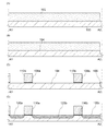
図6は、図2の回路図で示した半導体装置の、メモリセル190および選択トランジスタ180の構成の一例である。図6(A)には、半導体装置の断面を、図6(B)には、半導体装置の平面を、それぞれ示す。ここで、図6(A)は、図6(B)のA1−A2における断面に相当する。また、図6(B)において、A1−A2に平行な方向が図2の回路図における列方向であり、A1−A2に垂直な方向が図2の回路図における行方向である。図6(A)および図6(B)に示される半導体装置は、下部に第1の半導体材料を用いたトランジスタ160、選択トランジスタ180を有し、上部に第2の半導体材料を用いたトランジスタ162および容量素子164を有するものである。なお、図6では、第1行目のトランジスタ160およびトランジスタ162を表示しているが、図2の回路図に示すように、第1行目から第m行目までトランジスタ160とトランジスタ162は、ソース電極(ソース領域)とドレイン電極(ドレイン領域)が直列に接続されている。
<Cross-sectional configuration and planar configuration of semiconductor device>
6 illustrates an example of a structure of the
ここで、第1の半導体材料と第2の半導体材料とは異なる材料とすることが望ましい。例えば、第1の半導体材料を酸化物半導体以外の半導体材料(シリコンなど)とし、第2の半導体材料を酸化物半導体とすることができる。単結晶シリコンなどの酸化物半導体以外の材料を用いたトランジスタは、高速動作が容易である。一方で、酸化物半導体を用いたトランジスタは、その特性により長時間の電荷保持を可能とする。 Here, the first semiconductor material and the second semiconductor material are preferably different materials. For example, the first semiconductor material can be a semiconductor material other than an oxide semiconductor (such as silicon), and the second semiconductor material can be an oxide semiconductor. A transistor including a material other than an oxide semiconductor such as single crystal silicon can easily operate at high speed. On the other hand, a transistor including an oxide semiconductor can hold charge for a long time due to its characteristics.
なお、上記トランジスタは、いずれもnチャネル型トランジスタであるものとして説明するが、pチャネル型トランジスタを用いることができるのはいうまでもない。また、開示する発明の技術的な本質は、情報を保持するために酸化物半導体のようなオフ電流を十分に低減することが可能な半導体材料をトランジスタ162に用いる点にあるから、半導体装置に用いられる材料や半導体装置の構造など、半導体装置の具体的な構成をここで示すものに限定する必要はない。
Note that although all the above transistors are described as n-channel transistors, it goes without saying that p-channel transistors can be used. The technical essence of the disclosed invention is that a semiconductor material such as an oxide semiconductor that can sufficiently reduce off-state current is used for the
図6におけるトランジスタ160は、半導体材料(例えば、シリコンなど)を含む基板100に設けられたチャネル形成領域116aと、チャネル形成領域116aを挟むように設けられた不純物領域120aおよび不純物領域120bと、不純物領域120aおよび不純物領域120bに接する金属化合物領域124aおよび金属化合物領域124bと、チャネル形成領域116a上に設けられたゲート絶縁層108aと、ゲート絶縁層108a上に設けられたゲート電極110aと、を有する。なお、図において、明示的にはソース電極やドレイン電極を有しない場合があるが、便宜上、このような状態を含めてトランジスタと呼ぶ場合がある。また、この場合、トランジスタの接続関係を説明するために、ソース領域やドレイン領域を含めてソース電極やドレイン電極と表現することがある。つまり、本明細書において、ソース電極との記載にはソース領域が、ドレイン電極との記載にはドレイン領域が、含まれうる。
6 includes a
なお、本明細書中において、不純物領域120a、不純物領域120bおよび後述する不純物領域120cをまとめて、不純物領域120と記載する場合がある。また、本明細書中において、金属化合物領域124a、金属化合物領域124b、および後述する金属化合物領域124cをまとめて、金属化合物領域124と記載する場合がある。
Note that in this specification, the
ここで、トランジスタ160は、ソース領域またはドレイン領域として機能する不純物領域120および金属化合物領域124を共有して、第1行目から第m行目まで直列に接続される。つまり、第l−1行目(lは2以上m以下の自然数)のトランジスタ160のソース領域として機能する不純物領域120および金属化合物領域124は、第l行目のトランジスタ160のドレイン領域として機能することになる。このように、メモリセル190のトランジスタ160を直列に接続することによって、各メモリセル190間でトランジスタ160のソース領域およびドレイン領域を共有することができる。つまり、各メモリセル190において、トランジスタ160のソース領域またはドレイン領域の一方を、開口部を設けて、配線158に別途接続する必要がない。よって、トランジスタ160の平面レイアウトは、配線158と接続するための開口部を設ける必要がないので、後述するトランジスタ162の平面レイアウトに容易に重ねることができ、メモリセル190の占有面積の低減を図ることができる。
Here, the
また、第1行目のトランジスタ160は、選択トランジスタ180を介してビット線と電気的に接続されるので、第1行目のトランジスタ160のドレイン領域として機能する、不純物領域120bおよび金属化合物領域124bは、選択トランジスタ180のソース領域として機能する。ここで、選択トランジスタ180は、上述のトランジスタ160と同様の構成とすることができる。つまり、選択トランジスタ180は、半導体材料(例えば、シリコンなど)を含む基板100に設けられたチャネル形成領域116bと、チャネル形成領域116bを挟むように設けられた不純物領域120bおよび不純物領域120cと、不純物領域120bおよび不純物領域120cに接する金属化合物領域124bおよび金属化合物領域124cと、チャネル形成領域116b上に設けられたゲート絶縁層108bと、ゲート絶縁層108b上に設けられたゲート電極110bと、を有する。なお、選択トランジスタ180のゲート電極110bは、図2に示す回路図における、選択線G_1として機能する。
In addition, since the
なお、本明細書中において、チャネル形成領域116aおよびチャネル形成領域116bをまとめて、チャネル形成領域116と記載する場合がある。また、本明細書中において、ゲート絶縁層108aおよびゲート絶縁層108bをまとめて、ゲート絶縁層108と記載する場合がある。また、本明細書中において、ゲート電極110aおよびゲート電極110bをまとめて、ゲート電極110と記載する場合がある。
Note that in this specification, the
また、基板100上にはトランジスタ160および選択トランジスタ180を囲むように素子分離絶縁層106が設けられており、トランジスタ160および選択トランジスタ180上に、ゲート電極110の上面を露出させるように絶縁層128が設けられている。なお、高集積化を実現するためには、図6に示すようにトランジスタ160がサイドウォール絶縁層を有しない構成とすることが望ましい。一方で、トランジスタ160の特性を重視する場合には、ゲート電極110の側面にサイドウォール絶縁層を設け、不純物濃度が異なる領域を含む不純物領域120を設けても良い。
Further, an element
ここで、絶縁層128は、平坦性の良好な表面を有しているのが好ましく、例えば、絶縁層128の表面は、二乗平均平方根(RMS)粗さを1nm以下とすることが好ましい。
Here, the insulating
図6におけるトランジスタ162は、絶縁層128上に形成された絶縁層140に埋め込まれたソース電極142aおよびドレイン電極142bと、絶縁層140、ソース電極142aおよびドレイン電極142bの一部と接する酸化物半導体層144と、酸化物半導体層144を覆うゲート絶縁層146と、ゲート絶縁層146上に酸化物半導体層144と重畳するように設けられたゲート電極148と、を有する。なお、ゲート電極148は、図2に示す回路図における、信号線Sとして機能する。
6 includes an oxide semiconductor in contact with the
ここで、酸化物半導体層144は水素などの不純物が十分に除去されることにより、または、十分な酸素が供給されることにより、高純度化されたものであることが望ましい。具体的には、例えば、酸化物半導体層144の水素濃度は5×10¹⁹atoms/cm3以下、望ましくは5×1018atoms/cm3以下、より望ましくは5×1017atoms/cm3以下とする。なお、上述の酸化物半導体層144中の水素濃度は、二次イオン質量分析法(SIMS:Secondary Ion Mass Spectroscopy)で測定されるものである。このように、水素濃度が十分に低減されて高純度化され、十分な酸素の供給により酸素欠乏に起因するエネルギーギャップ中の欠陥準位が低減された酸化物半導体層144では、水素等のドナーに起因するキャリア密度が1×10¹²/cm3未満、望ましくは、1×1011/cm3未満、より望ましくは1.45×1010/cm3未満となる。また、例えば、室温(25℃)でのオフ電流(ここでは、単位チャネル幅(1μm)あたりの値)は100zA(1zA(ゼプトアンペア)は1×10−21A)以下、望ましくは10zA以下となる。このように、i型化(真性化)または実質的にi型化された(i型に限りなく近い)酸化物半導体を用いることで、極めて優れたオフ電流特性のトランジスタ162を得ることができる。
Here, it is preferable that the
また、絶縁層140の表面であって酸化物半導体層144と接する領域は、その二乗平均平方根(RMS)粗さを1nm以下とすることが好ましい。このように、二乗平均平方根(RMS)粗さが1nm以下という極めて平坦な領域にトランジスタ162のチャネル形成領域を設けることにより、トランジスタ162が微細化される状況においても、短チャネル効果などの不具合を防止し、良好な特性を有するトランジスタ162を提供することが可能である。
Further, it is preferable that the surface of the insulating
また、トランジスタ162は、ソース電極142aおよびドレイン電極142bをお互いに共有して、第1行目から第m行目まで直列に接続される。つまり、第l−1行目(lは2以上m以下の自然数)のトランジスタ162のソース電極142aと、第l行目のトランジスタ162のドレイン電極142bとは、同一の導電層で形成されることになる。
The
このように、メモリセル190のトランジスタ162を直列に接続することによって、各メモリセル190間でトランジスタ162のソース電極142aおよびドレイン電極142bをお互いに接続させることができる。これにより、メモリセル190の平面レイアウトには、トランジスタ162のソース電極142aまたはドレイン電極142bの一方のみが含まれることになる。つまり、メモリセル190の平面レイアウトの列方向の長さを、ゲート電極148の最小限の配線幅と配線間隔の長さ程度まで小さくすることができる。
In this manner, by connecting the
それに対して、メモリセル190のトランジスタ162を並列に接続し、各メモリセル190においてトランジスタ162のソース電極142aおよびドレイン電極142bを個別に設ける場合は、各メモリセル190において、トランジスタ162のソース電極142aまたはドレイン電極142bの一方を、開口部を設けて、配線158などの配線に別途接続する必要がある。よって、メモリセル190の平面レイアウトには、トランジスタ162のソース電極142a及びドレイン電極142bの両方と、配線と接続するための開口部とが含まれることになる。
On the other hand, when the
よって、メモリセル190の平面レイアウトを図6に示すような構成にすることにより、
メモリセル190の占有面積を低減することができる。例えば、最小加工寸法をFとして、メモリセル190の占有面積を4F2〜12F2とすることが可能である。以上より、半導体装置の高集積化を図り、単位面積あたりの記憶容量を増加させることができる。
Therefore, by configuring the planar layout of the
The area occupied by the
図6における容量素子164は、ソース電極142a、酸化物半導体層144、ゲート絶縁層146、ゲート絶縁層146上の絶縁層150および電極152、で構成される。すなわち、ソース電極142aは、容量素子164の一方の電極として機能し、電極152は、容量素子164の他方の電極として機能することになる。なお、容量素子164は、ゲート絶縁層146を含まない構成としてもよい。このような構成とすることにより、容量素子164の誘電体層は、酸化物半導体層144と絶縁層150で構成されることになるので、誘電体層の膜厚が低減され、容量素子164の静電容量を増加させることができる。
6 includes a
ここで、第l−1行目(lは2以上m以下の自然数)の容量素子164の一方の電極は、第l−1行目のトランジスタ162のソース電極142aなので、容量素子164の平面レイアウトは、トランジスタ162の平面レイアウトに容易に重ねることができ、メモリセル190の占有面積の低減を図ることができる。また、電極152を絶縁層150上に形成することで、隣り合うメモリセル190のゲート電極148を最小限の配線間隔で形成し、且つ隣り合うメモリセル190のゲート電極148の間に電極152を形成することができる。これにより、メモリセル190の占有面積の低減を図ることができる。なお、電極152は、図2に示す回路図における、ワード線WLとして機能する。
Here, since one electrode of the
トランジスタ162の上には、絶縁層150が設けられており、絶縁層150および容量素子164の電極152上には絶縁層154が設けられている。そして、ゲート絶縁層146、絶縁層150、絶縁層154などに形成された開口には、電極156aが設けられ、絶縁層154上には電極156aと接続する配線158が形成される。また、ゲート絶縁層146、絶縁層150、絶縁層154などに形成された開口に設けられた電極156bと、絶縁層140に埋め込まれた電極142cと、絶縁層128に埋め込まれた電極126と、を介して配線158と選択トランジスタ180のドレイン領域として機能する金属化合物領域124cとが電気的に接続される。ここで、配線158は、図2に示す回路図における、ビット線BLとして機能する。
An insulating
以上のような構成とすることにより、トランジスタ160、トランジスタ162および容量素子164からなる、メモリセル190の平面レイアウトの大きさを低減することができる。メモリセル190の平面レイアウトは、行方向の長さを、ビット線BLとして機能する配線158の最小限の配線幅と配線間隔の長さ程度まで小さくすることができ、列方向の長さは、ゲート電極148の最小限の配線幅と配線間隔の長さ程度まで小さくすることができる。このような平面レイアウトを採用することにより、図2に示す回路の高集積化を図ることができ、例えば、最小加工寸法をFとして、メモリセルの占有面積を4F2〜12F2とすることが可能である。よって、半導体装置の単位面積あたりの記憶容量を増加させることができる。
With the above structure, the size of the planar layout of the
なお、開示する発明に係る半導体装置の構成は、図6に示されるものに限定されない。開示する発明の一態様の技術的思想は、酸化物半導体と、酸化物半導体以外の材料と、を用いた積層構造を形成する点にあるから、電極の接続関係等の詳細については、適宜変更することができる。 Note that the structure of the semiconductor device according to the disclosed invention is not limited to that illustrated in FIGS. Since the technical idea of one embodiment of the disclosed invention is to form a stacked structure using an oxide semiconductor and a material other than the oxide semiconductor, details of electrode connection relations and the like are changed as appropriate. can do.
例えば、図3に示すように、選択線G_1および選択トランジスタ180を省略し、上記選択線G_2に相当する選択線Gと、選択トランジスタ182と、だけを設ける構成とする場合、ビット線BLと第1行目のメモリセル190の接続部分の構成の一例を、図7に示す。図7(A)には、半導体装置の断面を、図7(B)には、半導体装置の平面を、それぞれ示す。ここで、図7(A)は、図7(B)のB1−B2における断面に相当する。
For example, as shown in FIG. 3, when the selection line G_1 and the
図7に示す半導体装置と図6に示す半導体装置との相違点の一は、選択トランジスタ180が設けられているか否かである。よって、図7に示す半導体装置の詳細については、図6に示す半導体装置を参酌することができる。なお、図7に示す半導体装置の、図6に示す半導体装置と共通する部分については、同一の符号を用いている。
One of the differences between the semiconductor device shown in FIG. 7 and the semiconductor device shown in FIG. 6 is whether or not a
ただし、図6に示す半導体装置とは異なり、配線158とトランジスタ160とは、ゲート絶縁層146、絶縁層150、絶縁層154に形成された開口に設けられた電極156aと、絶縁層140に埋め込まれたドレイン電極142bと、絶縁層128に埋め込まれた電極126と、を介して電気的に接続される。
However, unlike the semiconductor device illustrated in FIG. 6, the
また、図6に示す半導体装置は、絶縁層140および、絶縁層140中に埋め込まれたソース電極142a、ドレイン電極142b上に酸化物半導体層144を設ける構成の半導体装置としたが、図8(A)に示すように、絶縁層140および、絶縁層140中に埋め込まれたソース電極142a、ドレイン電極142bを設けず、ゲート電極110aおよび絶縁層128上に直接酸化物半導体層144を設けるような構成としても良い。ここで、図8(A)には、半導体装置の断面図を示す。図8(A)に示す半導体装置と図6に示す半導体装置の主な相違点は、上述の絶縁層140、ソース電極142aおよびドレイン電極142bの有無である。なお、図8(A)に示す半導体装置の、図6に示す半導体装置と共通する部分については、同一の符号を用いている。
6 is the semiconductor device having the structure in which the insulating
ここで、図8(A)に示す半導体装置においては、ゲート電極110aがトランジスタ162のソース電極またはドレイン電極として機能するということもできる。つまり、第l−1行目(lは2以上m以下の自然数)のトランジスタ160のゲート電極110aと、第l−1行目のトランジスタ162のソース電極と、第l行目のトランジスタ162のドレイン電極とは、同一の導電層で形成されることになる。図6に示す半導体装置において、コンタクトの都合上、ソース電極142aよりゲート電極110aの方が列方向の長さが小さくなるので、ソース電極142aを設けない構造の図8(A)に示す半導体装置は、さらにメモリセル190の占有面積の縮小を図ることができる。
Here, in the semiconductor device illustrated in FIG. 8A, the
また、図8(A)に示す半導体装置においては、電極156aと酸化物半導体層144との間に電極159aを設けて、配線158と酸化物半導体層144とを電気的に接続するのが好ましい。このようにすることで、配線158と酸化物半導体層144とのコンタクトを容易且つ確実にとることができる。また、同様に、電極156bと電極126との間に電極159bを設けて、配線158と選択トランジスタ180の金属化合物領域124cとを電気的に接続してもよい。なお、電極159aおよび電極159bは、電極152と同時に形成することができる。
In the semiconductor device illustrated in FIG. 8A, it is preferable that the
また、図8(B)に示すように、SOI基板上にトランジスタ160および選択トランジスタ180を形成するような構成としても良い。ここで、図8(B)には、半導体装置の断面図を示す。図8(B)に示す半導体装置と図6に示す半導体装置の相違点の一は、トランジスタ160および選択トランジスタ180のチャネル形成領域116および不純物領域120がSOI基板に設けられた半導体層で構成されている点である。なお、図8(B)に示す半導体装置の、図6に示す半導体装置と共通する部分については、同一の符号を用いている。
Alternatively, as illustrated in FIG. 8B, a structure in which the
図8(B)に示すSOI基板は、ベース基板170と、ベース基板170上に形成された窒素含有層172と、窒素含有層172上に形成された酸化膜174と、酸化膜174上に形成された半導体層からなる。該半導体層は、トランジスタ160および選択トランジスタ180のチャネル形成領域116および不純物領域120を構成する。
The SOI substrate illustrated in FIG. 8B is formed over the
ここで、ベース基板170としては、絶縁体でなる基板を用いることができる。具体的には、アルミノシリケートガラス、アルミノホウケイ酸ガラス、バリウムホウケイ酸ガラスのような電子工業用に使われる各種ガラス基板、石英基板、セラミック基板、サファイア基板が挙げられる。また、窒化シリコンと酸化アルミニウムを主成分とした熱膨張係数がシリコンに近いセラミック基板を用いてもよい。
Here, as the
また、窒素含有層172としては、窒化シリコン膜(SiNx)や窒化酸化シリコン膜(SiNxOy)(x>y)等の窒素を含有する絶縁膜を含む層を用いることができる。また、酸化膜174は、酸化シリコン膜、酸化窒化シリコン膜等を単層で、または積層させて形成することができる。
As the nitrogen-containing
また、チャネル形成領域116および不純物領域120を構成する半導体層としては、単結晶シリコン基板、単結晶ゲルマニウム基板、単結晶シリコンゲルマニウム基板など、第14族元素でなる単結晶半導体基板を用いて形成された、膜厚が10nm以上500nm以下、好ましくは50nm以上200nm以下の半導体層とすればよい。
The semiconductor layer forming the channel formation region 116 and the
また、図6に示す半導体装置は、ソース電極142aおよびドレイン電極142bを絶縁層140中に埋め込む構成としたが、図8(B)に示すように、ソース電極142aおよびドレイン電極142bを絶縁層中に埋め込むことなく、ゲート電極110および絶縁層128上に設ける構成としても良い。ここで、ソース電極142aおよびドレイン電極142bの端部は、テーパー形状であることが好ましい。ソース電極142a、ドレイン電極142bの端部をテーパー形状とすることにより、酸化物半導体層144の被覆性を向上し、段切れを防止することができるためである。ここで、テーパー角は、例えば、30°以上60°以下とする。なお、テーパー角とは、テーパー形状を有する層(例えば、ソース電極142a)を、その断面(基板の表面と直交する面)に垂直な方向から観察した際に、当該層の側面と底面がなす傾斜角を示す。
In the semiconductor device illustrated in FIG. 6, the
〈半導体装置の作製方法〉
次に、上記半導体装置の作製方法の一例について説明する。以下では、はじめに下部のトランジスタ160および選択トランジスタ180の作製方法について図9および図10を参照して説明し、その後、上部のトランジスタ162および容量素子164の作製方法について図11および図12を参照して説明する。
<Method for Manufacturing Semiconductor Device>
Next, an example of a method for manufacturing the semiconductor device will be described. Hereinafter, a method for manufacturing the
〈下部のトランジスタの作製方法〉
まず、半導体材料を含む基板100を用意する(図9(A)参照)。半導体材料を含む基板100としては、シリコンや炭化シリコンなどの単結晶半導体基板、多結晶半導体基板、シリコンゲルマニウムなどの化合物半導体基板、SOI基板などを適用することができる。ここでは、半導体材料を含む基板100として、単結晶シリコン基板を用いる場合の一例について示すものとする。なお、一般に「SOI基板」は、絶縁表面上にシリコン半導体層が設けられた構成の基板をいうが、本明細書等においては、絶縁表面上にシリコン以外の材料からなる半導体層が設けられた構成の基板も含む概念として用いる。つまり、「SOI基板」が有する半導体層は、シリコン半導体層に限定されない。また、SOI基板には、ガラス基板などの絶縁基板上に絶縁層を介して半導体層が設けられた構成のものが含まれるものとする。
<Production method of lower transistor>
First, the
半導体材料を含む基板100として、特に、シリコンなどの単結晶半導体基板を用いる場合には、半導体装置の読み出し動作を高速化することができるため好適である。
In particular, when a single crystal semiconductor substrate such as silicon is used as the
なお、トランジスタのしきい値電圧を制御するために、後にトランジスタ160のチャネル形成領域116aおよび選択トランジスタ180のチャネル形成領域116bとなる領域に、不純物元素を添加しても良い。ここでは、トランジスタ160および選択トランジスタ180のしきい値電圧が正となるように導電性を付与する不純物元素を添加する。半導体材料がシリコンの場合、該導電性を付与する不純物には、例えば、硼素、アルミニウム、ガリウムなどがある。なお、不純物元素の添加後には、加熱処理を行い、不純物元素の活性化や不純物元素の添加時に生じる欠陥の改善等を図るのが望ましい。
Note that an impurity element may be added to a region which later becomes the
基板100上には、素子分離絶縁層を形成するためのマスクとなる保護層102を形成する(図9(A)参照)。保護層102としては、例えば、酸化シリコンや窒化シリコン、酸窒化シリコンなどを材料とする絶縁層を用いることができる。
A
次に、上記の保護層102をマスクとしてエッチングを行い、保護層102に覆われていない領域(露出している領域)の、基板100の一部を除去する。これにより他の半導体領域と分離された半導体領域104が形成される(図9(B)参照)。当該エッチングには、ドライエッチングを用いるのが好適であるが、ウェットエッチングを用いても良い。エッチングガスやエッチング液については被エッチング材料に応じて適宜選択することができる。
Next, etching is performed using the
次に、基板100を覆うように絶縁層を形成し、半導体領域104に重畳する領域の絶縁層を選択的に除去することで、素子分離絶縁層106を形成する(図9(C)参照)。当該絶縁層は、酸化シリコンや窒化シリコン、酸窒化シリコンなどを用いて形成される。絶縁層の除去方法としては、CMP(化学的機械的研磨)処理などの研磨処理やエッチング処理などがあるが、そのいずれを用いても良い。なお、半導体領域104の形成後、または、素子分離絶縁層106の形成後には、上記保護層102を除去する。
Next, an insulating layer is formed so as to cover the
次に、半導体領域104の表面に絶縁層を形成し、当該絶縁層上に導電材料を含む層を形成する。
Next, an insulating layer is formed on the surface of the
絶縁層は後のゲート絶縁層となるものであり、例えば、半導体領域104表面の熱処理(熱酸化処理や熱窒化処理など)によって形成することができる。熱処理に代えて、高密度プラズマ処理を適用しても良い。高密度プラズマ処理は、例えば、ヘリウム(He)、アルゴン(Ar)、クリプトン(Kr)、キセノン(Xe)などの希ガス、酸素、酸化窒素、アンモニア、窒素、水素などの混合ガスを用いて行うことができる。もちろん、CVD法やスパッタリング法等を用いて絶縁層を形成しても良い。当該絶縁層は、酸化シリコン、酸窒化シリコン、窒化シリコン、酸化ハフニウム、酸化アルミニウム、酸化タンタル、酸化イットリウム、ハフニウムシリケート(HfSixOy(x>0、y>0))、窒素が添加されたハフニウムシリケート(HfSixOyNz(x>0、y>0、z>0))、窒素が添加されたハフニウムアルミネート(HfAlxOyNz(x>0、y>0、z>0))等を含む単層構造または積層構造とすることが望ましい。また、絶縁層の厚さは、例えば、1nm以上100nm以下、好ましくは10nm以上50nm以下とすることができる。
The insulating layer will be a gate insulating layer later, and can be formed by, for example, heat treatment (thermal oxidation treatment, thermal nitridation treatment, or the like) on the surface of the
導電材料を含む層は、アルミニウムや銅、チタン、タンタル、タングステン等の金属材料を用いて形成することができる。また、多結晶シリコンなどの半導体材料を用いて、導電材料を含む層を形成しても良い。形成方法も特に限定されず、蒸着法、CVD法、スパッタリング法、スピンコート法などの各種成膜方法を用いることができる。なお、本実施の形態では、導電材料を含む層を、金属材料を用いて形成する場合の一例について示すものとする。 The layer including a conductive material can be formed using a metal material such as aluminum, copper, titanium, tantalum, or tungsten. Alternatively, a layer including a conductive material may be formed using a semiconductor material such as polycrystalline silicon. There is no particular limitation on the formation method, and various film formation methods such as an evaporation method, a CVD method, a sputtering method, and a spin coating method can be used. Note that in this embodiment, an example of the case where the layer including a conductive material is formed using a metal material is described.
その後、絶縁層および導電材料を含む層を選択的にエッチングして、ゲート絶縁層108(ゲート絶縁層108a、ゲート絶縁層108b)およびゲート電極110(ゲート電極110a、ゲート電極110b)を形成する(図9(C)参照)。
After that, the insulating layer and the layer containing a conductive material are selectively etched to form the gate insulating layer 108 (
次に、半導体領域104にリン(P)やヒ素(As)などを添加して、チャネル形成領域116(チャネル形成領域116a、チャネル形成領域116b)および不純物領域120(不純物領域120a、不純物領域120b、不純物領域120c)を形成する(図9(D)参照)。なお、ここではn型トランジスタを形成するためにリンやヒ素を添加しているが、p型トランジスタを形成する場合には、硼素(B)やアルミニウム(Al)などの不純物元素を添加すればよい。ここで、添加する不純物の濃度は適宜設定することができるが、半導体素子が高度に微細化される場合には、その濃度を高くすることが望ましい。
Next, phosphorus (P), arsenic (As), or the like is added to the
なお、ゲート電極110の周囲にサイドウォール絶縁層を形成して、不純物元素が異なる濃度で添加された不純物領域を形成しても良い。 Note that a sidewall insulating layer may be formed around the gate electrode 110 to form impurity regions to which impurity elements are added at different concentrations.
次に、ゲート電極110、不純物領域120等を覆うように金属層122を形成する(図10(A)参照)。当該金属層122は、真空蒸着法やスパッタリング法、スピンコート法などの各種成膜方法を用いて形成することができる。金属層122は、半導体領域104を構成する半導体材料と反応することによって低抵抗な金属化合物となる金属材料を用いて形成することが望ましい。このような金属材料としては、例えば、チタン、タンタル、タングステン、ニッケル、コバルト、白金等がある。
Next, a
次に、熱処理を施して、上記金属層122と半導体材料とを反応させる。これにより、不純物領域120(不純物領域120a、不純物領域120b、不純物領域120c)に接する金属化合物領域124(金属化合物領域124a、金属化合物領域124b、金属化合物領域124c)が形成される(図10(A)参照)。なお、ゲート電極110として多結晶シリコンなどを用いる場合には、ゲート電極110の金属層122と接触する部分にも、金属化合物領域が形成されることになる。
Next, heat treatment is performed to react the
上記熱処理としては、例えば、フラッシュランプの照射による熱処理を用いることができる。もちろん、その他の熱処理方法を用いても良いが、金属化合物の形成に係る化学反応の制御性を向上させるためには、ごく短時間の熱処理を実現できる方法を用いることが望ましい。なお、上記の金属化合物領域は、金属材料と半導体材料との反応により形成されるものであり、十分に導電性が高められた領域である。当該金属化合物領域を形成することで、電気抵抗を十分に低減し、素子特性を向上させることができる。なお、金属化合物領域124を形成した後には、金属層122は除去する。
As the heat treatment, for example, heat treatment by flash lamp irradiation can be used. Of course, other heat treatment methods may be used, but in order to improve the controllability of the chemical reaction related to the formation of the metal compound, it is desirable to use a method capable of realizing a heat treatment for a very short time. Note that the metal compound region is formed by a reaction between a metal material and a semiconductor material, and is a region in which conductivity is sufficiently increased. By forming the metal compound region, the electrical resistance can be sufficiently reduced and the device characteristics can be improved. Note that the
次に、選択トランジスタ180の金属化合物領域124c上に接するように電極126を形成する(図10(B)参照)。電極126は、スパッタ法をはじめとするPVD法や、プラズマCVD法などのCVD法を用いて導電層を形成した後、当該導電層をパターニングすることによって形成される。また、導電層の材料としては、アルミニウム、クロム、銅、タンタル、チタン、モリブデン、タングステンから選ばれた元素や、上述した元素を成分とする合金等を用いることができる。マンガン、マグネシウム、ジルコニウム、ベリリウム、ネオジム、スカンジウムのいずれか、またはこれらを複数組み合わせた材料を用いてもよい。詳細は、後述するソース電極142a、ドレイン電極142bなどと同様である。
Next, the
以上により、半導体材料を含む基板100を用いたトランジスタ160および選択トランジスタ180が形成される(図10(B)参照)。このようなトランジスタ160は、高速動作が可能であるという特徴を有する。このため、当該トランジスタを読み出し用のトランジスタとして用いることで、情報の読み出しを高速に行うことができる。
Through the above steps, the
次に、上述の工程により形成された各構成を覆うように、絶縁層128を形成する(図10(C)参照)。絶縁層128は、酸化シリコン、酸窒化シリコン、窒化シリコン、酸化アルミニウム等の無機絶縁材料を含む材料を用いて形成することができる。特に、絶縁層128に誘電率の低い(low−k)材料を用いることで、各種電極や配線の重なりに起因する容量を十分に低減することが可能になるため好ましい。なお、絶縁層128には、これらの材料を用いた多孔質の絶縁層を適用しても良い。多孔質の絶縁層では、密度の高い絶縁層と比較して誘電率が低下するため、電極や配線に起因する容量をさらに低減することが可能である。また、絶縁層128は、ポリイミド、アクリル等の有機絶縁材料を用いて形成することも可能である。なお、ここでは、絶縁層128を単層構造としているが、開示する発明の一態様はこれに限定されない。絶縁層128を2層以上の積層構造としても良い。
Next, the insulating
その後、トランジスタ162および容量素子164の形成前の処理として、絶縁層128にCMP処理を施して、ゲート電極110a、ゲート電極110bおよび電極126の上面を露出させる(図10(D)参照)。ゲート電極110の上面を露出させる処理としては、CMP処理の他にエッチング処理などを適用することも可能であるが、トランジスタ162の特性を向上させるために、絶縁層128の表面は可能な限り平坦にしておくことが望ましく、例えば、絶縁層128の表面は、二乗平均平方根(RMS)粗さを1nm以下とすることが好ましい。
After that, as treatment before formation of the
なお、上記の各工程の前後には、さらに電極や配線、半導体層、絶縁層などを形成する工程を含んでいても良い。例えば、配線の構造として、絶縁層および導電層の積層構造でなる多層配線構造を採用して、高度に集積化した半導体装置を実現することも可能である。 Note that before and after each of the above steps, a step of forming an electrode, a wiring, a semiconductor layer, an insulating layer, or the like may be further included. For example, a highly integrated semiconductor device can be realized by adopting a multilayer wiring structure including a laminated structure of an insulating layer and a conductive layer as a wiring structure.
〈上部のトランジスタの作製方法〉
次に、ゲート電極110、電極126、絶縁層128などの上に導電層を形成し、該導電層を選択的にエッチングして、ソース電極142a、ドレイン電極142b、電極142cを形成する(図11(A)参照)。
<Method for manufacturing upper transistor>
Next, a conductive layer is formed over the gate electrode 110, the
導電層は、スパッタ法をはじめとするPVD法や、プラズマCVD法などのCVD法を用いて形成することができる。また、導電層の材料としては、アルミニウム、クロム、銅、タンタル、チタン、モリブデン、タングステンからから選ばれた元素や、上述した元素を成分とする合金等を用いることができる。マンガン、マグネシウム、ジルコニウム、ベリリウム、ネオジム、スカンジウムのいずれか、またはこれらを複数組み合わせた材料を用いてもよい。 The conductive layer can be formed by a PVD method such as a sputtering method or a CVD method such as a plasma CVD method. As a material for the conductive layer, an element selected from aluminum, chromium, copper, tantalum, titanium, molybdenum, and tungsten, an alloy containing the above-described element as a component, or the like can be used. Any of manganese, magnesium, zirconium, beryllium, neodymium, scandium, or a combination of these may be used.
導電層は、単層構造であっても良いし、2層以上の積層構造としてもよい。例えば、チタン膜や窒化チタン膜の単層構造、シリコンを含むアルミニウム膜の単層構造、アルミニウム膜上にチタン膜が積層された2層構造、窒化チタン膜上にチタン膜が積層された2層構造、チタン膜とアルミニウム膜とチタン膜とが積層された3層構造などが挙げられる。なお、導電層を、チタン膜や窒化チタン膜の単層構造とする場合には、テーパー形状を有するソース電極142a、ドレイン電極142bおよび電極142cへの加工が容易であるというメリットがある。
The conductive layer may have a single layer structure or a stacked structure of two or more layers. For example, a single-layer structure of a titanium film or a titanium nitride film, a single-layer structure of an aluminum film containing silicon, a two-layer structure in which a titanium film is laminated on an aluminum film, or a two-layer structure in which a titanium film is laminated on a titanium nitride film Examples of the structure include a three-layer structure in which a titanium film, an aluminum film, and a titanium film are stacked. Note that in the case where the conductive layer has a single-layer structure of a titanium film or a titanium nitride film, there is an advantage that processing into the
また、導電層は、導電性の金属酸化物を用いて形成しても良い。導電性の金属酸化物としては酸化インジウム(In2O3)、酸化スズ(SnO2)、酸化亜鉛(ZnO)、酸化インジウム酸化スズ合金(In2O3−SnO2、ITOと略記する場合がある)、酸化インジウム酸化亜鉛合金(In2O3−ZnO)、または、これらの金属酸化物材料にシリコン若しくは酸化シリコンを含有させたものを用いることができる。 The conductive layer may be formed using a conductive metal oxide. The conductive metal oxide may be abbreviated as indium oxide (In 2 O 3 ), tin oxide (SnO 2 ), zinc oxide (ZnO), indium oxide tin oxide alloy (In 2 O 3 —SnO 2 , ITO). Indium oxide zinc oxide alloy (In 2 O 3 —ZnO), or a metal oxide material containing silicon or silicon oxide can be used.
なお、導電層のエッチングは、ドライエッチング、ウェットエッチングのいずれを用いて行っても良いが、微細化のためには、制御性の良いドライエッチングを用いるのが好適である。また、形成されるソース電極142a、およびドレイン電極142bがテーパー形状となるように行っても良い。テーパー角は、例えば、30°以上60°以下とすることができる。
Note that the etching of the conductive layer may be performed using either dry etching or wet etching, but it is preferable to use dry etching with good controllability for miniaturization. Alternatively, the
上部のトランジスタ162のチャネル長(L)は、ソース電極142a、およびドレイン電極142bの上端部の間隔によって決定される。なお、チャネル長(L)が25nm未満のトランジスタを形成する場合に用いるマスク形成の露光を行う際には、数nm〜数10nmと波長の短い超紫外線(Extreme Ultraviolet)を用いるのが望ましい。超紫外線による露光は、解像度が高く焦点深度も大きい。従って、後に形成されるトランジスタのチャネル長(L)を、2μm未満、好ましくは10nm以上350nm(0.35μm)以下とすることも可能であり、回路の動作速度を高めることが可能である。
The channel length (L) of the
なお、絶縁層128の上には、下地として機能する絶縁層を設けても良い。当該絶縁層は、PVD法やCVD法などを用いて形成することができる。
Note that an insulating layer functioning as a base may be provided over the insulating
次に、ソース電極142a、ドレイン電極142bおよび電極142cを覆うように絶縁層140を形成した後、ソース電極142a、ドレイン電極142bおよび電極142cが露出されるように、CMP(化学的機械的研磨)処理によって絶縁層140を平坦化する(図11(A)参照)。
Next, after the insulating
絶縁層140は、酸化シリコン、酸窒化シリコン、窒化シリコン、酸化アルミニウム、酸化ガリウム等の無機絶縁材料を含む材料を用いて形成することができる。絶縁層140には、後に酸化物半導体層144が接することになるから、例えば、酸化シリコンなどを用いたものにするのが好適である。なお、絶縁層140に、ガリウムやアルミニウムなど、酸化物半導体層144に含まれる可能性の高い13族元素を含ませる場合には、絶縁層140と酸化物半導体層144との界面特性を向上させて、水素のパイルアップなどを抑制し電気的特性を安定化することが可能になる。さらに、絶縁層140に酸化アルミニウムを用いる場合には、外部からの水の侵入を抑制することができるという効果もある。
The insulating
なお、酸化物半導体層144の酸素欠損に起因する欠陥の発生を抑制するという観点から、絶縁層140には、化学量論的組成より僅かに酸素が多く含まれる酸化物材料を用いると良い。このように、酸素を多く含む材料を酸化物半導体層144に接する層に用いることで、酸化物半導体層144に酸素を供給し、酸素欠損欠陥の発生を抑制して、トランジスタのノーマリーオン化を防ぐことができる。これにより、トランジスタを十分なオフ状態とするために必要な、ゲート端子とソース端子(またはドレイン端子)の電位差を小さくすることができるため、電位を変動させるために必要な消費電力を抑えることができる。または、半導体装置を適切に動作させることが容易になる。つまり、当該構成を適用する場合には、発明の一態様に係る効果は一層顕著になる。
Note that from the viewpoint of suppressing generation of defects due to oxygen vacancies in the
絶縁層140の形成方法に特に限定はないが、酸化物半導体層144と接することを考慮すれば、水素が十分に低減された方法によって形成するのが望ましい。このような方法としては、例えば、スパッタ法がある。もちろん、プラズマCVD法をはじめとする他の成膜法を用いても良い。また、絶縁層140の形成方法や、絶縁層140に対する処理などを工夫して、絶縁層140中に酸素が多く含まれるようにしても良い。例えば、成膜雰囲気に酸素を添加することで、酸素を多く含む絶縁層140を実現することができる。または、絶縁層140に対して、酸素雰囲気における熱処理や、酸素プラズマ処理などを適用しても良い。いずれにしても、絶縁層140の水素を十分に低減し、絶縁層140に十分な酸素を含ませることで、優れた特性の半導体装置を実現することができる。
There is no particular limitation on the formation method of the insulating
また、CMP(化学的機械的研磨)処理は、ソース電極142a、ドレイン電極142bおよび電極142cの表面の少なくとも一部が露出する条件で行う。また、当該CMP処理は、絶縁層140表面の二乗平均平方根(RMS)粗さが1nm以下(好ましくは0.5nm以下)となる条件で行うのが好ましい。このような条件でCMP処理を行うことにより、後に酸化物半導体層144が形成される表面の平坦性を向上させ、トランジスタ162の特性を向上させることができる。
Further, the CMP (Chemical Mechanical Polishing) process is performed under a condition that at least a part of the surface of the
なお、CMP処理は、1回のみ行ってもよいし、複数回行ってもよい。複数回に分けてCMP処理を行う場合は、高い研磨レートの一次研磨を行った後、低い研磨レートの仕上げ研磨を行うのが好ましい。このように研磨レートの異なる研磨を組み合わせることによって、絶縁層140の表面の平坦性をさらに向上させることができる。
The CMP process may be performed only once or a plurality of times. When performing the CMP process in a plurality of times, it is preferable to perform primary polishing at a low polishing rate after performing primary polishing at a high polishing rate. By combining polishing with different polishing rates in this way, the flatness of the surface of the insulating
次に、ソース電極142aの上面、ドレイン電極142bの上面、および絶縁層140の上面、の一部に接するように酸化物半導体層を形成した後、当該酸化物半導体層を選択的にエッチングして酸化物半導体層144を形成する(図11(B)参照)。
Next, an oxide semiconductor layer is formed so as to be in contact with part of the upper surface of the
酸化物半導体層144は、少なくともIn、Ga、Sn、Zn、Al、Mg、Hf及びランタノイドから選ばれた一種以上の元素を含有する。例えば、四元系金属の酸化物であるIn−Sn−Ga−Zn−O系酸化物半導体や、三元系金属の酸化物であるIn−Ga−Zn−O系酸化物半導体、In−Sn−Zn−O系酸化物半導体、In−Al−Zn−O系酸化物半導体、Sn−Ga−Zn−O系酸化物半導体、Al−Ga−Zn−O系酸化物半導体、Sn−Al−Zn−O系酸化物半導体、In−Hf−Zn−O系酸化物半導体、In−La−Zn−O系酸化物半導体、In−Ce−Zn−O系酸化物半導体、In−Pr−Zn−O系酸化物半導体、In−Nd−Zn−O系酸化物半導体、In−Pm−Zn−O系酸化物半導体、In−Sm−Zn−O系酸化物半導体、In−Eu−Zn−O系酸化物半導体、In−Gd−Zn−O系酸化物半導体、In−Tb−Zn−O系酸化物半導体、In−Dy−Zn−O系酸化物半導体、In−Ho−Zn−O系酸化物半導体、In−Er−Zn−O系酸化物半導体、In−Tm−Zn−O系酸化物半導体、In−Yb−Zn−O系酸化物半導体、In−Lu−Zn−O系酸化物半導体や、二元系金属の酸化物であるIn−Zn−O系酸化物半導体、Sn−Zn−O系酸化物半導体、Al−Zn−O系酸化物半導体、Zn−Mg−O系酸化物半導体、Sn−Mg−O系酸化物半導体、In−Mg−O系酸化物半導体や、In−Ga−O系の材料、一元系金属の酸化物であるIn−O系酸化物半導体、Sn−O系酸化物半導体、Zn−O系酸化物半導体などを用いることができる。また、上記酸化物半導体にInとGaとSnとZn以外の元素、例えばSiO2を含ませてもよい。
The
例えば、In−Ga−Zn−O系酸化物半導体とは、インジウム(In)、ガリウム(Ga)、亜鉛(Zn)を有する酸化物半導体、という意味であり、その組成比は問わない。 For example, an In—Ga—Zn—O-based oxide semiconductor means an oxide semiconductor containing indium (In), gallium (Ga), and zinc (Zn), and there is no limitation on the composition ratio.
中でも、In−Ga−Zn−O系の酸化物半導体材料は、無電界時の抵抗が十分に高くオフ電流を十分に小さくすることが可能であり、また、電界効果移動度も高いため、半導体装置に用いる半導体材料としては好適である。 Among them, an In—Ga—Zn—O-based oxide semiconductor material has a sufficiently high resistance when no electric field is applied and can have a sufficiently small off-state current. It is suitable as a semiconductor material used for the apparatus.
In−Ga−Zn−O系の酸化物半導体材料の代表例としては、InGaO3(ZnO)m(m>0)で表記されるものがある。また、Gaに代えてMの表記を用い、InMO3(ZnO)m(m>0)のように表記される酸化物半導体材料がある。ここで、Mは、ガリウム(Ga)、アルミニウム(Al)、鉄(Fe)、ニッケル(Ni)、マンガン(Mn)、コバルト(Co)などから選ばれた一の金属元素または複数の金属元素を示す。例えば、Mとしては、Ga、GaおよびAl、GaおよびFe、GaおよびNi、GaおよびMn、GaおよびCoなどを適用することができる。なお、上述の組成は結晶構造から導き出されるものであり、あくまでも一例に過ぎないことを付記する。 As a typical example of the In—Ga—Zn—O-based oxide semiconductor material, one represented by InGaO 3 (ZnO) m (m> 0) is given. In addition, there is an oxide semiconductor material in which M is used instead of Ga and is expressed as InMO 3 (ZnO) m (m> 0). Here, M represents one metal element or a plurality of metal elements selected from gallium (Ga), aluminum (Al), iron (Fe), nickel (Ni), manganese (Mn), cobalt (Co), and the like. Show. For example, as M, Ga, Ga and Al, Ga and Fe, Ga and Ni, Ga and Mn, Ga and Co, and the like can be applied. It should be noted that the above composition is derived from the crystal structure and is merely an example.
また、酸化物半導体としてIn−Zn−O系の材料を用いる場合、用いるターゲットの組成比は、原子数比で、In:Zn=50:1〜1:2(モル数比に換算するとIn2O3:ZnO=25:1〜1:4)、好ましくはIn:Zn=20:1〜1:1(モル数比に換算するとIn2O3:ZnO=10:1〜1:2)、さらに好ましくはIn:Zn=15:1〜1.5:1(モル数比に換算するとIn2O3:ZnO=15:2〜3:4)とする。例えば、In−Zn−O系酸化物半導体の形成に用いるターゲットは、原子数比がIn:Zn:O=X:Y:Zのとき、Z>1.5X+Yとする。 In the case where an In—Zn—O-based material is used as the oxide semiconductor, the composition ratio of the target used is an atomic ratio, and In: Zn = 50: 1 to 1: 2 (in terms of the molar ratio, In 2 O 3 : ZnO = 25: 1 to 1: 4), preferably In: Zn = 20: 1 to 1: 1 (In 2 O 3 : ZnO = 10: 1 to 1: 2 in terms of molar ratio), More preferably, In: Zn = 15: 1 to 1.5: 1 (In 2 O 3 : ZnO = 15: 2 to 3: 4 in terms of molar ratio). For example, a target used for forming an In—Zn—O-based oxide semiconductor satisfies Z> 1.5X + Y when the atomic ratio is In: Zn: O = X: Y: Z.
酸化物半導体層144をスパッタ法で作製するためのターゲットとしては、In:Ga:Zn=1:x:y(xは0以上、yは0.5以上5以下)の組成比で表されるものを用いるのが好適である。例えば、In2O3:Ga2O3:ZnO=1:1:2[mol数比]の組成比を有するターゲットなどを用いることができる。また、In2O3:Ga2O3:ZnO=1:1:1[mol数比](x=1、y=0.5)の組成比を有するターゲットや、In2O3:Ga2O3:ZnO=1:1:4[mol数比](x=1、y=2)の組成比を有するターゲットや、In2O3:Ga2O3:ZnO=1:0:2[mol数比](x=0、y=1)の組成比を有するターゲットを用いることもできる。
A target for forming the
本実施の形態では、非晶質構造の酸化物半導体層144を、In−Ga−Zn−O系の金属酸化物ターゲットを用いるスパッタ法により形成することとする。また、その膜厚は、1nm以上50nm以下、好ましくは2nm以上20nm以下、より好ましくは3nm以上15nm以下とする。
In this embodiment, the
金属酸化物ターゲット中の金属酸化物の相対密度は80%以上、好ましくは95%以上、さらに好ましくは99.9%以上である。相対密度の高い金属酸化物ターゲットを用いることにより、緻密な構造の酸化物半導体層を形成することが可能である。 The relative density of the metal oxide in the metal oxide target is 80% or more, preferably 95% or more, more preferably 99.9% or more. By using a metal oxide target with a high relative density, an oxide semiconductor layer with a dense structure can be formed.
酸化物半導体層144の形成雰囲気は、希ガス(代表的にはアルゴン)雰囲気、酸素雰囲気、または、希ガス(代表的にはアルゴン)と酸素との混合雰囲気とするのが好適である。具体的には、例えば、水素、水、水酸基、水素化物などの不純物が、1ppm以下(望ましくは10ppb以下)にまで除去された高純度ガス雰囲気を用いるのが好適である。
The atmosphere in which the
酸化物半導体層144の形成の際には、例えば、減圧状態に保たれた処理室内に被処理物を保持し、被処理物の温度が100℃以上550℃未満、好ましくは200℃以上400℃以下となるように被処理物を熱する。または、酸化物半導体層144の形成の際の被処理物の温度は、室温(25℃±10℃、15℃以上35℃以下)としてもよい。そして、処理室内の水分を除去しつつ、水素や水などが除去されたスパッタガスを導入し、上記ターゲットを用いて酸化物半導体層144を形成する。被処理物を熱しながら酸化物半導体層144を形成することにより、酸化物半導体層144に含まれる不純物を低減することができる。また、スパッタによる損傷を軽減することができる。処理室内の水分を除去するためには、吸着型の真空ポンプを用いることが好ましい。例えば、クライオポンプ、イオンポンプ、チタンサブリメーションポンプなどを用いることができる。また、ターボポンプにコールドトラップを加えたものを用いてもよい。クライオポンプなどを用いて排気することで、処理室から水素や水などを除去することができるため、酸化物半導体層中の不純物濃度を低減できる。
When the
酸化物半導体層144の形成条件としては、例えば、被処理物とターゲットの間との距離が170mm、圧力が0.4Pa、直流(DC)電力が0.5kW、雰囲気が酸素(酸素100%)雰囲気、またはアルゴン(アルゴン100%)雰囲気、または酸素とアルゴンの混合雰囲気、といった条件を適用することができる。なお、パルス直流(DC)電源を用いると、ごみ(成膜時に形成される粉状の物質など)を低減でき、膜厚分布も均一となるため好ましい。酸化物半導体層144の厚さは、1nm以上50nm以下、好ましくは2nm以上20nm以下、より好ましくは3nm以上15nm以下とする。開示する発明に係る構成を採用することで、このような厚さの酸化物半導体層144を用いる場合であっても、微細化に伴う短チャネル効果を抑制することが可能である。ただし、適用する酸化物半導体材料や、半導体装置の用途などにより適切な厚さは異なるから、その厚さは、用いる材料や用途などに応じて選択することもできる。
As a formation condition of the
なお、上記のように絶縁層140を形成することにより、酸化物半導体層144のチャネル形成領域に相当する部分の形成表面を十分に平坦化することができるので、厚みの小さい酸化物半導体層であっても、好適に形成することが可能である。また、図11(B)に示すように、酸化物半導体層144のチャネル形成領域に相当する部分の断面形状を、平坦な形状とすることが好ましい。酸化物半導体層144のチャネル形成領域に相当する部分の断面形状を平坦な形状とすることすることにより、酸化物半導体層144の断面形状が平坦でない場合と比較して、リーク電流を低減することができる。
Note that by forming the insulating
なお、酸化物半導体層144をスパッタ法により形成する前には、アルゴンガスを導入してプラズマを発生させる逆スパッタを行い、形成表面(例えば絶縁層140の表面)の付着物を除去しても良い。ここで、逆スパッタとは、通常のスパッタにおいては、スパッタターゲットにイオンを衝突させるところを、逆に、処理表面にイオンを衝突させることによってその表面を改質する方法のことをいう。処理表面にイオンを衝突させる方法としては、アルゴン雰囲気下で処理表面側に高周波電圧を印加して、被処理物付近にプラズマを生成する方法などがある。なお、アルゴン雰囲気に代えて窒素、ヘリウム、酸素などによる雰囲気を適用してもよい。
Note that before the
酸化物半導体層144の形成後には、酸化物半導体層144に対して熱処理(第1の熱処理)を行うことが望ましい。この第1の熱処理によって酸化物半導体層144中の、過剰な水素、水、水酸基などを除去し、酸化物半導体層144の構造を整え、エネルギーギャップ中の欠陥準位を低減することができる。第1の熱処理の温度は、例えば、300℃以上550℃未満、好ましくは400℃以上500℃以下とする。
After the
熱処理は、例えば、抵抗発熱体などを用いた電気炉に被処理物を導入し、窒素雰囲気下、450℃、1時間の条件で行うことができる。この間、酸化物半導体層は大気に触れさせず、水や水素の混入が生じないようにする。 The heat treatment can be performed, for example, by introducing an object to be processed into an electric furnace using a resistance heating element and the like under a nitrogen atmosphere at 450 ° C. for 1 hour. During this time, the oxide semiconductor layer is not exposed to the air so that water and hydrogen are not mixed.
熱処理装置は電気炉に限られず、加熱されたガスなどの媒体からの熱伝導、または熱輻射によって、被処理物を加熱する装置を用いても良い。例えば、LRTA(Lamp Rapid Thermal Anneal)装置、GRTA(Gas Rapid Thermal Anneal)装置等のRTA(Rapid Thermal Anneal)装置を用いることができる。LRTA装置は、ハロゲンランプ、メタルハライドランプ、キセノンアークランプ、カーボンアークランプ、高圧ナトリウムランプ、高圧水銀ランプなどのランプから発する光(電磁波)の輻射により、被処理物を加熱する装置である。GRTA装置は、高温のガスを用いて熱処理を行う装置である。ガスとしては、アルゴンなどの希ガス、または窒素のような、熱処理によって被処理物と反応しない不活性気体が用いられる。 The heat treatment apparatus is not limited to an electric furnace, and an apparatus for heating an object to be processed by heat conduction or heat radiation from a medium such as a heated gas may be used. For example, an RTA (Rapid Thermal Annial) apparatus such as an LRTA (Lamp Rapid Thermal Anneal) apparatus or a GRTA (Gas Rapid Thermal Anneal) apparatus can be used. The LRTA apparatus is an apparatus that heats an object to be processed by radiation of light (electromagnetic waves) emitted from a lamp such as a halogen lamp, a metal halide lamp, a xenon arc lamp, a carbon arc lamp, a high pressure sodium lamp, or a high pressure mercury lamp. The GRTA apparatus is an apparatus that performs heat treatment using a high-temperature gas. As the gas, an inert gas that does not react with an object to be processed by heat treatment, such as nitrogen or a rare gas such as argon, is used.
例えば、第1の熱処理として、熱せられた不活性ガス雰囲気中に被処理物を投入し、数分間熱した後、当該不活性ガス雰囲気から被処理物を取り出すGRTA処理を行ってもよい。GRTA処理を用いると短時間での高温熱処理が可能となる。また、被処理物の耐熱温度を超える温度条件であっても適用が可能となる。なお、処理中に、不活性ガスを、酸素を含むガスに切り替えても良い。酸素を含む雰囲気において第1の熱処理を行うことで、酸素欠損に起因するエネルギーギャップ中の欠陥準位を低減することができるためである。 For example, as the first heat treatment, a GRTA process may be performed in which an object to be processed is put in a heated inert gas atmosphere and heated for several minutes, and then the object to be processed is extracted from the inert gas atmosphere. When GRTA treatment is used, high-temperature heat treatment can be performed in a short time. In addition, application is possible even under temperature conditions exceeding the heat resistance temperature of the object to be processed. Note that the inert gas may be switched to a gas containing oxygen during the treatment. This is because the defect level in the energy gap due to oxygen deficiency can be reduced by performing the first heat treatment in an atmosphere containing oxygen.
なお、不活性ガス雰囲気としては、窒素、または希ガス(ヘリウム、ネオン、アルゴン等)を主成分とする雰囲気であって、水、水素などが含まれない雰囲気を適用するのが望ましい。例えば、熱処理装置に導入する窒素や、ヘリウム、ネオン、アルゴン等の希ガスの純度を、6N(99.9999%)以上、好ましくは7N(99.99999%)以上(すなわち、不純物濃度が1ppm以下、好ましくは0.1ppm以下)とする。 Note that as the inert gas atmosphere, an atmosphere containing nitrogen or a rare gas (such as helium, neon, or argon) as a main component and not including water, hydrogen, or the like is preferably used. For example, the purity of nitrogen or a rare gas such as helium, neon, or argon introduced into the heat treatment apparatus is 6N (99.9999%) or more, preferably 7N (99.99999%) or more (that is, the impurity concentration is 1 ppm or less). , Preferably 0.1 ppm or less).
いずれにしても、第1の熱処理によって不純物を低減し、i型(真性半導体)またはi型に限りなく近い酸化物半導体層を形成することで、極めて優れた特性のトランジスタを実現することができる。 In any case, a transistor with extremely excellent characteristics can be realized by reducing impurities by the first heat treatment and forming an oxide semiconductor layer that is almost i-type (intrinsic semiconductor) or i-type. .
ところで、上述の熱処理(第1の熱処理)には水素や水などを除去する効果があるから、当該熱処理を、脱水化処理や、脱水素化処理などと呼ぶこともできる。当該脱水化処理や、脱水素化処理は、酸化物半導体層144の形成後や後に形成するゲート絶縁層146の形成後、ゲート電極の形成後、などのタイミングにおいて行うことも可能である。また、このような脱水化処理、脱水素化処理は、一回に限らず複数回行っても良い。
By the way, since the above heat treatment (first heat treatment) has an effect of removing hydrogen, water, and the like, the heat treatment can be referred to as dehydration treatment, dehydrogenation treatment, or the like. The dehydration treatment or dehydrogenation treatment can be performed at the timing after the
酸化物半導体層144のエッチングは、上記熱処理の前、または上記熱処理の後のいずれにおいて行っても良い。また、素子の微細化という観点からはドライエッチングを用いるのが好適であるが、ウェットエッチングを用いても良い。エッチングガスやエッチング液については被エッチング材料に応じて適宜選択することができる。なお、素子におけるリークなどが問題とならない場合には、酸化物半導体層を島状に加工しないで用いても良い。
The etching of the
次に、酸化物半導体層144を覆うようにゲート絶縁層146を形成する(図11(C)参照)。
Next, the
ゲート絶縁層146は、CVD法やスパッタ法等を用いて形成することができる。また、ゲート絶縁層146は、酸化シリコン、窒化シリコン、酸窒化シリコン、酸化アルミニウム、酸化ガリウム、酸化タンタル、酸化ハフニウム、酸化イットリウム、ハフニウムシリケート(HfSixOy(x>0、y>0))、窒素が添加されたハフニウムシリケート(HfSixOyNz(x>0、y>0、z>0))、窒素が添加されたハフニウムアルミネート(HfAlxOyNz(x>0、y>0、z>0))、などを含むように形成するのが好適である。
The
なお、ゲート絶縁層146に、ガリウムやアルミニウムなど、酸化物半導体層144に含まれる可能性の高い13族元素を含ませる場合には、ゲート絶縁層146と酸化物半導体層144との界面特性を向上させて、水素のパイルアップなどを抑制し電気的特性を安定化することが可能になる。さらに、ゲート絶縁層146に酸化アルミニウムを用いる場合には、外部からの水の侵入を抑制することができるという効果もある。
Note that in the case where the
なお、酸化物半導体層144の酸素欠損に起因する欠陥の発生を抑制するという観点から、ゲート絶縁層146には、化学量論的組成より僅かに酸素が多く含まれる酸化物材料を用いると良い。このように、酸素を多く含む材料を酸化物半導体層144に接する層に用いることで、酸化物半導体層144に酸素を供給し、酸素欠損欠陥の発生を抑制して、トランジスタのノーマリーオン化を防ぐことができる。これにより、トランジスタを十分なオフ状態とするために必要な、ゲート端子とソース端子(またはドレイン端子)の電位差を小さくすることができるため、電位を変動させるために必要な消費電力を抑えることができる。または、半導体装置を適切に動作させることが容易になる。つまり、当該構成を適用する場合には、発明の一態様に係る効果は一層顕著になる。
Note that from the viewpoint of suppressing generation of defects due to oxygen vacancies in the
なお、ゲート絶縁層146は、水素が十分に低減された方法によって形成するのが望ましい。また、ゲート絶縁層146の形成方法や、ゲート絶縁層146に対する処理などを工夫して、ゲート絶縁層146中に酸素が多く含まれるようにしても良い。例えば、成膜雰囲気に酸素を添加することで、酸素を多く含むゲート絶縁層146を実現することができる。または、ゲート絶縁層146に対して、酸素雰囲気における熱処理や、酸素プラズマ処理などを適用しても良い。いずれにしても、ゲート絶縁層146の水素を十分に低減し、ゲート絶縁層146に十分な酸素を含ませることで、優れた特性の半導体装置を実現することができる。
Note that the
ゲート絶縁層146は、単層構造としても良いし、積層構造としても良い。また、その厚さは特に限定されないが、半導体装置を微細化する場合には、トランジスタの動作を確保するために薄くするのが望ましい。例えば、酸化シリコンを用いる場合には、1nm以上100nm以下、好ましくは10nm以上50nm以下とすることができる。
The
上述のように、ゲート絶縁層を薄くすると、トンネル効果などに起因するゲートリークが問題となる。ゲートリークの問題を解消するには、ゲート絶縁層146に、酸化ハフニウム、酸化タンタル、酸化イットリウム、ハフニウムシリケート(HfSixOy(x>0、y>0))、窒素が添加されたハフニウムシリケート(HfSixOyNz(x>0、y>0、z>0))、窒素が添加されたハフニウムアルミネート(HfAlxOyNz(x>0、y>0、z>0))、などの高誘電率(high−k)材料を用いると良い。high−k材料をゲート絶縁層146に用いることで、電気的特性を確保しつつ、ゲートリークを抑制するために膜厚を大きくすることが可能になる。例えば、酸化ハフニウムは比誘電率が15程度であり、酸化シリコンの比誘電率の3〜4と比較して非常に大きな値を有している。このような材料を用いることにより、酸化シリコン換算で15nm未満、好ましくは2nm以上10nm以下のゲート絶縁層を実現することも容易になる。なお、high−k材料を含む膜と、酸化シリコン、窒化シリコン、酸化窒化シリコン、窒化酸化シリコン、酸化アルミニウム、酸化ガリウムなどのいずれかを含む膜との積層構造としてもよい。
As described above, when the gate insulating layer is thin, gate leakage due to the tunnel effect or the like becomes a problem. In order to solve the problem of gate leakage, hafnium silicate in which hafnium oxide, tantalum oxide, yttrium oxide, hafnium silicate (HfSi x O y (x> 0, y> 0)) or nitrogen is added to the
ゲート絶縁層146の形成後には、不活性ガス雰囲気下、または酸素雰囲気下で第2の熱処理を行うのが望ましい。熱処理の温度は、200℃以上450℃以下、望ましくは250℃以上350℃以下である。例えば、窒素雰囲気下で250℃、1時間の熱処理を行えばよい。第2の熱処理を行うことによって、トランジスタの電気的特性のばらつきを軽減することができる。また、ゲート絶縁層146が酸素を含む場合、酸化物半導体層144に酸素を供給し、該酸化物半導体層144の酸素欠損を補填して、i型(真性半導体)またはi型に限りなく近い酸化物半導体層を形成することもできる。
After the
なお、本実施の形態では、ゲート絶縁層146の形成後に第2の熱処理を行っているが、第2の熱処理のタイミングはこれに限定されない。例えば、ゲート電極の形成後に第2の熱処理を行っても良い。また、第1の熱処理に続けて第2の熱処理を行っても良いし、第1の熱処理に第2の熱処理を兼ねさせても良いし、第2の熱処理に第1の熱処理を兼ねさせても良い。
Note that in this embodiment, the second heat treatment is performed after the
上述のように、第1の熱処理と第2の熱処理の少なくとも一方を適用することで、酸化物半導体層144を、その主成分以外の不純物が極力含まれないように高純度化することができる。
As described above, by applying at least one of the first heat treatment and the second heat treatment, the
次に、ゲート絶縁層146上にゲート電極148を形成する(図11(D)参照)。
Next, a
ゲート電極148は、ゲート絶縁層146上に導電層を形成した後に、当該導電層を選択的にエッチングすることによって形成することができる。ゲート電極148となる導電層は、スパッタ法をはじめとするPVD法や、プラズマCVD法などのCVD法を用いて形成することができる。詳細は、ソース電極142aまたはドレイン電極142bなどの場合と同様であり、これらの記載を参酌できる。
The
以上により、高純度化された酸化物半導体層144を用いたトランジスタ162が完成する(図11(D)参照)。このようなトランジスタ162は、オフ電流が十分低減されているという特徴を有する。このため、当該トランジスタを書き込み用のトランジスタとして用いることで、長時間の電荷保持を行うことができる。
Through the above steps, the
次に、ゲート絶縁層146およびゲート電極148上に、絶縁層150を形成する(図12(A)参照)。絶縁層150は、PVD法やCVD法などを用いて形成することができる。また、酸化シリコン、酸窒化シリコン、窒化シリコン、酸化ハフニウム、酸化アルミニウム等の無機絶縁材料を含む材料を用いて、単層または積層で形成することができる。
Next, the insulating
なお、絶縁層150には、誘電率の低い材料や、誘電率の低い構造(多孔質の構造など)を用いることが望ましい。絶縁層150の誘電率を低くすることにより、配線や電極などの間に生じる容量を低減し、動作の高速化を図ることができるためである。
Note that the insulating
なお、容量素子164に、ゲート絶縁層146を含まない構成とする場合は、絶縁層150を成膜する前に、ソース電極142a上の、容量素子164を形成する領域のゲート絶縁層146を除去すればよい。
Note that in the case where the
次に、ソース電極142aと重畳するように、絶縁層150上に電極152を形成する(図12(B)参照)。電極152は、ゲート電極148と同様の方法および材料で形成することができるので、詳細は、上記ゲート電極148の記載を参酌することができる。以上により、容量素子164が完成する。
Next, the
次に、絶縁層150および電極152上に、絶縁層154を形成する(図12(C)参照)。絶縁層154は、絶縁層150と同様に、PVD法やCVD法などを用いて形成することができる。また、酸化シリコン、酸窒化シリコン、窒化シリコン、酸化ハフニウム、酸化アルミニウム等の無機絶縁材料を含む材料を用いて、単層または積層で形成することができる。
Next, the insulating
なお、絶縁層154には、誘電率の低い材料や、誘電率の低い構造(多孔質の構造など)を用いることが望ましい。絶縁層154の誘電率を低くすることにより、配線や電極などの間に生じる容量を低減し、動作の高速化を図ることができるためである。
Note that the insulating
なお、上記絶縁層154は、その表面が平坦になるように形成することが望ましい。表面が平坦になるように絶縁層154を形成することで、半導体装置を微細化した場合などにおいても、絶縁層154上に、電極や配線などを好適に形成することができるためである。なお、絶縁層154の平坦化は、CMP(化学的機械的研磨)などの方法を用いて行うことができる。
Note that the insulating
次に、ゲート絶縁層146、絶縁層150、絶縁層154に、ドレイン電極142bにまで達する開口と、電極142cにまで達する開口とを形成した後、開口に電極156aおよび電極156bを形成し、絶縁層154上に、電極156aおよび電極156bに接する配線158を形成する(図12(D)参照)。当該開口の形成は、マスクなどを用いた選択的なエッチングにより行われる。
Next, an opening reaching the
電極156aおよび電極156bは、例えば、開口を含む領域にPVD法やCVD法などを用いて導電層を形成した後、エッチング処理やCMPといった方法を用いて、上記導電層の一部を除去することにより形成することができる。
For the
より具体的には、例えば、開口を含む領域にPVD法によりチタン膜を薄く形成し、CVD法により窒化チタン膜を薄く形成した後に、開口に埋め込むようにタングステン膜を形成する方法を適用することができる。ここで、PVD法により形成されるチタン膜は、被形成面の酸化膜(自然酸化膜など)を還元し、下部電極など(ここではドレイン電極142b)との接触抵抗を低減させる機能を有する。また、その後に形成される窒化チタン膜は、導電性材料の拡散を抑制するバリア機能を備える。また、チタンや窒化チタンなどによるバリア膜を形成した後に、メッキ法により銅膜を形成してもよい。
More specifically, for example, a method in which a titanium film is thinly formed by a PVD method in a region including an opening, a titanium nitride film is thinly formed by a CVD method, and then a tungsten film is formed so as to be embedded in the opening is applied. Can do. Here, the titanium film formed by the PVD method has a function of reducing an oxide film (a natural oxide film or the like) on a surface to be formed and reducing a contact resistance with a lower electrode or the like (here, the
配線158は、スパッタ法をはじめとするPVD法や、プラズマCVD法などのCVD法を用いて導電層を形成した後、当該導電層をパターニングすることによって形成される。また、導電層の材料としては、アルミニウム、クロム、銅、タンタル、チタン、モリブデン、タングステンから選ばれた元素や、上述した元素を成分とする合金等を用いることができる。マンガン、マグネシウム、ジルコニウム、ベリリウム、ネオジム、スカンジウムのいずれか、またはこれらを複数組み合わせた材料を用いてもよい。詳細は、ソース電極142aなどと同様である。
The
なお、上記工程の後に、各種配線や電極などを形成しても良い。配線や電極は、いわゆるダマシン法や、デュアルダマシン法などの方法を用いて形成することができる。 Note that various wirings, electrodes, and the like may be formed after the above steps. The wiring and the electrode can be formed using a so-called damascene method or a dual damascene method.
以上の工程より、図6に示すような構成の半導体装置を作製することができる。 Through the above steps, a semiconductor device having a structure as shown in FIG. 6 can be manufactured.
本実施の形態において示すトランジスタ162では、酸化物半導体層144が高純度化されているため、その水素濃度は、5×10¹⁹atoms/cm3以下、望ましくは5×1018atoms/cm3以下、より望ましくは5×1017atoms/cm3以下である。また、酸化物半導体層144のキャリア密度は、一般的なシリコンウェハにおけるキャリア密度(1×1014/cm3程度)と比較して、十分に小さい値(例えば、1×1012/cm3未満、より好ましくは、1.45×1010/cm3未満)をとる。そして、トランジスタ162のオフ電流も十分に小さくなる。例えば、トランジスタ162の室温(25℃)でのオフ電流(ここでは、単位チャネル幅(1μm)あたりの値)は100zA(1zA(ゼプトアンペア)は1×10−21A)以下、望ましくは10zA以下となる。
In the
このように高純度化され、真性化された酸化物半導体層144を用いることで、トランジスタ162のオフ電流を十分に低減することが容易になる。そして、このようなトランジスタ162を用いることで、極めて長期にわたり記憶内容を保持することが可能な半導体装置が得られる。
By using the highly purified and intrinsic
また、本実施の形態に示す半導体装置では、半導体装置の各メモリセルを構成する、酸化物半導体を用いたトランジスタを直列に接続することにより、隣接するメモリセルにおいて、酸化物半導体を用いたトランジスタのソース電極またはドレイン電極をお互いに接続させることができる。つまり、各メモリセルにおいて、酸化物半導体を用いたトランジスタのソース電極またはドレイン電極の一方を、開口部を設けて、配線に別途接続する必要がない。よって、メモリセルの占有面積を低減することができるので、半導体装置の高集積化を図り、単位面積あたりの記憶容量を増加させることができる。 In the semiconductor device described in this embodiment, transistors using an oxide semiconductor that are included in each memory cell of the semiconductor device are connected in series, so that transistors using an oxide semiconductor in adjacent memory cells can be used. Source electrodes or drain electrodes can be connected to each other. That is, in each memory cell, one of a source electrode and a drain electrode of a transistor including an oxide semiconductor is not required to be separately connected to a wiring by providing an opening. Accordingly, the area occupied by the memory cells can be reduced, so that the semiconductor device can be highly integrated and the storage capacity per unit area can be increased.
以上、本実施の形態に示す構成、方法などは、他の実施の形態に示す構成、方法などと適宜組み合わせて用いることができる。 The structures, methods, and the like described in this embodiment can be combined as appropriate with any of the structures, methods, and the like described in the other embodiments.
(実施の形態3)
本実施の形態では、上述の実施の形態で説明した半導体装置を電子機器に適用する場合について、図13を用いて説明する。本実施の形態では、コンピュータ、携帯電話機(携帯電話、携帯電話装置ともいう)、携帯情報端末(携帯型ゲーム機、音響再生装置なども含む)、デジタルカメラ、デジタルビデオカメラ、電子ペーパー、テレビジョン装置(テレビ、またはテレビジョン受信機ともいう)などの電子機器に、上述の半導体装置を適用する場合について説明する。
(Embodiment 3)
In this embodiment, the case where the semiconductor device described in any of the above embodiments is applied to an electronic device will be described with reference to FIGS. In this embodiment, a computer, a mobile phone (also referred to as a mobile phone or a mobile phone device), a mobile information terminal (including a portable game machine, an audio playback device, etc.), a digital camera, a digital video camera, electronic paper, a television The case where the above-described semiconductor device is applied to an electronic device such as a device (also referred to as a television or a television receiver) will be described.
図13(A)は、ノート型のパーソナルコンピュータであり、筐体701、筐体702、表示部703、キーボード704などによって構成されている。筐体701と筐体702の内部には、メモリ回路が設けられており、メモリ回路には、先の実施の形態に示す半導体装置が設けられている。そのため、情報の書き込みおよび読み出しが高速で、長期間の記憶保持が可能で、且つ消費電力が十分に低減されたノート型のパーソナルコンピュータが実現される。
FIG. 13A illustrates a laptop personal computer, which includes a
図13(B)は、携帯情報端末(PDA)であり、本体711には、表示部713と、外部インターフェイス715と、操作ボタン714等が設けられている。また、携帯情報端末を操作するスタイラス712などを備えている。本体711内部には、メモリ回路が設けられており、メモリ回路には、先の実施の形態に示す半導体装置が設けられている。そのため、情報の書き込みおよび読み出しが高速で、長期間の記憶保持が可能で、且つ消費電力が十分に低減された携帯情報端末が実現される。
FIG. 13B illustrates a personal digital assistant (PDA). A
図13(C)は、電子ペーパーを実装した電子書籍720であり、筐体721と筐体723の2つの筐体で構成されている。筐体721および筐体723には、それぞれ表示部725および表示部727が設けられている。筐体721と筐体723は、軸部737により接続されており、該軸部737を軸として開閉動作を行うことができる。また、筐体721は、電源731、操作キー733、スピーカー735などを備えている。筐体721、筐体723の少なくとも一つの内部には、メモリ回路が設けられており、メモリ回路には、先の実施の形態に示す半導体装置が設けられている。そのため、情報の書き込みおよび読み出しが高速で、長期間の記憶保持が可能で、且つ消費電力が十分に低減された電子書籍が実現される。
FIG. 13C illustrates an
図13(D)は、携帯電話機であり、筐体740と筐体741の2つの筐体で構成されている。さらに、筐体740と筐体741は、スライドし、図13(D)のように展開している状態から重なり合った状態とすることができ、携帯に適した小型化が可能である。また、筐体741は、表示パネル742、スピーカー743、マイクロフォン744、操作キー745、ポインティングデバイス746、カメラ用レンズ747、外部接続端子748などを備えている。また、筐体740は、携帯電話機の充電を行う太陽電池セル749、外部メモリスロット750などを備えている。また、アンテナは、筐体741に内蔵されている。筐体740と筐体741の少なくとも一つの内部には、メモリ回路が設けられており、メモリ回路には、先の実施の形態に示す半導体装置が設けられている。そのため、情報の書き込みおよび読み出しが高速で、長期間の記憶保持が可能で、且つ消費電力が十分に低減された携帯電話機が実現される。
FIG. 13D illustrates a mobile phone, which includes two housings, a
図13(E)は、デジタルカメラであり、本体761、表示部767、接眼部763、操作スイッチ764、表示部765、バッテリー766などによって構成されている。本体761内部には、メモリ回路が設けられており、メモリ回路には、先の実施の形態に示す半導体装置が設けられている。そのため、情報の書き込みおよび読み出しが高速で、長期間の記憶保持が可能で、且つ消費電力が十分に低減されたデジタルカメラが実現される。
FIG. 13E illustrates a digital camera, which includes a
図13(F)は、テレビジョン装置770であり、筐体771、表示部773、スタンド775などで構成されている。テレビジョン装置770の操作は、筐体771が備えるスイッチや、リモコン操作機780により行うことができる。筐体771およびリモコン操作機780の内部には、メモリ回路が設けられており、メモリ回路には、先の実施の形態に示す半導体装置が搭載されている。そのため、情報の書き込みおよび読み出しが高速で、長期間の記憶保持が可能で、且つ消費電力が十分に低減されたテレビジョン装置が実現される。
FIG. 13F illustrates a
以上のように、本実施の形態に示す電子機器には、先の実施の形態に係る半導体装置が搭載されている。このため、消費電力を低減した電子機器が実現される。 As described above, the electronic device described in this embodiment includes the semiconductor device according to any of the above embodiments. For this reason, an electronic device with reduced power consumption is realized.
100 基板
102 保護層
104 半導体領域
106 素子分離絶縁層
108 ゲート絶縁層
108a ゲート絶縁層
108b ゲート絶縁層
110 ゲート電極
110a ゲート電極
110b ゲート電極
116 チャネル形成領域
116a チャネル形成領域
116b チャネル形成領域
120 不純物領域
120a 不純物領域
120b 不純物領域
120c 不純物領域
122 金属層
124 金属化合物領域
124a 金属化合物領域
124b 金属化合物領域
124c 金属化合物領域
126 電極
128 絶縁層
140 絶縁層
142a ソース電極
142b ドレイン電極
142c 電極
144 酸化物半導体層
146 ゲート絶縁層
148 ゲート電極
150 絶縁層
152 電極
154 絶縁層
156a 電極
156b 電極
158 配線
159a 電極
159b 電極
160 トランジスタ
162 トランジスタ
164 容量素子
170 ベース基板
172 窒素含有層
174 酸化膜
180 選択トランジスタ
182 選択トランジスタ
190 メモリセル
701 筐体
702 筐体
703 表示部
704 キーボード
711 本体
712 スタイラス
713 表示部
714 操作ボタン
715 外部インターフェイス
720 電子書籍
721 筐体
723 筐体
725 表示部
727 表示部
731 電源
733 操作キー
735 スピーカー
737 軸部
740 筐体
741 筐体
742 表示パネル
743 スピーカー
744 マイクロフォン
745 操作キー
746 ポインティングデバイス
747 カメラ用レンズ
748 外部接続端子
749 太陽電池セル
750 外部メモリスロット
761 本体
763 接眼部
764 操作スイッチ
765 表示部
766 バッテリー
767 表示部
770 テレビジョン装置
771 筐体
773 表示部
775 スタンド
780 リモコン操作機
100 substrate 102 protective layer 104 semiconductor region 106 element isolation insulating layer 108 gate insulating layer 108a gate insulating layer 108b gate insulating layer 110 gate electrode 110a gate electrode 110b gate electrode 116 channel forming region 116a channel forming region 116b channel forming region 120 impurity region 120a Impurity region 120b Impurity region 120c Impurity region 122 Metal layer 124 Metal compound region 124a Metal compound region 124b Metal compound region 124c Metal compound region 126 Electrode 128 Insulating layer 140 Insulating layer 142a Source electrode 142b Drain electrode 142c Electrode 144 Oxide semiconductor layer 146 Gate Insulating layer 148 Gate electrode 150 Insulating layer 152 Electrode 154 Insulating layer 156a Electrode 156b Electrode 158 Wiring 159a Electrode 159b Electrode 16 Transistor 162 Transistor 164 Capacitance element 170 Base substrate 172 Nitrogen-containing layer 174 Oxide film 180 Selection transistor 182 Selection transistor 190 Memory cell 701 Case 702 Case 703 Display portion 704 Keyboard 711 Main body 712 Stylus 713 Display portion 714 Operation button 715 External interface 720 Electronic book 721 Case 723 Case 725 Display unit 727 Display unit 731 Power source 733 Operation key 735 Speaker 737 Shaft unit 740 Case 741 Case 742 Display panel 743 Speaker 744 Microphone 745 Operation key 746 Pointing device 747 Camera lens 748 External connection Terminal 749 Solar cell 750 External memory slot 761 Main body 763 Eyepiece 764 Operation switch 765 Display 766 Tteri 767 display unit 770 television device 771 housing 773 display unit 775 stand 780 remote controller
Claims (10)
前記第1乃至第mのメモリセルはそれぞれ、第1のトランジスタと、第2のトランジスタと、容量素子と、を有し、
前記第1のメモリセルの第2のトランジスタのソース端子又はドレイン端子の一方は、前記ビット線と電気的に接続され、
第k(kは、1以上m以下を満たす自然数)のメモリセルの第2のトランジスタのソース端子又はドレイン端子の他方は、隣接するメモリセルの第2のトランジスタのソース端子又はドレイン端子の一方と電気的に接続され、
前記第kのメモリセルの第1のトランジスタのゲート端子と、前記第kのメモリセルの第2のトランジスタのソース端子又はドレイン端子の他方と、前記第kのメモリセルの容量素子の端子の一方と、は電気的に接続されて第kのメモリセルのノードを構成し、
前記第kのメモリセルの容量素子の端子の他方は、ワード線と電気的に接続され、
前記第kのメモリセルの第2のトランジスタのゲート端子に前記第2のトランジスタがオフ状態となる電位が与えられる情報の保持期間において、前記第kのメモリセルのノードは前記第kのメモリセルの第2のトランジスタのゲート端子より高い電位が与えられた状態である半導体装置。 A first to mth memory cells connected in series between the source line, the bit line, and the source line and the bit line;
Each of the first to m-th memory cells includes a first transistor, a second transistor, and a capacitor,
One of a source terminal and a drain terminal of the second transistor of the first memory cell is electrically connected to the bit line;
The other of the source terminal or the drain terminal of the second transistor of the memory cell of the k-th (k is a natural number satisfying 1 to m) is one of the source terminal or the drain terminal of the second transistor of the adjacent memory cell. Electrically connected,
One of the gate terminal of the first transistor of the kth memory cell, the other of the source terminal or the drain terminal of the second transistor of the kth memory cell, and one of the terminals of the capacitor element of the kth memory cell. And are electrically connected to form a node of the kth memory cell,
The other terminal of the capacitor of the kth memory cell is electrically connected to the word line;
In a data holding period in which a potential at which the second transistor is turned off is applied to the gate terminal of the second transistor of the kth memory cell, the node of the kth memory cell is the kth memory cell. A semiconductor device in which a higher potential is applied than the gate terminal of the second transistor.
前記第k(kは、1以上m以下を満たす自然数)のメモリセルの第1のトランジスタのソース端子又はドレイン端子の他方は、隣接するメモリセルの第1のトランジスタのソース端子又はドレイン端子の一方と電気的に接続された請求項1乃至9のいずれか一に記載の半導体装置。 One of a source terminal and a drain terminal of the first transistor of the first memory cell is electrically connected to the bit line;
Wherein the k (k is a natural number satisfying 1 ≦ m ≦ M) first the other of the source terminal or the drain terminal of the transistor of the memory cell of the one of the source terminal or the drain terminal of the first transistor of the adjacent memory cells The semiconductor device according to claim 1, wherein the semiconductor device is electrically connected to the semiconductor device.
Priority Applications (1)
| Application Number | Priority Date | Filing Date | Title |
|---|---|---|---|
| JP2011135205A JP5825742B2 (en) | 2010-06-23 | 2011-06-17 | Semiconductor device |
Applications Claiming Priority (3)
| Application Number | Priority Date | Filing Date | Title |
|---|---|---|---|
| JP2010142196 | 2010-06-23 | ||
| JP2010142196 | 2010-06-23 | ||
| JP2011135205A JP5825742B2 (en) | 2010-06-23 | 2011-06-17 | Semiconductor device |
Publications (3)
| Publication Number | Publication Date |
|---|---|
| JP2012028000A JP2012028000A (en) | 2012-02-09 |
| JP2012028000A5 JP2012028000A5 (en) | 2014-07-17 |
| JP5825742B2 true JP5825742B2 (en) | 2015-12-02 |
Family
ID=45352437
Family Applications (1)
| Application Number | Title | Priority Date | Filing Date |
|---|---|---|---|
| JP2011135205A Expired - Fee Related JP5825742B2 (en) | 2010-06-23 | 2011-06-17 | Semiconductor device |
Country Status (4)
| Country | Link |
|---|---|
| US (1) | US8619470B2 (en) |
| JP (1) | JP5825742B2 (en) |
| TW (1) | TWI534955B (en) |
| WO (1) | WO2011162147A1 (en) |
Families Citing this family (15)
| Publication number | Priority date | Publication date | Assignee | Title |
|---|---|---|---|---|
| US8582348B2 (en) | 2010-08-06 | 2013-11-12 | Semiconductor Energy Laboratory Co., Ltd. | Semiconductor device and method for driving semiconductor device |
| US8467232B2 (en) | 2010-08-06 | 2013-06-18 | Semiconductor Energy Laboratory Co., Ltd. | Semiconductor device |
| US8422272B2 (en) | 2010-08-06 | 2013-04-16 | Semiconductor Energy Laboratory Co., Ltd. | Semiconductor device and driving method thereof |
| US9443844B2 (en) | 2011-05-10 | 2016-09-13 | Semiconductor Energy Laboratory Co., Ltd. | Gain cell semiconductor memory device and driving method thereof |
| JP6013682B2 (en) | 2011-05-20 | 2016-10-25 | 株式会社半導体エネルギー研究所 | Driving method of semiconductor device |
| US8958263B2 (en) | 2011-06-10 | 2015-02-17 | Semiconductor Energy Laboratory Co., Ltd. | Semiconductor device |
| US8891285B2 (en) | 2011-06-10 | 2014-11-18 | Semiconductor Energy Laboratory Co., Ltd. | Semiconductor memory device |
| KR101793048B1 (en) * | 2011-06-28 | 2017-11-21 | 삼성디스플레이 주식회사 | Back palne of flat panel display and manufacturing method for the same |
| KR102107591B1 (en) | 2012-07-18 | 2020-05-07 | 가부시키가이샤 한도오따이 에네루기 켄큐쇼 | Memory element and programmable logic device |
| US8921175B2 (en) * | 2012-07-20 | 2014-12-30 | Semiconductor Components Industries, Llc | Process of forming an electronic device including a nonvolatile memory cell |
| JP6345544B2 (en) * | 2013-09-05 | 2018-06-20 | 株式会社半導体エネルギー研究所 | Method for manufacturing semiconductor device |
| JP6901831B2 (en) | 2015-05-26 | 2021-07-14 | 株式会社半導体エネルギー研究所 | Memory system and information processing system |
| WO2017068478A1 (en) * | 2015-10-22 | 2017-04-27 | Semiconductor Energy Laboratory Co., Ltd. | Semiconductor device or memory device including the semiconductor device |
| US10319926B2 (en) * | 2015-11-05 | 2019-06-11 | International Business Machines Corporation | End-bonded metal contacts on carbon nanotubes |
| JP7062385B2 (en) * | 2017-07-21 | 2022-05-06 | 株式会社半導体エネルギー研究所 | Storage device and its operation method |
Family Cites Families (111)
| Publication number | Priority date | Publication date | Assignee | Title |
|---|---|---|---|---|
| KR0147352B1 (en) * | 1995-05-17 | 1998-08-01 | 김주용 | Dynamic ram cell & manufacturing method thereof |
| DE69635107D1 (en) | 1995-08-03 | 2005-09-29 | Koninkl Philips Electronics Nv | SEMICONDUCTOR ARRANGEMENT WITH A TRANSPARENT CIRCUIT ELEMENT |
| JP3625598B2 (en) | 1995-12-30 | 2005-03-02 | 三星電子株式会社 | Manufacturing method of liquid crystal display device |
| JP4103968B2 (en) | 1996-09-18 | 2008-06-18 | 株式会社半導体エネルギー研究所 | Insulated gate type semiconductor device |
| US6127857A (en) * | 1997-07-02 | 2000-10-03 | Canon Kabushiki Kaisha | Output buffer or voltage hold for analog of multilevel processing |
| JP4170454B2 (en) | 1998-07-24 | 2008-10-22 | Hoya株式会社 | Article having transparent conductive oxide thin film and method for producing the same |
| JP2000150861A (en) | 1998-11-16 | 2000-05-30 | Tdk Corp | Oxide thin film |
| JP3276930B2 (en) | 1998-11-17 | 2002-04-22 | 科学技術振興事業団 | Transistor and semiconductor device |
| JP3955409B2 (en) | 1999-03-17 | 2007-08-08 | 株式会社ルネサステクノロジ | Semiconductor memory device |
| WO2000070683A1 (en) * | 1999-05-13 | 2000-11-23 | Hitachi, Ltd. | Semiconductor memory |
| TW460731B (en) | 1999-09-03 | 2001-10-21 | Ind Tech Res Inst | Electrode structure and production method of wide viewing angle LCD |
| US6570206B1 (en) * | 2000-03-29 | 2003-05-27 | Hitachi, Ltd. | Semiconductor device |
| JP4089858B2 (en) | 2000-09-01 | 2008-05-28 | 国立大学法人東北大学 | Semiconductor device |
| KR20020038482A (en) | 2000-11-15 | 2002-05-23 | 모리시타 요이찌 | Thin film transistor array, method for producing the same, and display panel using the same |
| JP3997731B2 (en) | 2001-03-19 | 2007-10-24 | 富士ゼロックス株式会社 | Method for forming a crystalline semiconductor thin film on a substrate |
| JP2002289859A (en) | 2001-03-23 | 2002-10-04 | Minolta Co Ltd | Thin-film transistor |
| JP3925839B2 (en) | 2001-09-10 | 2007-06-06 | シャープ株式会社 | Semiconductor memory device and test method thereof |
| JP4090716B2 (en) | 2001-09-10 | 2008-05-28 | 雅司 川崎 | Thin film transistor and matrix display device |
| US7061014B2 (en) | 2001-11-05 | 2006-06-13 | Japan Science And Technology Agency | Natural-superlattice homologous single crystal thin film, method for preparation thereof, and device using said single crystal thin film |
| JP4164562B2 (en) | 2002-09-11 | 2008-10-15 | 独立行政法人科学技術振興機構 | Transparent thin film field effect transistor using homologous thin film as active layer |
| JP4083486B2 (en) | 2002-02-21 | 2008-04-30 | 独立行政法人科学技術振興機構 | Method for producing LnCuO (S, Se, Te) single crystal thin film |
| CN1445821A (en) | 2002-03-15 | 2003-10-01 | 三洋电机株式会社 | Forming method of ZnO film and ZnO semiconductor layer, semiconductor element and manufacturing method thereof |
| JP3933591B2 (en) | 2002-03-26 | 2007-06-20 | 淳二 城戸 | Organic electroluminescent device |
| US7339187B2 (en) | 2002-05-21 | 2008-03-04 | State Of Oregon Acting By And Through The Oregon State Board Of Higher Education On Behalf Of Oregon State University | Transistor structures |
| US6787835B2 (en) | 2002-06-11 | 2004-09-07 | Hitachi, Ltd. | Semiconductor memories |
| JP2004022625A (en) | 2002-06-13 | 2004-01-22 | Murata Mfg Co Ltd | Manufacturing method of semiconductor device and its manufacturing method |
| US7105868B2 (en) | 2002-06-24 | 2006-09-12 | Cermet, Inc. | High-electron mobility transistor with zinc oxide |
| US7067843B2 (en) | 2002-10-11 | 2006-06-27 | E. I. Du Pont De Nemours And Company | Transparent oxide semiconductor thin film transistors |
| JP4166105B2 (en) | 2003-03-06 | 2008-10-15 | シャープ株式会社 | Semiconductor device and manufacturing method thereof |
| JP2004273732A (en) | 2003-03-07 | 2004-09-30 | Sharp Corp | Active matrix substrate and its producing process |
| JP4108633B2 (en) | 2003-06-20 | 2008-06-25 | シャープ株式会社 | THIN FILM TRANSISTOR, MANUFACTURING METHOD THEREOF, AND ELECTRONIC DEVICE |
| CN100550423C (en) | 2003-07-25 | 2009-10-14 | 惠普开发有限公司 | Semiconductor device with ternary compound channel layer |
| US20050017244A1 (en) | 2003-07-25 | 2005-01-27 | Randy Hoffman | Semiconductor device |
| US7262463B2 (en) | 2003-07-25 | 2007-08-28 | Hewlett-Packard Development Company, L.P. | Transistor including a deposited channel region having a doped portion |
| US7282782B2 (en) | 2004-03-12 | 2007-10-16 | Hewlett-Packard Development Company, L.P. | Combined binary oxide semiconductor device |
| CN102856390B (en) | 2004-03-12 | 2015-11-25 | 独立行政法人科学技术振兴机构 | Comprise the LCD of thin-film transistor or the transition components of OLED display |
| US7297977B2 (en) | 2004-03-12 | 2007-11-20 | Hewlett-Packard Development Company, L.P. | Semiconductor device |
| US7145174B2 (en) | 2004-03-12 | 2006-12-05 | Hewlett-Packard Development Company, Lp. | Semiconductor device |
| US7211825B2 (en) | 2004-06-14 | 2007-05-01 | Yi-Chi Shih | Indium oxide-based thin film transistors and circuits |
| JP2006100760A (en) | 2004-09-02 | 2006-04-13 | Casio Comput Co Ltd | Thin-film transistor and its manufacturing method |
| US7285501B2 (en) | 2004-09-17 | 2007-10-23 | Hewlett-Packard Development Company, L.P. | Method of forming a solution processed device |
| US7298084B2 (en) | 2004-11-02 | 2007-11-20 | 3M Innovative Properties Company | Methods and displays utilizing integrated zinc oxide row and column drivers in conjunction with organic light emitting diodes |
| EP1812969B1 (en) | 2004-11-10 | 2015-05-06 | Canon Kabushiki Kaisha | Field effect transistor comprising an amorphous oxide |
| WO2006051994A2 (en) | 2004-11-10 | 2006-05-18 | Canon Kabushiki Kaisha | Light-emitting device |
| US7453065B2 (en) | 2004-11-10 | 2008-11-18 | Canon Kabushiki Kaisha | Sensor and image pickup device |
| US7863611B2 (en) | 2004-11-10 | 2011-01-04 | Canon Kabushiki Kaisha | Integrated circuits utilizing amorphous oxides |
| BRPI0517560B8 (en) | 2004-11-10 | 2018-12-11 | Canon Kk | field effect transistor |
| US7829444B2 (en) | 2004-11-10 | 2010-11-09 | Canon Kabushiki Kaisha | Field effect transistor manufacturing method |
| US7791072B2 (en) | 2004-11-10 | 2010-09-07 | Canon Kabushiki Kaisha | Display |
| US7579224B2 (en) | 2005-01-21 | 2009-08-25 | Semiconductor Energy Laboratory Co., Ltd. | Method for manufacturing a thin film semiconductor device |
| TWI569441B (en) | 2005-01-28 | 2017-02-01 | 半導體能源研究所股份有限公司 | Semiconductor device, electronic device, and method of manufacturing semiconductor device |
| TWI472037B (en) | 2005-01-28 | 2015-02-01 | Semiconductor Energy Lab | Semiconductor device, electronic device, and method of manufacturing semiconductor device |
| US7858451B2 (en) | 2005-02-03 | 2010-12-28 | Semiconductor Energy Laboratory Co., Ltd. | Electronic device, semiconductor device and manufacturing method thereof |
| US7948171B2 (en) | 2005-02-18 | 2011-05-24 | Semiconductor Energy Laboratory Co., Ltd. | Light emitting device |
| US20060197092A1 (en) | 2005-03-03 | 2006-09-07 | Randy Hoffman | System and method for forming conductive material on a substrate |
| US8681077B2 (en) | 2005-03-18 | 2014-03-25 | Semiconductor Energy Laboratory Co., Ltd. | Semiconductor device, and display device, driving method and electronic apparatus thereof |
| US7544967B2 (en) | 2005-03-28 | 2009-06-09 | Massachusetts Institute Of Technology | Low voltage flexible organic/transparent transistor for selective gas sensing, photodetecting and CMOS device applications |
| US7645478B2 (en) | 2005-03-31 | 2010-01-12 | 3M Innovative Properties Company | Methods of making displays |
| US8300031B2 (en) | 2005-04-20 | 2012-10-30 | Semiconductor Energy Laboratory Co., Ltd. | Semiconductor device comprising transistor having gate and drain connected through a current-voltage conversion element |
| JP2006344849A (en) | 2005-06-10 | 2006-12-21 | Casio Comput Co Ltd | Thin film transistor |
| US7691666B2 (en) | 2005-06-16 | 2010-04-06 | Eastman Kodak Company | Methods of making thin film transistors comprising zinc-oxide-based semiconductor materials and transistors made thereby |
| US7402506B2 (en) | 2005-06-16 | 2008-07-22 | Eastman Kodak Company | Methods of making thin film transistors comprising zinc-oxide-based semiconductor materials and transistors made thereby |
| US7507618B2 (en) | 2005-06-27 | 2009-03-24 | 3M Innovative Properties Company | Method for making electronic devices using metal oxide nanoparticles |
| KR100711890B1 (en) | 2005-07-28 | 2007-04-25 | 삼성에스디아이 주식회사 | Organic Light Emitting Display and Fabrication Method for the same |
| JP2007059128A (en) | 2005-08-23 | 2007-03-08 | Canon Inc | Organic electroluminescent display device and manufacturing method thereof |
| JP4560502B2 (en) | 2005-09-06 | 2010-10-13 | キヤノン株式会社 | Field effect transistor |
| JP4280736B2 (en) | 2005-09-06 | 2009-06-17 | キヤノン株式会社 | Semiconductor element |
| JP5116225B2 (en) | 2005-09-06 | 2013-01-09 | キヤノン株式会社 | Manufacturing method of oxide semiconductor device |
| JP4850457B2 (en) | 2005-09-06 | 2012-01-11 | キヤノン株式会社 | Thin film transistor and thin film diode |
| CN101258607B (en) | 2005-09-06 | 2011-01-05 | 佳能株式会社 | Field effect transistor using amorphous oxide film as channel layer, manufacturing method of field effect transistor using amorphous oxide film as channel layer, and manufacturing method of amorphous |
| JP2007073705A (en) | 2005-09-06 | 2007-03-22 | Canon Inc | Oxide-semiconductor channel film transistor and its method of manufacturing same |
| EP1770788A3 (en) | 2005-09-29 | 2011-09-21 | Semiconductor Energy Laboratory Co., Ltd. | Semiconductor device having oxide semiconductor layer and manufacturing method thereof |
| JP5037808B2 (en) | 2005-10-20 | 2012-10-03 | キヤノン株式会社 | Field effect transistor using amorphous oxide, and display device using the transistor |
| KR101112655B1 (en) | 2005-11-15 | 2012-02-16 | 가부시키가이샤 한도오따이 에네루기 켄큐쇼 | Active Matrix Display Device and a Television Receiver Including the Same |
| TWI292281B (en) | 2005-12-29 | 2008-01-01 | Ind Tech Res Inst | Pixel structure of active organic light emitting diode and method of fabricating the same |
| US7867636B2 (en) | 2006-01-11 | 2011-01-11 | Murata Manufacturing Co., Ltd. | Transparent conductive film and method for manufacturing the same |
| JP4977478B2 (en) | 2006-01-21 | 2012-07-18 | 三星電子株式会社 | ZnO film and method of manufacturing TFT using the same |
| US7576394B2 (en) | 2006-02-02 | 2009-08-18 | Kochi Industrial Promotion Center | Thin film transistor including low resistance conductive thin films and manufacturing method thereof |
| US7977169B2 (en) | 2006-02-15 | 2011-07-12 | Kochi Industrial Promotion Center | Semiconductor device including active layer made of zinc oxide with controlled orientations and manufacturing method thereof |
| KR20070101595A (en) | 2006-04-11 | 2007-10-17 | 삼성전자주식회사 | Zno thin film transistor |
| US20070252928A1 (en) | 2006-04-28 | 2007-11-01 | Toppan Printing Co., Ltd. | Structure, transmission type liquid crystal display, reflection type display and manufacturing method thereof |
| JP5028033B2 (en) | 2006-06-13 | 2012-09-19 | キヤノン株式会社 | Oxide semiconductor film dry etching method |
| JP4999400B2 (en) | 2006-08-09 | 2012-08-15 | キヤノン株式会社 | Oxide semiconductor film dry etching method |
| JP4609797B2 (en) | 2006-08-09 | 2011-01-12 | Nec液晶テクノロジー株式会社 | Thin film device and manufacturing method thereof |
| JP4332545B2 (en) | 2006-09-15 | 2009-09-16 | キヤノン株式会社 | Field effect transistor and manufacturing method thereof |
| JP5164357B2 (en) | 2006-09-27 | 2013-03-21 | キヤノン株式会社 | Semiconductor device and manufacturing method of semiconductor device |
| JP4274219B2 (en) | 2006-09-27 | 2009-06-03 | セイコーエプソン株式会社 | Electronic devices, organic electroluminescence devices, organic thin film semiconductor devices |
| US7622371B2 (en) | 2006-10-10 | 2009-11-24 | Hewlett-Packard Development Company, L.P. | Fused nanocrystal thin film semiconductor and method |
| US7772021B2 (en) | 2006-11-29 | 2010-08-10 | Samsung Electronics Co., Ltd. | Flat panel displays comprising a thin-film transistor having a semiconductive oxide in its channel and methods of fabricating the same for use in flat panel displays |
| JP2008140684A (en) | 2006-12-04 | 2008-06-19 | Toppan Printing Co Ltd | Color el display, and its manufacturing method |
| KR101303578B1 (en) | 2007-01-05 | 2013-09-09 | 삼성전자주식회사 | Etching method of thin film |
| US8207063B2 (en) | 2007-01-26 | 2012-06-26 | Eastman Kodak Company | Process for atomic layer deposition |
| KR100851215B1 (en) | 2007-03-14 | 2008-08-07 | 삼성에스디아이 주식회사 | Thin film transistor and organic light-emitting dislplay device having the thin film transistor |
| US7795613B2 (en) | 2007-04-17 | 2010-09-14 | Toppan Printing Co., Ltd. | Structure with transistor |
| KR101325053B1 (en) | 2007-04-18 | 2013-11-05 | 삼성디스플레이 주식회사 | Thin film transistor substrate and manufacturing method thereof |
| KR20080094300A (en) | 2007-04-19 | 2008-10-23 | 삼성전자주식회사 | Thin film transistor and method of manufacturing the same and flat panel display comprising the same |
| KR101334181B1 (en) | 2007-04-20 | 2013-11-28 | 삼성전자주식회사 | Thin Film Transistor having selectively crystallized channel layer and method of manufacturing the same |
| WO2008133345A1 (en) | 2007-04-25 | 2008-11-06 | Canon Kabushiki Kaisha | Oxynitride semiconductor |
| KR101345376B1 (en) | 2007-05-29 | 2013-12-24 | 삼성전자주식회사 | Fabrication method of ZnO family Thin film transistor |
| EP2020658B1 (en) * | 2007-06-29 | 2014-06-18 | Semiconductor Energy Laboratory Co., Ltd. | Semiconductor memory device and semiconductor device |
| JP5215158B2 (en) | 2007-12-17 | 2013-06-19 | 富士フイルム株式会社 | Inorganic crystalline alignment film, method for manufacturing the same, and semiconductor device |
| JP4623179B2 (en) | 2008-09-18 | 2011-02-02 | ソニー株式会社 | Thin film transistor and manufacturing method thereof |
| JP5451280B2 (en) | 2008-10-09 | 2014-03-26 | キヤノン株式会社 | Wurtzite crystal growth substrate, manufacturing method thereof, and semiconductor device |
| JP5781720B2 (en) | 2008-12-15 | 2015-09-24 | ルネサスエレクトロニクス株式会社 | Semiconductor device and manufacturing method of semiconductor device |
| KR101552211B1 (en) * | 2009-03-25 | 2015-09-10 | 삼성전자주식회사 | Flash memory device programming method thereof and memory system inclding the same |
| US8203876B2 (en) * | 2009-12-01 | 2012-06-19 | Micron Technology, Inc. | Reducing effects of erase disturb in a memory device |
| WO2011114867A1 (en) * | 2010-03-19 | 2011-09-22 | Semiconductor Energy Laboratory Co., Ltd. | Semiconductor device and driving method of semiconductor device |
| WO2011114905A1 (en) * | 2010-03-19 | 2011-09-22 | Semiconductor Energy Laboratory Co., Ltd. | Semiconductor memory device |
| WO2011125432A1 (en) * | 2010-04-07 | 2011-10-13 | Semiconductor Energy Laboratory Co., Ltd. | Semiconductor memory device |
| KR101853516B1 (en) * | 2010-07-27 | 2018-04-30 | 가부시키가이샤 한도오따이 에네루기 켄큐쇼 | Semiconductor device |
| US8467232B2 (en) * | 2010-08-06 | 2013-06-18 | Semiconductor Energy Laboratory Co., Ltd. | Semiconductor device |
-
2011
- 2011-06-09 WO PCT/JP2011/063754 patent/WO2011162147A1/en active Application Filing
- 2011-06-16 US US13/161,616 patent/US8619470B2/en active Active
- 2011-06-17 JP JP2011135205A patent/JP5825742B2/en not_active Expired - Fee Related
- 2011-06-21 TW TW100121636A patent/TWI534955B/en not_active IP Right Cessation
Also Published As
| Publication number | Publication date |
|---|---|
| JP2012028000A (en) | 2012-02-09 |
| US8619470B2 (en) | 2013-12-31 |
| WO2011162147A1 (en) | 2011-12-29 |
| TW201220434A (en) | 2012-05-16 |
| US20110317474A1 (en) | 2011-12-29 |
| TWI534955B (en) | 2016-05-21 |
Similar Documents
| Publication | Publication Date | Title |
|---|---|---|
| JP5202672B2 (en) | Semiconductor device | |
| KR102026027B1 (en) | Semiconductor device | |
| JP5825742B2 (en) | Semiconductor device | |
| JP6116737B2 (en) | Semiconductor device and manufacturing method of semiconductor device | |
| JP5735872B2 (en) | Semiconductor device | |
| JP5767536B2 (en) | Driving method of semiconductor device | |
| JP5666933B2 (en) | Semiconductor device | |
| JP6293085B2 (en) | Semiconductor device | |
| JP5681570B2 (en) | Semiconductor device | |
| JP2017062866A (en) | Semiconductor device | |
| JP2011258940A (en) | Semiconductor device | |
| JP5808580B2 (en) | Semiconductor device |
Legal Events
| Date | Code | Title | Description |
|---|---|---|---|
| A521 | Request for written amendment filed |
Free format text: JAPANESE INTERMEDIATE CODE: A523 Effective date: 20140530 |
|
| A621 | Written request for application examination |
Free format text: JAPANESE INTERMEDIATE CODE: A621 Effective date: 20140530 |
|
| A131 | Notification of reasons for refusal |
Free format text: JAPANESE INTERMEDIATE CODE: A131 Effective date: 20150414 |
|
| A521 | Request for written amendment filed |
Free format text: JAPANESE INTERMEDIATE CODE: A523 Effective date: 20150507 |
|
| TRDD | Decision of grant or rejection written | ||
| A01 | Written decision to grant a patent or to grant a registration (utility model) |
Free format text: JAPANESE INTERMEDIATE CODE: A01 Effective date: 20151006 |
|
| A61 | First payment of annual fees (during grant procedure) |
Free format text: JAPANESE INTERMEDIATE CODE: A61 Effective date: 20151012 |
|
| R150 | Certificate of patent or registration of utility model |
Ref document number: 5825742 Country of ref document: JP Free format text: JAPANESE INTERMEDIATE CODE: R150 |
|
| R250 | Receipt of annual fees |
Free format text: JAPANESE INTERMEDIATE CODE: R250 |
|
| R250 | Receipt of annual fees |
Free format text: JAPANESE INTERMEDIATE CODE: R250 |
|
| R250 | Receipt of annual fees |
Free format text: JAPANESE INTERMEDIATE CODE: R250 |
|
| LAPS | Cancellation because of no payment of annual fees |