EP2020658B1 - Semiconductor memory device and semiconductor device - Google Patents
Semiconductor memory device and semiconductor device Download PDFInfo
- Publication number
- EP2020658B1 EP2020658B1 EP08011382.2A EP08011382A EP2020658B1 EP 2020658 B1 EP2020658 B1 EP 2020658B1 EP 08011382 A EP08011382 A EP 08011382A EP 2020658 B1 EP2020658 B1 EP 2020658B1
- Authority
- EP
- European Patent Office
- Prior art keywords
- transistor
- inverter circuit
- data
- semiconductor
- terminal
- Prior art date
- Legal status (The legal status is an assumption and is not a legal conclusion. Google has not performed a legal analysis and makes no representation as to the accuracy of the status listed.)
- Not-in-force
Links
- 239000004065 semiconductor Substances 0.000 title claims description 179
- 230000015654 memory Effects 0.000 claims description 186
- 239000000758 substrate Substances 0.000 claims description 69
- 230000006870 function Effects 0.000 claims description 27
- 239000010410 layer Substances 0.000 description 190
- 239000012535 impurity Substances 0.000 description 104
- 239000010408 film Substances 0.000 description 65
- 230000000630 rising effect Effects 0.000 description 32
- 239000000463 material Substances 0.000 description 31
- XUIMIQQOPSSXEZ-UHFFFAOYSA-N Silicon Chemical compound [Si] XUIMIQQOPSSXEZ-UHFFFAOYSA-N 0.000 description 23
- 229910052710 silicon Inorganic materials 0.000 description 23
- 239000010703 silicon Substances 0.000 description 23
- 229910052782 aluminium Inorganic materials 0.000 description 20
- XAGFODPZIPBFFR-UHFFFAOYSA-N aluminium Chemical compound [Al] XAGFODPZIPBFFR-UHFFFAOYSA-N 0.000 description 20
- PXHVJJICTQNCMI-UHFFFAOYSA-N Nickel Chemical compound [Ni] PXHVJJICTQNCMI-UHFFFAOYSA-N 0.000 description 18
- 238000000034 method Methods 0.000 description 18
- 229910052750 molybdenum Inorganic materials 0.000 description 16
- 239000011733 molybdenum Substances 0.000 description 16
- ZOKXTWBITQBERF-UHFFFAOYSA-N Molybdenum Chemical compound [Mo] ZOKXTWBITQBERF-UHFFFAOYSA-N 0.000 description 14
- 230000004888 barrier function Effects 0.000 description 14
- 239000010936 titanium Substances 0.000 description 14
- 229910052721 tungsten Inorganic materials 0.000 description 14
- 239000010937 tungsten Substances 0.000 description 14
- RTAQQCXQSZGOHL-UHFFFAOYSA-N Titanium Chemical compound [Ti] RTAQQCXQSZGOHL-UHFFFAOYSA-N 0.000 description 12
- CSDREXVUYHZDNP-UHFFFAOYSA-N alumanylidynesilicon Chemical compound [Al].[Si] CSDREXVUYHZDNP-UHFFFAOYSA-N 0.000 description 12
- 238000002425 crystallisation Methods 0.000 description 12
- 230000008025 crystallization Effects 0.000 description 12
- 229910052751 metal Inorganic materials 0.000 description 12
- 239000002184 metal Substances 0.000 description 12
- 229910052719 titanium Inorganic materials 0.000 description 12
- WFKWXMTUELFFGS-UHFFFAOYSA-N tungsten Chemical compound [W] WFKWXMTUELFFGS-UHFFFAOYSA-N 0.000 description 12
- OAICVXFJPJFONN-UHFFFAOYSA-N Phosphorus Chemical compound [P] OAICVXFJPJFONN-UHFFFAOYSA-N 0.000 description 10
- 239000000956 alloy Substances 0.000 description 10
- 239000013078 crystal Substances 0.000 description 10
- 238000010586 diagram Methods 0.000 description 10
- 229910052698 phosphorus Inorganic materials 0.000 description 10
- 239000011574 phosphorus Substances 0.000 description 10
- 230000000694 effects Effects 0.000 description 9
- 229910052759 nickel Inorganic materials 0.000 description 9
- OKTJSMMVPCPJKN-UHFFFAOYSA-N Carbon Chemical compound [C] OKTJSMMVPCPJKN-UHFFFAOYSA-N 0.000 description 8
- RYGMFSIKBFXOCR-UHFFFAOYSA-N Copper Chemical compound [Cu] RYGMFSIKBFXOCR-UHFFFAOYSA-N 0.000 description 8
- 229910021417 amorphous silicon Inorganic materials 0.000 description 8
- 239000003990 capacitor Substances 0.000 description 8
- 229910052799 carbon Inorganic materials 0.000 description 8
- 150000001875 compounds Chemical class 0.000 description 8
- 229910052802 copper Inorganic materials 0.000 description 8
- 239000010949 copper Substances 0.000 description 8
- 238000005247 gettering Methods 0.000 description 8
- 229910021420 polycrystalline silicon Inorganic materials 0.000 description 8
- 229910052715 tantalum Inorganic materials 0.000 description 8
- 238000007669 thermal treatment Methods 0.000 description 8
- 229910010272 inorganic material Inorganic materials 0.000 description 7
- 239000011147 inorganic material Substances 0.000 description 7
- 239000011368 organic material Substances 0.000 description 7
- 229910052581 Si3N4 Inorganic materials 0.000 description 6
- NIXOWILDQLNWCW-UHFFFAOYSA-N acrylic acid group Chemical group C(C=C)(=O)O NIXOWILDQLNWCW-UHFFFAOYSA-N 0.000 description 6
- 229910052804 chromium Inorganic materials 0.000 description 6
- 239000011651 chromium Substances 0.000 description 6
- 150000004767 nitrides Chemical class 0.000 description 6
- BASFCYQUMIYNBI-UHFFFAOYSA-N platinum Chemical compound [Pt] BASFCYQUMIYNBI-UHFFFAOYSA-N 0.000 description 6
- VYPSYNLAJGMNEJ-UHFFFAOYSA-N silicon dioxide Inorganic materials O=[Si]=O VYPSYNLAJGMNEJ-UHFFFAOYSA-N 0.000 description 6
- HQVNEWCFYHHQES-UHFFFAOYSA-N silicon nitride Chemical compound N12[Si]34N5[Si]62N3[Si]51N64 HQVNEWCFYHHQES-UHFFFAOYSA-N 0.000 description 6
- 238000004544 sputter deposition Methods 0.000 description 6
- GUVRBAGPIYLISA-UHFFFAOYSA-N tantalum atom Chemical compound [Ta] GUVRBAGPIYLISA-UHFFFAOYSA-N 0.000 description 6
- ZOXJGFHDIHLPTG-UHFFFAOYSA-N Boron Chemical compound [B] ZOXJGFHDIHLPTG-UHFFFAOYSA-N 0.000 description 5
- 229910052796 boron Inorganic materials 0.000 description 5
- VYZAMTAEIAYCRO-UHFFFAOYSA-N Chromium Chemical compound [Cr] VYZAMTAEIAYCRO-UHFFFAOYSA-N 0.000 description 4
- 239000004593 Epoxy Substances 0.000 description 4
- 229910052779 Neodymium Inorganic materials 0.000 description 4
- 239000004952 Polyamide Substances 0.000 description 4
- 239000004642 Polyimide Substances 0.000 description 4
- 229910009372 YVO4 Inorganic materials 0.000 description 4
- UMIVXZPTRXBADB-UHFFFAOYSA-N benzocyclobutene Chemical compound C1=CC=C2CCC2=C1 UMIVXZPTRXBADB-UHFFFAOYSA-N 0.000 description 4
- 239000000919 ceramic Substances 0.000 description 4
- 238000005530 etching Methods 0.000 description 4
- 229910052839 forsterite Inorganic materials 0.000 description 4
- 239000011521 glass Substances 0.000 description 4
- 239000011229 interlayer Substances 0.000 description 4
- 238000004519 manufacturing process Methods 0.000 description 4
- 229910052758 niobium Inorganic materials 0.000 description 4
- 239000010955 niobium Substances 0.000 description 4
- GUCVJGMIXFAOAE-UHFFFAOYSA-N niobium atom Chemical compound [Nb] GUCVJGMIXFAOAE-UHFFFAOYSA-N 0.000 description 4
- 230000003647 oxidation Effects 0.000 description 4
- 238000007254 oxidation reaction Methods 0.000 description 4
- 238000005268 plasma chemical vapour deposition Methods 0.000 description 4
- 239000004033 plastic Substances 0.000 description 4
- 229920003023 plastic Polymers 0.000 description 4
- 229920002647 polyamide Polymers 0.000 description 4
- -1 polyethylene terephthalate Polymers 0.000 description 4
- 229920000139 polyethylene terephthalate Polymers 0.000 description 4
- 239000005020 polyethylene terephthalate Substances 0.000 description 4
- 229920001721 polyimide Polymers 0.000 description 4
- 230000002829 reductive effect Effects 0.000 description 4
- 229910052814 silicon oxide Inorganic materials 0.000 description 4
- MZLGASXMSKOWSE-UHFFFAOYSA-N tantalum nitride Chemical compound [Ta]#N MZLGASXMSKOWSE-UHFFFAOYSA-N 0.000 description 4
- 230000003247 decreasing effect Effects 0.000 description 3
- 239000007789 gas Substances 0.000 description 3
- PCHJSUWPFVWCPO-UHFFFAOYSA-N gold Chemical compound [Au] PCHJSUWPFVWCPO-UHFFFAOYSA-N 0.000 description 3
- 229910052737 gold Inorganic materials 0.000 description 3
- 239000010931 gold Substances 0.000 description 3
- 229910052697 platinum Inorganic materials 0.000 description 3
- XKRFYHLGVUSROY-UHFFFAOYSA-N Argon Chemical compound [Ar] XKRFYHLGVUSROY-UHFFFAOYSA-N 0.000 description 2
- 229910052691 Erbium Inorganic materials 0.000 description 2
- GYHNNYVSQQEPJS-UHFFFAOYSA-N Gallium Chemical compound [Ga] GYHNNYVSQQEPJS-UHFFFAOYSA-N 0.000 description 2
- 229910001218 Gallium arsenide Inorganic materials 0.000 description 2
- JMASRVWKEDWRBT-UHFFFAOYSA-N Gallium nitride Chemical compound [Ga]#N JMASRVWKEDWRBT-UHFFFAOYSA-N 0.000 description 2
- XEEYBQQBJWHFJM-UHFFFAOYSA-N Iron Chemical compound [Fe] XEEYBQQBJWHFJM-UHFFFAOYSA-N 0.000 description 2
- KDLHZDBZIXYQEI-UHFFFAOYSA-N Palladium Chemical compound [Pd] KDLHZDBZIXYQEI-UHFFFAOYSA-N 0.000 description 2
- 229920012266 Poly(ether sulfone) PES Polymers 0.000 description 2
- 229920001665 Poly-4-vinylphenol Polymers 0.000 description 2
- BLRPTPMANUNPDV-UHFFFAOYSA-N Silane Chemical compound [SiH4] BLRPTPMANUNPDV-UHFFFAOYSA-N 0.000 description 2
- BQCADISMDOOEFD-UHFFFAOYSA-N Silver Chemical compound [Ag] BQCADISMDOOEFD-UHFFFAOYSA-N 0.000 description 2
- 229910052775 Thulium Inorganic materials 0.000 description 2
- NRTOMJZYCJJWKI-UHFFFAOYSA-N Titanium nitride Chemical compound [Ti]#N NRTOMJZYCJJWKI-UHFFFAOYSA-N 0.000 description 2
- 229910052769 Ytterbium Inorganic materials 0.000 description 2
- 238000000137 annealing Methods 0.000 description 2
- 229910052785 arsenic Inorganic materials 0.000 description 2
- RQNWIZPPADIBDY-UHFFFAOYSA-N arsenic atom Chemical compound [As] RQNWIZPPADIBDY-UHFFFAOYSA-N 0.000 description 2
- GPBUGPUPKAGMDK-UHFFFAOYSA-N azanylidynemolybdenum Chemical compound [Mo]#N GPBUGPUPKAGMDK-UHFFFAOYSA-N 0.000 description 2
- 238000005229 chemical vapour deposition Methods 0.000 description 2
- 230000007423 decrease Effects 0.000 description 2
- 230000003111 delayed effect Effects 0.000 description 2
- 239000010432 diamond Substances 0.000 description 2
- 229910003460 diamond Inorganic materials 0.000 description 2
- 238000007599 discharging Methods 0.000 description 2
- KPUWHANPEXNPJT-UHFFFAOYSA-N disiloxane Chemical class [SiH3]O[SiH3] KPUWHANPEXNPJT-UHFFFAOYSA-N 0.000 description 2
- 238000001312 dry etching Methods 0.000 description 2
- 229910052733 gallium Inorganic materials 0.000 description 2
- 238000010438 heat treatment Methods 0.000 description 2
- 238000002955 isolation Methods 0.000 description 2
- 238000004518 low pressure chemical vapour deposition Methods 0.000 description 2
- HCWCAKKEBCNQJP-UHFFFAOYSA-N magnesium orthosilicate Chemical compound [Mg+2].[Mg+2].[O-][Si]([O-])([O-])[O-] HCWCAKKEBCNQJP-UHFFFAOYSA-N 0.000 description 2
- WPBNNNQJVZRUHP-UHFFFAOYSA-L manganese(2+);methyl n-[[2-(methoxycarbonylcarbamothioylamino)phenyl]carbamothioyl]carbamate;n-[2-(sulfidocarbothioylamino)ethyl]carbamodithioate Chemical compound [Mn+2].[S-]C(=S)NCCNC([S-])=S.COC(=O)NC(=S)NC1=CC=CC=C1NC(=S)NC(=O)OC WPBNNNQJVZRUHP-UHFFFAOYSA-L 0.000 description 2
- 229910021424 microcrystalline silicon Inorganic materials 0.000 description 2
- 150000002751 molybdenum Chemical class 0.000 description 2
- 229910021421 monocrystalline silicon Inorganic materials 0.000 description 2
- QEFYFXOXNSNQGX-UHFFFAOYSA-N neodymium atom Chemical compound [Nd] QEFYFXOXNSNQGX-UHFFFAOYSA-N 0.000 description 2
- 238000000059 patterning Methods 0.000 description 2
- 238000000206 photolithography Methods 0.000 description 2
- 239000011112 polyethylene naphthalate Substances 0.000 description 2
- 230000008569 process Effects 0.000 description 2
- 239000010453 quartz Substances 0.000 description 2
- 230000002441 reversible effect Effects 0.000 description 2
- 229910052594 sapphire Inorganic materials 0.000 description 2
- 239000010980 sapphire Substances 0.000 description 2
- SBIBMFFZSBJNJF-UHFFFAOYSA-N selenium;zinc Chemical compound [Se]=[Zn] SBIBMFFZSBJNJF-UHFFFAOYSA-N 0.000 description 2
- 229910052709 silver Inorganic materials 0.000 description 2
- 239000004332 silver Substances 0.000 description 2
- 239000002356 single layer Substances 0.000 description 2
- 239000010935 stainless steel Substances 0.000 description 2
- 229910001220 stainless steel Inorganic materials 0.000 description 2
- 229910019655 synthetic inorganic crystalline material Inorganic materials 0.000 description 2
- 238000007725 thermal activation Methods 0.000 description 2
- 239000010409 thin film Substances 0.000 description 2
- 238000001039 wet etching Methods 0.000 description 2
- 229910017502 Nd:YVO4 Inorganic materials 0.000 description 1
- KJTLSVCANCCWHF-UHFFFAOYSA-N Ruthenium Chemical compound [Ru] KJTLSVCANCCWHF-UHFFFAOYSA-N 0.000 description 1
- 238000001994 activation Methods 0.000 description 1
- 230000004913 activation Effects 0.000 description 1
- 229910045601 alloy Inorganic materials 0.000 description 1
- 229910052786 argon Inorganic materials 0.000 description 1
- 239000000356 contaminant Substances 0.000 description 1
- 230000006872 improvement Effects 0.000 description 1
- 150000002500 ions Chemical class 0.000 description 1
- 229910052741 iridium Inorganic materials 0.000 description 1
- GKOZUEZYRPOHIO-UHFFFAOYSA-N iridium atom Chemical compound [Ir] GKOZUEZYRPOHIO-UHFFFAOYSA-N 0.000 description 1
- 229910052742 iron Inorganic materials 0.000 description 1
- 230000001788 irregular Effects 0.000 description 1
- 239000007791 liquid phase Substances 0.000 description 1
- 238000011068 loading method Methods 0.000 description 1
- 150000002739 metals Chemical class 0.000 description 1
- 229910052762 osmium Inorganic materials 0.000 description 1
- SYQBFIAQOQZEGI-UHFFFAOYSA-N osmium atom Chemical compound [Os] SYQBFIAQOQZEGI-UHFFFAOYSA-N 0.000 description 1
- 229910052763 palladium Inorganic materials 0.000 description 1
- 230000036961 partial effect Effects 0.000 description 1
- 229910052703 rhodium Inorganic materials 0.000 description 1
- 239000010948 rhodium Substances 0.000 description 1
- MHOVAHRLVXNVSD-UHFFFAOYSA-N rhodium atom Chemical compound [Rh] MHOVAHRLVXNVSD-UHFFFAOYSA-N 0.000 description 1
- 239000010979 ruby Substances 0.000 description 1
- 229910001750 ruby Inorganic materials 0.000 description 1
- 229910052707 ruthenium Inorganic materials 0.000 description 1
- 239000007790 solid phase Substances 0.000 description 1
- 230000003068 static effect Effects 0.000 description 1
Images


Classifications
-
- G—PHYSICS
- G11—INFORMATION STORAGE
- G11C—STATIC STORES
- G11C15/00—Digital stores in which information comprising one or more characteristic parts is written into the store and in which information is read-out by searching for one or more of these characteristic parts, i.e. associative or content-addressed stores
- G11C15/04—Digital stores in which information comprising one or more characteristic parts is written into the store and in which information is read-out by searching for one or more of these characteristic parts, i.e. associative or content-addressed stores using semiconductor elements
-
- G—PHYSICS
- G06—COMPUTING; CALCULATING OR COUNTING
- G06F—ELECTRIC DIGITAL DATA PROCESSING
- G06F12/00—Accessing, addressing or allocating within memory systems or architectures
- G06F12/02—Addressing or allocation; Relocation
- G06F12/08—Addressing or allocation; Relocation in hierarchically structured memory systems, e.g. virtual memory systems
- G06F12/0802—Addressing of a memory level in which the access to the desired data or data block requires associative addressing means, e.g. caches
- G06F12/0891—Addressing of a memory level in which the access to the desired data or data block requires associative addressing means, e.g. caches using clearing, invalidating or resetting means
-
- G—PHYSICS
- G11—INFORMATION STORAGE
- G11C—STATIC STORES
- G11C7/00—Arrangements for writing information into, or reading information out from, a digital store
- G11C7/20—Memory cell initialisation circuits, e.g. when powering up or down, memory clear, latent image memory
-
- H—ELECTRICITY
- H10—SEMICONDUCTOR DEVICES; ELECTRIC SOLID-STATE DEVICES NOT OTHERWISE PROVIDED FOR
- H10B—ELECTRONIC MEMORY DEVICES
- H10B10/00—Static random access memory [SRAM] devices
- H10B10/12—Static random access memory [SRAM] devices comprising a MOSFET load element
- H10B10/125—Static random access memory [SRAM] devices comprising a MOSFET load element the MOSFET being a thin film transistor [TFT]
-
- H—ELECTRICITY
- H01—ELECTRIC ELEMENTS
- H01L—SEMICONDUCTOR DEVICES NOT COVERED BY CLASS H10
- H01L27/00—Devices consisting of a plurality of semiconductor or other solid-state components formed in or on a common substrate
- H01L27/02—Devices consisting of a plurality of semiconductor or other solid-state components formed in or on a common substrate including semiconductor components specially adapted for rectifying, oscillating, amplifying or switching and having potential barriers; including integrated passive circuit elements having potential barriers
- H01L27/12—Devices consisting of a plurality of semiconductor or other solid-state components formed in or on a common substrate including semiconductor components specially adapted for rectifying, oscillating, amplifying or switching and having potential barriers; including integrated passive circuit elements having potential barriers the substrate being other than a semiconductor body, e.g. an insulating body
Definitions
- the present invention relates to a semiconductor memory device or a semiconductor device provided with the semiconductor memory device.
- this architecture has a problem of an access speed to the memory device. Since the memory device stores the command to be processed by the CPU and data required for processing, a memory device with high capacitance is required. However, it is difficult to achieve both high capacitance and high-speed processing because a memory device which is capable of high-speed processing is expensive.
- a structure which is capable of high-speed processing even if the memory device has high capacitance a structure of combination of a memory device with high capacitance and a low processing speed, and a cache memory which is one of memory devices which have low capacitance and are capable of high-speed processing can be given.
- the memory device with high capacitance and a low processing speed is a main memory device (also referred to as a main memory) and the memory device which has low capacitance and is capable of high-speed processing is a subordinate memory device.
- part of the data in the main memory is copied into the cache memory and the CPU normally accesses to only the cache memory.
- cache access In an irregular case where required data is not in the cache memory, the CPU recopies the data in the main memory into the cache memory and accesses to the cache memory again.
- first cache access since the data is copied from the main memory, accessing needs some time.
- second cache access or later since the CPU accesses to only the cache memory, processing is performed at higher speed than that in the case of accessing to the main memory. Note that the case where data the CPU requires is in the cache memory is called a cache hit, and the case where the data the CPU requires is not in the cache memory is called a cache miss.
- the cache memory which is used in combination with the main memory includes memory lines which are groups of combinations of tag memories and data memories. Each memory line includes a valid bit in the tag memory. The valid bit shows whether data stored in the memory line is valid or invalid.
- the case where invalid data is stored in the memory line corresponds to a time immediately after power supply is turned on.
- invalidation processing is required for the valid bits in all the memory lines.
- the cache memory generally includes an SRAM (static random access memory) and cannot hold data when power supply is off; therefore, the data stored in the cache memory cannot be identified immediately after the power supply is turned on.
- the invalidation processing for the valid bit is performed on every single memory line and takes some time. Further, during the invalidation processing, the CPU has to be on standby.
- FIG. 12 a timing chart showing an example of conventional invalidation processing of a valid bit is shown in FIG. 12 .
- a clock signal is a signal 700
- a request signal for invalidation processing is a signal 701
- a counter signal which is to be an address in the invalidation processing is a signal 702
- a cache access signal from a CPU is a signal 703.
- a cache memory which is aimed at speed-up of processing has been proposed in which a control circuit or a buffer circuit is added to a cache memory so that the CPU does not come in a standby state during invalidation processing for the valid bit, and CPU's accessing to the cache memory is judged as a cache miss, and a CPU accesses the main memory in order to promptly store data required after completion of the invalidation processing, in the cache memory (see Patent Document 1: Japanese Published Patent Application No. 2005-44142 ).
- Document EP-1-750-276 discloses the preamble of claim 1; document US-5-212-663 discloses a selective reset of the initialization memory cell depending on status cell states; document US-4-879-687 which also discloses the preamble of claim 1 relates to initialization memory cells having a build-in asymmetry based on transistor width in order to biased them to a pre-determined state at power on; document EP-0-344-894 proposes to dope differently the pull-up transistors of the inverters of a latch to have different threshold voltages of the pull-up transistors whereby biasing the latch to a pre-determined state at power on; FR-2-891-652 proposes to have different threshold voltages for the the pull-down transistors of the inverters of an SRAM cell by doping them differently to bias the cell to a pre-determined state at power on; US-2004-062083 proposes to have different threshold voltages for the the pull-up transistors of the inverters of an SRAM cell to bias the cell to a pre-determiine
- the semi conductor device of the invention is defined in claim 1.
- An object of the present invention is to provide a semiconductor memory device in which initialization processing such as invalidation processing for making data stored in the semiconductor memory device to be in an initial state can be performed at high-speed and to provide a semiconductor device provided with the semiconductor memory device.
- the semiconductor memory device of the present invention includes a data hold memory cell which has a function of holding data and a memory cell for initialization processing which is for initialization of data which is held in the data hold memory cell.
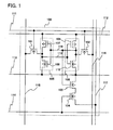
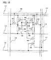
- An initialization memory cell 100 includes a first inverter circuit 105 having a first transistor 107 and a second transistor 108, a second inverter circuit 106 having a third transistor 109 and a fourth transistor 110, a fifth transistor 101, a sixth transistor 102, a seventh transistor 103, an eighth transistor 104, a power supply line 112, a ground line 113, a word line 111 which is to be a first word line, a word line 114 which is to be a second word line, a first data line (for writing) 115, a second data line (for writing) 116, and a third data line (for reading) 117.
- the second transistor 108, the fourth transistor 110, the fifth transistor 101, the sixth transistor 102, the seventh transistor 103, and the eighth transistor 104 are n-channel transistors.
- the first transistor 107 and the third transistor 109 are p-channel transistors.
- a first terminal of the first transistor 107 is connected to the power supply line 112.
- a gate terminal of the second transistor 108 is connected to a gate terminal of the first transistor 107
- a first terminal of the second transistor 108 is connected to a second terminal of the first transistor 107
- a second terminal of the second transistor 108 is connected to the ground line 113.
- a connection portion of the gate terminal of the first transistor 107, the gate terminal of the second transistor 108, and another element is an input terminal of the first inverter circuit 105.
- the first terminal of the first transistor 107 is a first potential supply terminal of the first inverter circuit 105.
- the second terminal of the second transistor 108 is a second potential supply terminal of the first inverter circuit 105.
- a connection portion of the second terminal of the first transistor 107, the first terminal of the second transistor 108, and another element is an output terminal of the first inverter circuit 105.
- a first terminal of the third transistor 109 is connected to the power supply line 112.
- a gate terminal of the fourth transistor 110 is connected to a gate terminal of the third transistor 109.
- a first terminal of the fourth transistor 110 is connected to a second terminal of the third transistor 109.
- a second terminal of the fourth transistor 110 is connected to the ground line 113.
- a connection portion of the gate terminal of the third transistor 109, the gate terminal of the fourth transistor 110, and another element is an input terminal of the second inverter circuit 106.
- the first terminal of the third transistor 109 is a first potential supply terminal of the second inverter circuit 106.
- the second terminal of the fourth transistor 110 is a second potential supply terminal of the second inverter circuit 106.
- a connection portion of the second terminal of the third transistor 109, the first terminal of the fourth transistor 110, and another element is an output terminal of the second inverter circuit 106.
- the input terminal of the first inverter circuit 105 is connected to the output terminal of the second inverter circuit 106.
- the output terminal of the first inverter circuit 105 is connected to the input terminal of the second inverter circuit 106.
- a gate terminal of the fifth transistor 101 is connected to the word line 111.
- a first terminal of the fifth transistor 101 is connected to the first data line 115.
- a second terminal of the fifth transistor 101 is connected to the output terminal of the first inverter circuit 105.
- a gate terminal of the sixth transistor 102 is connected to the word line 111.
- a first terminal of the sixth transistor 102 is connected to the output terminal of the second inverter circuit 106.
- a second terminal of the sixth transistor 102 is connected to the second data line 116.
- a gate terminal of the seventh transistor 103 is connected to the input terminal of the first inverter circuit 105 and the output terminal of the second inverter circuit 106.
- a first terminal of the seventh transistor 103 is connected to the ground line 113.
- a connection portion of the gate terminal of the seventh transistor 103, the input terminal of the first inverter circuit 105, and the output terminal of the second inverter circuit 106 is a first node 118.
- a connection portion of the output terminal of the first inverter circuit 105 and the input terminal of the second inverter circuit 106 is a second node 119.
- a gate terminal of the eighth transistor 104 is connected to the word line 114.
- a first terminal of the eighth transistor 104 is connected to a second terminal of the seventh transistor 103.
- a second terminal of the eighth transistor 104 is connected to the third data line 117.
- Normal data of writing data is input to the first data line 115 and an inverted data of the writing data is input to the second data line 116. That is, when the writing data is 1, data of 1 is input to the first data line 115 and data of 0 is input to the second data line 116. When the writing data is 0, data of 0 is input to the first data line 115 and data of 1 is input to the second data line 116.
- the third data line 117 is precharged with 3 V by a writing/reading circuit except during data is being read out.
- the wiring/reading circuit has functions of outputting writing data to the initialization memory cell 100 through the first data line 115 and the second data line 116 and reading out data in a memory cell from a potential of the third data line 117. In the case where a plurality of initialization memory cells is arranged in a line, at least one writing/reading circuit is provided for the memory cells in one line.
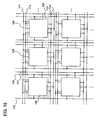
- FIG. 16 illustrates the structure of the semiconductor memory device in this embodiment.
- the semiconductor memory device in this embodiment includes a plurality of memory cell groups 125 each including the initialization memory cell 100 and a data hold memory cell 124 which has a function of holding data, a plurality of data lines 115, a plurality of second data lines 116, a plurality of third data lines 117, a plurality of word lines 111, a plurality of word lines 114, a plurality of power supply lines 112, and a plurality of ground lines 113.
- Each of the plurality of memory cell groups 125 is connected to the first data line 115, the second data line 116, the third data line 117, the word line 111, the word line 114, the power supply line 112, and the ground line 113.
- the structure shown in FIG 1 can be applied.
- the structure shown in FIG. 1 can be applied.
- 3 V is held in the word line 111 and data is written in the initialization memory cell 100 when the fifth transistor 101 and the sixth transistor 102 are turned on.
- 3 V is held in the word line 114 and the eighth transistor 104 is turned on.
- a potential of the first node 118 is 3 V (a potential of the second node 119 is 0 V) and the eighth transistor 104 is turned on, a potential of the third data line 117 which is precharged is made to be 0 V by the seventh transistor 103 and the eighth transistor 104.
- the potential of the third data line 117 which is precharged is kept at 3 V because the potential of the first node 118 is 0 V (the potential of the second node 119 is 3 V) and the seventh transistor 103 is off.
- the data in the initialization memory cell 100 is held by the first inverter circuit 105 and the second inverter circuit 106.
- a reverse case the case where the data in the initialization memory cell 100 is 0
- the memory cell cannot hold the data because the first inverter circuit 105 and the second inverter circuit 106 do not operate.
- the potential of the first node 118 cannot be identified unless given data is written in the initialization memory cell 100 at least once because the potential of the first node 118 is determined by factors such as a difference between input/output characteristics of the first inverter circuit 105 and the second inverter circuit 106, and wiring capacitance of the first node 118 and the second node 119.
- the initialization memory cell in this embodiment, differences between rising characteristics and between falling characteristics of the first inverter circuit 105 and the second inverter circuit 106 with respect to an input signal are made.
- the initialization memory cell which is connected to each word line holds data of 1 when the data stored in the memory cell is valid, and hold data of 0 when the data stored in the memory cell is invalid. Since whether each word line is valid or invalid can be set at will in accordance with a circuit configuration, a reverse case is also possible.
- data of 0 is held in the initialization memory cell, and the potential of the first node 118 is 3 V and the potential of the second node 119 is 0 V.
- the first inverter circuit 105 and the second inverter circuit 106 do not operate.
- the potentials of the first node 118 and the second node 119 are 0 V.
- the first inverter circuit 105 and the second inverter circuit 106 start operating.
- the potential of the first node 118 is input to the first inverter circuit 105 and the first inverter circuit 105 outputs a potential of the power supply line 112 (also referred to as a power supply potential) or a potential of the ground line 113 (also referred to as a ground potential) to the second node 119.
- the potential of the second node 119 is input to the second inverter circuit 106 and the second inverter circuit 106 outputs the power supply potential or the ground potential to the first node 118.
- the potential of the first node 118 is determined in accordance with a difference between input/output characteristics of the two inverter circuits.
- two inverter circuits whose transistors have the same size are provided in order to make output current characteristics of the two inverter circuits with respect to an input voltage to be the same with a balance so that writing operation and reading operation can be stably performed by the memory cell.
- the size of the transistors are determined by a channel length and a channel width.
- the differences are made at will between the rising characteristics and between the falling characteristics of the first inverter circuit 105 and the second inverter circuit 106 with respect to an input signal so that data to be held in the initialization memory cell is determined.
- the rising characteristic of the third transistor 109 in the second inverter circuit 106 is set to be better than that of the first transistor 107 in the first inverter circuit 105; that is, an absolute value of a threshold voltage of the third transistor 109 is made smaller than that of the first transistor 107.
- the third transistor 109 is turned on faster than the first transistor 107 and can output a larger amount of current, and therefore, the potential of the first node 118 can be 3 V
- the potential of the second node 119 is determined to be 0 V by the n-channel transistor in the first inverter circuit 105. In this manner, since the data in the initialization memory cell is made to be 0, initialization processing can be performed at the same time as the power supply is turned on.
- the rising characteristic of the second transistor 108 in the first inverter circuit 105 is made better than that of the fourth transistor 110 in the second inverter circuit 106, that is, the absolute value of a threshold voltage of the second transistor 108 may be made smaller than that of the fourth transistor 110.
- the potential of the first node which is changed from 0 V to 3 V, is input to the second transistor 108 immediately after the power supply is turned on. If a rising characteristic of a transistor is good, the transistor is turned on faster and can output a large amount of current.
- the potential of the second node 119 which is being increased to 3 V by the first transistor 107, can be lowered to 0 V
- initialization processing can be performed at the same time as the power supply is turned on.
- a structure in which the fifth transistor 101, the sixth transistor 102, the seventh transistor 103, and the eighth transistor 104 are p-channel transistors can be employed.
- initialization processing can be performed at the same time as the power supply is turned on in a similar manner, by setting a potential applied to each terminal to an opposite value to a potential applied to each terminal shown in FIG 1 . Further, at that time, the third data line 117 is not necessary to be precharged.
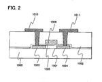
- the transistor includes a semiconductor layer 1001 provided over a substrate 1000, a gate insulating layer 1005 provided over the semiconductor layer 1001, a gate electrode 1006 provided over the gate insulating layer 1005, an insulating layer 1002 provided over the gate electrode 1006, and a first wiring 1010 and a second wiring 1011 formed over the semiconductor layer 1001 through contact portions provided in the insulating layer 1002.
- the semiconductor layer 1001 includes a first impurity region 1003 and a second impurity region 1004 to which impurity elements are added.
- a glass substrate a quartz substrate, a metal substrate (e.g., a stainless-steel substrate), a ceramics substrate, or the like can be used.
- a plastic substrate can also be used.
- a substrate made of polyethylene terephthalate (PET), polyethylene naphthalate (PEN), polyethersulfone (PES), acrylic, or the like can be used.
- the gate insulating layer 1005 and the insulating layer 1002 each can be formed of any one or a plurality of silicon oxide, silicon nitride, silicon oxynitride, and silicon nitride oxide. Further, the gate insulating layer 1005 and the insulating layer 1002 each can be formed with a stacked-layer structure of selected materials from the above mentioned materials. The gate insulating layer 1005 and the insulating layer 1002 can be formed by CVD, sputtering, or the like.
- the semiconductor layer 1001 can be formed of amorphous silicon, polycrystalline silicon, microcrystalline silicon (also referred to as semi-amorphous silicon), or the like: Furthermore, the semiconductor layer 1001 can be formed by sputtering, LPCVD, plasma CVD, or the like.
- the semiconductor layer 1001 is irradiated with a laser beam to be crystallized.
- the semiconductor layer 1001 can also be crystallized by a method in which laser beam irradiation, thermal crystallization using RTA or an annealing furnace, and thermal crystallization using a metal element which promotes crystallization are combined, or the like. After that, the obtained crystalline semiconductor film is etched into a desired shape so that the semiconductor layer 1001 is formed.
- a laser beam used for crystallization either a continuous wave laser (a CW laser) or a pulsed laser can be used.
- a laser beam that can be used here one or more of laser beams emitted from the followings can be given: a gas laser such as an Ar laser, a Kr laser, or an excimer laser; a laser whose medium is a single-crystal YAG, YVO 4 , forsterite (Mg 2 SiO 4 ), YAlO 3 , or GdVO 4 or a polycrystalline (ceramic) YAG, Y 2 O 3 , YVO 4 , YAlO 3 , or GdVO 4 , each of which is doped with one or more of Nd, Yb, Cr, Ti, Ho, Er, Tm, and Ta; a glass laser; a ruby laser; an alexandrite laser; a Ti:sapphire laser; a copper vapor laser; and a gold vapor laser.
- a gas laser such
- crystals with a large grain size can be obtained.
- the second harmonic (532 nm) or the third harmonic (355 nm) of an Nd:YVO 4 laser (fundamental wave of 1064 nm) can be used.
- a laser power density of about greater than or equal to 0.01 MW/cm 2 and less than or equal to 100 MW/cm 2 (preferably, greater than or equal to 0.1 MW/cm 2 and less than or equal to 10 MW/cm 2 ) is required, and irradiation is conducted with a scanning rate of about greater than or equal to 10 cm/sec and less than or equal to 2000 cm/sec.
- a laser whose medium is a single-crystal YAG, YVO 4 , forsterite (Mg 2 SiO 4 ), YAlO 3 , or GdVO 4 or a polycrystalline (ceramic) YAG, Y 2 O 3 , YVO 4 , YAlO 3 , or GdVO 4 , each of which is doped with one or more of Nd, Yb, Cr, Ti, Ho, Er, Tm, and Ta; an Ar ion laser; or a Ti:sapphire laser can function as a CW laser and can also function as a pulsed laser with a repetition rate of 10 MHz or higher by mode locking.
- a laser beam is oscillated with a repetition rate of 10 MHz or higher
- a semiconductor film is irradiated with a pulsed laser beam after the semiconductor layer is melted by the previous laser beam and before the melted semiconductor film is solidified. Therefore, unlike a pulsed laser with low repetition rate, an interface between a solid phase and a liquid phase can be moved continuously in the semiconductor layer, whereby crystal grains grown continuously toward a direction where the laser beam is moved can be obtained
- a method in which thermal treatment is performed on an amorphous semiconductor layer can also be employed.
- a heating furnace is used for the thermal treatment, an amorphous silicon layer is heated at 400 to 550 °C for 2 to 20 hours.
- a metal which promotes crystallization of a semiconductor layer such as nickel
- a solution containing nickel is applied to the amorphous silicon layer and thermal treatment is performed thereon, whereby a heating temperature can be lowered and a polycrystalline silicon layer having a continuous grain boundary can be obtained.
- the metal which promotes crystallization iron, ruthenium, rhodium, palladium, osmium, iridium, platinum, copper, or the like can be used as well as nickel.
- a gettering step for removing metal is preferably performed after the amorphous silicon layer is crystallized.
- a layer which is to be a gettering sink is formed over the silicon layer, and the silicon layer is heated so that the metal is moved into the gettering sink when the silicon layer is heated.
- the gettering sink a polycrystalline semiconductor layer or a semiconductor layer to which impurities are added can be used.
- a polycrystalline silicon layer to which an inert element such as argon is added is formed over the silicon layer to be used as the gettering sink.
- the metal can be captured more efficiently.
- the metal can be captured by addition of an element such as phosphorus to part of the semiconductor layer in the transistor, without forming the gettering sink.
- the gate electrode 1006 can be formed by using an element selected from tantalum, tungsten, titanium, molybdenum, aluminum, copper, chromium, niobium, or the like, or an alloy material or compound material containing any of the elements as its main component.
- a semiconductor material typified by polycrystalline silicon which is doped with an impurity element such as phosphorus can be used.
- a stacked-layer structure of one or a plurality of materials selected from those listed above can also be employed.
- Examples of a combination of the materials listed above includes a tantalum nitride film and a tungsten film, a tungsten nitride film and a tungsten film, a molybdenum nitride film and a molybdenum film, and the like. Since tungsten and tantalum nitride have high heat resistance, thermal treatment for thermal activation can be performed after a first layer and a second layer of the gate electrode are formed. Alternatively, not only a two-layer structure but also a three-layer structure can be employed. In the case of the three-layer structure, for example, a stacked-layer structure of a molybdenum film, an aluminum film, and a molybdenum film can be employed.
- the first impurity region 1003 and the second impurity region 1004 can be formed by adding an impurity element to part of the semiconductor layer 1001. If the impurity element is desired to be added to a predetermined region, a resist is formed and the impurity element is added using the resist as a mask, whereby each of the first impurity region 1003 and the second impurity region 1004 containing a desired element in a desired region can be formed.
- the impurity element phosphorus or boron can be used as the impurity element.
- an inorganic material such as oxide of silicon or nitride of silicon
- an organic material such as polyimide, polyamide, benzocyclobutene, acrylic, or epoxy
- a siloxane material can be used as the insulating layer 1002
- an inorganic material such as oxide of silicon or nitride of silicon
- an organic material such as polyimide, polyamide, benzocyclobutene, acrylic, or epoxy
- a siloxane material can be used as a stacked-layer structure of one or a plurality of materials selected from those listed above can also be employed.
- Each of the first wiring 1010 and the second wiring 1011 functions as a source wiring and a drain wiring, and each can be formed from an element selected from aluminum, tungsten, titanium, tantalum, molybdenum, nickel, platinum, copper, gold, silver, manganese, neodymium, carbon, or silicon, or an alloy material or compound material containing any of the elements as its main component listed above. Further, a stacked-layer structure of one or a plurality of materials selected from those listed above can also be employed.
- an alloy material containing aluminum as its main component for example, a material containing aluminum as its main component and also nickel, or an alloy material containing aluminum as its main component, nickel, and one or both of carbon and silicon, or the like can be used.
- the first wiring 1010 and the second wiring 1011 may employ, for example, a stacked layer structure of a barrier film, an aluminum-silicon (Al-Si) film, and a barrier film, or a stacked layer structure of a barrier film, an aluminum-silicon (Al-Si) film, a titanium nitride film, and a barrier film.
- a barrier film corresponds to a thin film formed by using titanium, a nitride of titanium, molybdenum, or a nitride of molybdenum.
- Aluminum and aluminum silicon which have low resistance and are inexpensive are optimal materials for forming the first wiring 1010 and the second wiring 1011.
- the barrier film is formed by using titanium that is a highly-reducible element, even if a thin natural oxide film is formed over the crystalline semiconductor film, the natural oxide film can be reduced so that preferable contact with the crystalline semiconductor film can be obtained.
- Either the first impurity region 1003 and the first wiring 1010, or the second impurity region 1004 and the second wiring 1011 functions as either a source terminal or a drain terminal.
- a channel-forming region is formed between the first impurity region 1003 and the second impurity region 1004.
- a staggered transistor is illustrated in this embodiment mode, the present invention is not limited thereto.
- An inversely staggered transistor can also be employed.
- a transistor a transistor using a single-crystal semiconductor film can be used.
- the transistor using a single crystal is shown in FIG 3 .
- the transistor using a single crystal includes a substrate 2011 which is formed of silicon or the like, an insulating layer 2012, a semiconductor substrate 2000, a gate insulating layer 2006 formed over the semiconductor substrate 2000, and a gate electrode 2007 formed over the gate insulating layer 2006.
- the semiconductor substrate 2000 includes a first insulating layer 2004, a second insulating layer 2005, and a well region 2001.
- the well region 2001 includes a first impurity region 2002 and a second impurity region 2003.
- the gate insulating layer 2006 and the gate electrode 2007 are formed over a region between the first impurity region 2002 and the second impurity region 2003 in the semiconductor substrate 2000.
- an insulating layer 2008 is formed over the gate electrode 2007 and the semiconductor substrate 2000.
- the given number of contact portions are provided in parts of the insulating layer 2008, and a first wiring 2009 and a second wiring 2009 are formed over the first impurity region 2002 and the second impurity region 2003, respectively, through the contact portions.
- a single-crystal silicon substrate having a n-type or p-type conductivity or a compound semiconductor substrate (a GaAs substrate, an InP substrate, a GaN substrate, an SiC substrate, a sapphire substrate, a ZnSe substrate, or the like) can be used.
- a selective oxidation method (a LOCOS (local oxidation of silicon) method), a trench isolation method, or the like can be used.
- the gate electrode 2007 tantalum, tungsten, titanium, molybdenum, aluminum, copper, chromium, niobium, or the like can be used.
- the gate electrode 2007 can be formed using a film formed of an alloy or a compound containing any of the metals as its main component can be used.
- the gate electrode 2007 can be formed of a semiconductor such as polycrystalline silicon doped with an impurity element which imparts a conductivity type to a semiconductor film, such as phosphorus. Further, the gate electrode 2007 can be formed by being patterned (patterning or the like) into a predetermined shape.
- the well region 2001, the first impurity region 2002, and the second impurity region 2003 can be formed by addition of an impurity element.
- an impurity element an impurity element imparting n-type or p-type conductivity is used.
- an impurity element imparting n-type conductivity phosphorus, arsenic, or the like can be used.
- an impurity element imparting p-type conductivity boron, aluminum, gallium, or the like can be used.
- the impurity element is desired to be added to a predetermined region, a resist is formed and the impurity element is added using the resist as a mask, whereby the well region 2001, the first impurity region 2002, and the second impurity region 2003 each containing a desired element can be formed in the predetermined regions.
- the gate insulating layer 2006 can be formed using an inorganic material, an organic material, or a mixed material of an organic material and an inorganic material.
- a film containing silicon oxide, silicon oxynitride, silicon nitride oxide, or carbon typified by DLC (diamond like carbon), acrylic, epoxy, polyimide, polyamide, polyvinylphenol, benzocyclobutene, or the like can be used.
- the first insulating layer 2004 and the second insulating layer 2005 can be formed by a CVD method, a sputtering method, a droplet discharging method, or a printing method in accordance with a material thereof.
- a channel-forming region is formed between the first impurity region 2002 and the second impurity region 2003.
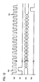
- a relationship between the thickness of a semiconductor layer and a rising characteristic of a transistor has been generally said as follows.
- Transistors have short-channel effect in which a threshold voltage is decreased when a channel length is shortened.
- a method for suppressing the short-channel effect a method in which the thickness of the semiconductor layer is reduced can be given.
- a semiconductor layer which is quarter to half the channel length in thickness is necessary in order to suppress the short-channel effect.
- the transistor can be employed by further reducing the thickness of another transistor beyond the above-described range of the thickness to make the other transistor have a thickness which prevents short-channel effect more certainly.
- a relationship between a film thickness and a threshold voltage of an n-channel transistor is shown in FIG 4 .
- a horizontal axis represents a voltage Vg between a gate terminal and a source terminal and a vertical axis represents a current I d which flows between a drain terminal and the source terminal.
- a characteristic curve 800 in the case where the thickness of the semiconductor layer is within a range of causing short-channel effect shows a decrease in the threshold voltage.
- Vg 0 V
- the threshold voltage can be further decreased by adjusting the dope amount of an impurity element in a channel portion so that a current consumption can be reduced.
- the rising characteristics of the transistor can be changed by changing the thickness of the semiconductor layer. Therefore, in this embodiment , differences between rising characteristics and between falling characteristics of one transistor in the first inverter circuit 105 and one transistor in the second inverter circuit 106, having conductivity which is the same as that of the one transistor in the first inverter circuit 105 can be made by changing the thicknesses of the semiconductor layers of the transistors which are to have the differences from each other.
- the rising characteristics of transistors can be different from each other. Specifically, the rising characteristic of the transistor is improved when the thickness of the gate insulating film is made thinner. For example, rising characteristics and falling characteristics of one transistor in the first inverter circuit 105 and one transistor in the second inverter circuit 106 which has the same conductivity as that of the one transistor in the first inverter circuit 105 could be made different from each other when the gate insulating layer of the one transistor in the second inverter circuit 106 made thinner than that of the one transistor in the first inverter circuit 105.
- each of the memory cell groups 125 also referred to as a memory line
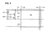
- the initialization memory cell 100 shown in FIG 1 includes the initialization memory cell 100 shown in FIG 1 and the data hold memory cell 124, in order to control the potentials of the first node 118 and the second node 119 at the time when power supply is turned from L to H and to perform initialization process more certainly.
- the structure of the initialization memory cell in FIG 5 includes the initialization memory cell 100 shown in FIG 1 , a ninth transistor 120, a resistor element 121, and a capacitor element 122.
- a gate terminal of the ninth transistor 120 is connected to the power supply line 112 through the resistor element 121 and to the ground line 113 through the capacitor element 122, a first terminal of the ninth transistor 120 is connected to the word line 111, and a second terminal of the ninth transistor 120 is connected to the ground line 113.
- a connecting wiring of the gate terminal of the ninth transistor 120, the resistor element 121, and the capacitor element 122 is a wiring 123. Note that the ninth transistor 120 is a p-channel transistor.
- a clock signal is denoted by a signal 300
- a power supply voltage is denoted by a power supply voltage 301
- a reset signal is denoted by a signal 302
- a signal of the wiring 123 is denoted by a signal 303
- an access signal from outside such as a CPU is denoted by a signal 304.
- the signal 303 When the power supply is turned on, the signal 303 is turned from L to H at the same time, held in that state for a certain period, and turned to L thereafter. Each circuit performs reset operation while the signal 302 is H.
- the signal 303 is turned from L to H a little later than turning-on of the power supply.
- Amount of the resistor element 121 and the capacitor element 122 can determine how long the signal 303 is to be delayed from turning-on of the power supply. Since a potential of the word line 111 changes from a ground potential to another potential when the signal 303 is turned from L to H, the signal 303 may be set to be turned from L to H during a reset operation period. After the signal 302 is turned to L, the reset operation is over at an event timing 401 in the signal 300 and a pulse of the signal 304 is input so that access to an external circuit starts.
- the structure makes it possible for all the initialization memory cells to perform invalidation process more certainly at the same time as power supply is turned on. Therefore, data can be initialized at higher speed.
- the structure shown in FIG 15 can also perform similar operation by connecting the first terminal of the ninth transistor 120 to the power supply line 112 in the circuit configuration shown in FIG 5 .
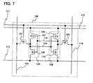
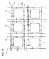
- the structure shown in FIG 7 does not include the third data line 117, the word line 114, the seventh transistor 103, and the eighth transistor 104.
- FIG 17 illustrates a case where the structure of the memory cell shown in FIG 7 is applied to the semiconductor device in this embodiment.
- the semiconductor memory device in this embodiment includes the plurality of memory cell groups 125 including the initialization memory cell 100 and the data hold memory cell 124 which has a function of holding data, the plurality of first data lines 115, the plurality of second data lines 116, the plurality of third data lines 117, the plurality of word lines 111, the plurality of power supply lines 112, and the plurality of ground lines 113
- Each memory cell in the plurality of memory cell groups 125 is connected to the first data line 115, the second data line 116, the third data line 117, the word line 111, the power supply line 112, and the ground line 113.
- the initialization memory cell 100 for example, the structure shown in FIG 7 can be applied.
- the structure shown in FIG 7 can be applied.
- circuit configurations of the initialization memory cell and the data hold memory cell can be different from each other.
- one of the initialization memory cell and the data hold memory cell may have the circuit configuration shown in FIG 1
- the other thereof may have the circuit configuration shown in FIG 7 .
- the area of the memory cell can be smaller than that of the memory cell in FIG 1 .
- the structure shown in FIG 7 can be applied to the memory cell 124 in FIG 16 .
- data writing operation is performed in the same manner as in FIG 1 , though data reading operation is performed in a different manner.
- the reading operation will be specifically described.
- 3 V is held in the word line 111, and the fifth transistor 101 and the sixth transistor 102 are turned on.
- a potential of the first data line 115 becomes the same as that of the second node 119, and a potential of the second data line 116 becomes the same as that of the first node 118.
- the writing/reading circuit detects the potentials of the first node 118 and the second node 119.
- the potential of the first node 118 is 3 V (the potential of the second node 119 is 0 V)
- the potential of the second data line 116 is 3 V (the potential of the first data line 115 is 0 V).
- the potential of the first node 118 is 0 V (the potential of the second node 119 is 3 V)
- the potential of the second data line 116 is 0 V (the potential of the first data line 115 is 3 V).
- a rising characteristic of the first transistor 107 in the first inverter circuit 105 is improved, that is, the first transistor 107 is turned on faster. Further, by improving a rising characteristic of the fourth transistor 110 in the second inverter circuit 106, initialization processing can be automatically performed at the same time as power supply is turned on.
- initialization of data in initialization processing in each memory cell can be performed at high speed.
- FIG 8 A structure of an initialization memory cell in a semiconductor memory device of this first example is shown in FIG 8 .
- a memory cell 200 for initialization processing includes a first inverter circuit 205 having a first transistor 207 and a second transistor 208, a second inverter circuit 206 having a third transistor 209 and a fourth transistor 210, a fifth transistor 201, a sixth transistor 202, a seventh transistor 203, an eighth transistor 204, a power supply line 212, a ground line 213, a word line 211 which is to be a first word line, a word line 214 which is to be a second word line, a first data line 215, a second data line 216, a third data line 217, and a bias circuit 220.
- the second transistor 208, the fourth transistor 210, the fifth transistor 201, the sixth transistor 202, the seventh transistor 203, and the eighth transistor 204 are n-channel transistors. Further, the first transistor 207 and the third transistor 209 are p-channel transistors.
- a first terminal of the first transistor 207 is connected to the power supply line 212.
- a gate terminal of the second transistor 208 is connected to a gate terminal of the first transistor 207, a first terminal of the second transistor 208 is connected to a second terminal of the first transistor 207, and a second terminal of the second transistor 208 is connected to the ground line 213.
- a connection portion of the gate terminal of the first transistor 207, the gate terminal of the second transistor 208, and another element is an input terminal of the first inverter circuit 205.
- the first terminal of the first transistor 207 is a first potential supply terminal of the first inverter circuit 205.
- the second terminal of the second transistor 208 is a second potential supply terminal of the first inverter circuit 205.
- a connection portion of the second terminal of the first transistor 207, the first terminal of the second transistor 208, and another element is an output terminal of the first inverter circuit 205.
- a first terminal of the third transistor 209 is connected to the power supply line 212.
- a gate terminal of the fourth transistor 210 is connected to a gate terminal of the third transistor 209.
- a first terminal of the fourth transistor 210 is connected to a second terminal of the third transistor 209.
- a second terminal of the fourth transistor 210 is connected to the ground line 213.
- a connection portion of the gate terminal of the third transistor 209, the gate terminal of the fourth transistor 210, and another element is an input terminal of the second inverter circuit 206.
- the first terminal of the third transistor 209 is a first potential supply terminal of the second inverter circuit 206.
- the second terminal of the fourth transistor 210 is a second potential supply terminal of the second inverter circuit 206.
- a connection portion between the second terminal of the third transistor 209 and the first terminal of the fourth transistor 210 is an output terminal of the second inverter circuit 206.
- the input terminal of the first inverter circuit 205 is connected to the output terminal of the second inverter circuit 206.
- the output terminal of the first inverter circuit 205 is connected to the input terminal of the second inverter circuit 206.
- a gate terminal of the fifth transistor 201 is connected to the word line 211.
- a first terminal of the fifth transistor 201 is connected to the first data line 215.
- a second terminal of the fifth transistor 201 is connected to the output terminal of the first inverter circuit 205.
- a gate terminal of the sixth transistor 202 is connected to the word line 211.
- a first terminal of the sixth transistor 202 is connected to the output terminal of the second inverter circuit 206.
- a second terminal of the sixth transistor 202 is connected to the second data line 216.
- a gate terminal of the seventh transistor 203 is connected to the input terminal of the first inverter circuit 205 and the output terminal of the second inverter circuit 206.
- a first terminal of the seventh transistor 203 is connected to the ground line 213.
- a connection portion of the gate terminal of the seventh transistor 203, the input terminal of the first inverter circuit 205, and the second inverter circuit 206 is a first node 218.
- a connection portion of the output terminal of the first inverter circuit 205 and the input terminal of the second inverter circuit 206 is a second node 219.
- a gate terminal of the eighth transistor 204 is connected to the word line 214.
- a first terminal of the eighth transistor 204 is connected to a second terminal of the seventh transistor 203.
- a second terminal of the eighth transistor 204 is connected to the third data line 217.
- Normal data of writing data is input to the first data line 215 and an inverted data of the writing data is input to the second data line 216.
- the third data line 217 is precharged with 3 V by a writing/reading circuit except during data is being read out.
- the writing/reading circuit has functions of outputting writing data to a memory cell through the first data line 215 and the second data line 216 and reading out data in a memory cell from a potential of the third data line 217.
- at least one writing/reading circuit corresponding thereto is provided.
- the initialization memory cell in FIG 8 includes the bias circuit 220.
- the bias circuit 220 is connected to a substrate terminal of the first transistor 207.
- the first transistor 207 a transistor in which a first gate terminal and a second gate terminal are provided with an active layer interposed therebetween can be used for example.
- a first voltage is applied to the active layer from the first gate terminal and a second voltage is applied to the active layer from the second gate terminal.
- a threshold voltage of the transistor can be controlled by controlling voltage values of the first voltage and the second voltage applied to the active layer.
- one of the first gate terminal and the second gate terminal is referred to as a substrate terminal, and a voltage applied to the substrate terminal is referred to as a substrate voltage in some cases.
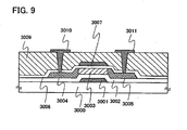
- a transistor shown in FIG. 9 includes a substrate 3000, a first gate electrode 3001 provided over the substrate 3000, a first gate insulating layer 3002 provided over the first gate electrode 3001, a semiconductor layer 3003 provided over the first gate insulating layer 3002, a second gate insulating layer 3006 provided over the semiconductor layer 3003, and a second gate electrode 3007 provided over the second gate insulating layer 3006.
- the semiconductor layer 3003 includes a first impurity region 3004 and a second impurity region 3005.
- An insulating layer 3009 is formed over the second gate electrode 3007.
- the given number of contact portions are provided in parts of the insulating layer 3009, and a first wiring 3010 and a second wiring 3011 are formed over the first impurity region 3004 and the second impurity region 3005, respectively, through the contact portions.
- a glass substrate As the substrate 3000, a glass substrate, a quartz substrate, a metal substrate (e.g., a stainless-steel substrate), a ceramics substrate, or the like can be used.
- a plastic substrate made of polyethylene terephthalate (PET), polyethylene naphthalate (PEN), polyethersulfone (PES), acrylic, or the like can be used.
- the first gate insulating layer 3002, the second gate insulating layer 3006, and the insulating layer 3009 each can be formed of any one of or a plurality of silicon oxide, silicon nitride, silicon oxynitride, and silicon nitride oxide. Further, the first gate insulating layer 3002, the second gate insulating layer 3006, and the insulating layer 3009 each can be formed with a stacked-layer structure of selected materials from the above mentioned materials. The first gate insulating layer 3002, the second gate insulating layer 3006, and the insulating layer 3009 can be formed by CVD, sputtering, or the like.
- the semiconductor layer 3003 can be formed of amorphous silicon, polycrystalline silicon, microcrystalline silicon (also referred to as semi-amorphous silicon), or the like. Furthermore, the semiconductor layer 3003 can be formed by sputtering, LPCVD, plasma CVD, or the like.
- the semiconductor layer 3003 is irradiated with a laser beam to be crystallized.
- the semiconductor layer 3003 can also be crystallized by a method in which laser beam irradiation, thermal crystallization using RTA or an annealing furnace, and thermal crystallization using a metal element which promotes crystallization are combined, or the like. After that, the obtained crystalline semiconductor film is etched into a desired shape so that the semiconductor layer 3003 is formed.
- a laser beam similar to the laser beam which can be employed for the semiconductor layer in the Embodiment of the invention can be used.
- the first gate electrode 3001 and the second gate electrode 3007 each can be formed by using an element selected from tantalum, tungsten, titanium, molybdenum, aluminum, copper, chromium, niobium, or the like, or an alloy material or compound material containing any of the elements as its main component.
- a semiconductor material typified by polycrystalline silicon which is doped with an impurity element such as phosphorus can be used.
- a stacked-layer structure of one or a plurality of elements selected from those listed above can be employed.
- Examples of a combination of the elements listed above includes: a tantalum nitride film and a tungsten film, a tungsten nitride film and a tungsten film, a molybdenum nitride film and a molybdenum film, and the like. Since tungsten and tantalum nitride have high heat resistance, thermal treatment for thermal activation can be performed after a first layer and a second layer of the gate electrode are formed. Alternatively, not only a two-layer structure but also a three-layer structure can be employed. In the case of the three-layer structure, for example, a stacked-layer structure of a molybdenum film, an aluminum film, and a molybdenum film can be employed.
- the first impurity region 3004 and the second impurity region 3005 each can be formed by adding an impurity element to part of the semiconductor layer 3003. If the impurity element is desired to be added to predetermined regions, a resist is formed and the impurity element is added using the resist as a mask, whereby each of the first impurity region 3004 and the second impurity region 3005 containing a desired element in a desired region can be formed.
- the impurity element phosphorus or boron can be used as the impurity element.
- an inorganic material such as oxide of silicon or nitride of silicon
- an organic material such as polyimide, polyamide, benzocyclobutene, acrylic, or epoxy
- a siloxane material can be used as the insulating layer 3009.
- a stacked-layer structure of one or a plurality of materials selected from those listed above can also be employed.
- the first wiring 3010 and the second wiring 3011 each function as a source wiring and a drain wiring, and each can be formed from an element selected from aluminum, tungsten, titanium, tantalum, molybdenum, nickel, platinum, copper, gold, silver, manganese, neodymium, carbon, or silicon, or an alloy material or compound material containing any of the elements listed above. Further, a stacked-layer structure of one or a plurality of elements selected from those listed above can also be employed.
- an alloy material containing aluminum as its main component for example, a material containing aluminum as its main component and also nickel, or an alloy material containing aluminum as its main component, nickel, and one or both of carbon and silicon, or the like can be used.
- the first wiring 3010 and the second wiring 3011 each may employ, for example, a stacked-layer structure of a barrier film, an aluminum-silicon (Al-Si) film, and a barrier film, or a stacked-layer structure of a barrier film, an aluminum-silicon (Al-Si) film, a titanium nitride film, and a barrier film.
- a barrier film corresponds to a thin film made of titanium, a nitride of titanium, molybdenum, or a nitride of molybdenum.
- Aluminum and aluminum silicon which have low resistance and are inexpensive are optimal materials for forming the first wiring 3010 and the second wiring 3011.
- the barrier film is formed by using titanium that is a highly-reducible element, even if a thin natural oxide film is formed on the crystalline semiconductor film, the natural oxide film can be reduced so that preferable contact with the crystalline semiconductor film can be obtained.
- Either the first impurity region 3004 and the first wiring 3010, or the second impurity region 3005 and the second wiring 3011 functions as either a source terminal or a drain terminal.
- a channel-forming region is formed between the first impurity region 3004 and the second impurity region 3005.
- the first electrode 3001 or the second gate electrode 3007 functions as a substrate terminal (also referred to as a control terminal) in a transistor.
- a threshold voltage of the transistor can be controlled by application of a voltage to the channel-forming region from the bias circuit 220 in this first example through the first gate electrode 3001 or the second gate electrode 3007.
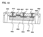
- a structure is shown in a cross-sectional view of a transistor having a single crystal semiconductor layer with reference to FIG 10 .
- a transistor shown in FIG 10 includes a substrate 4000, a gate insulating layer 4007 formed over the substrate 4000, a first insulating layer 4005, a second insulating layer 4006, and a gate electrode 4008 formed over the gate insulating layer 4007.
- Part of the substrate 4000 is a well region 4001.
- the well region 4001 includes a first impurity region 4002, a second impurity region 4003, and a third impurity region 4004.
- the gate insulating layer 4007 and the gate electrode 4008 are formed over a region between the first impurity region 4002 and the second impurity region 4003 in the substrate 4000. Further, an insulating layer 4009 is formed over the gate electrode 4008 and the substrate 4000.
- the given number of contact portions are provided in parts of the insulating layer 4009, and a first wiring 4010, a second wiring 4011, and a third wiring 4012 are formed over the first impurity region 4002, the second impurity region 4003, and the third impurity region 4004, respectively, through the contact portions.
- the first impurity region is a source region
- the second impurity region is a drain region
- the third impurity region is a region to which a voltage is applied.
- the first voltage is applied to the active layer from the gate electrode
- the second voltage is applied to the active layer from the third impurity region.
- a threshold voltage of the transistor can be controlled by controlling the voltage values of the first voltage and the second voltage applied to the active layer.
- the third impurity region is referred to as a substrate terminal and a voltage applied to the third impurity region is referred to as a substrate voltage in some cases.
- a single-crystal silicon substrate having a n-type or p-type conductivity, or a compound semiconductor substrate (a GaAs substrate, an InP substrate, a GaN substrate, an SiC substrate, a sapphire substrate, a ZnSe substrate, or the like) can be used.
- a selective oxidation method (a LOCOS (local oxidation of silicon) method), a trench isolation method, or the like can be used.
- the gate electrode 4008 can be formed of an element selected from tantalum, tungsten, titanium, molybdenum, aluminum, copper, chromium, niobium, or the like, or an alloy material or a compound material containing any of the elements as its main component.
- the gate electrode 4008 can be formed of a semiconductor such as polycrystalline silicon doped with an impurity element which imparts a conductivity to a semiconductor film, such as phosphorus.
- the gate electrode 4008 can be formed by being patterned (patterning or the like) into a predetermined shape.
- the well region 4001, the first impurity region 4002, the second impurity region 4003, and the third impurity region 4004 can be formed by addition of an impurity element.
- an impurity element imparting n-type or p-type conductivity is used.
- the impurity element imparting n-type conductivity phosphorus, arsenic, or the like can be used.
- As the impurity element imparting p-type conductivity boron, aluminum, gallium, or the like can be used.
- the impurity element is desired to be added to predetermined regions, a resist is formed and the impurity element is added using the resist as a mask, whereby the well region 4001, the first impurity region 4002, the second impurity region 4003, and the third impurity region 4004 containing a desired element in the predetermined region can be formed.
- the gate insulating layer 4007 can be formed using an inorganic material, an organic material, or a mixed material of an organic material and an inorganic material.
- a film containing silicon oxide, silicon oxynitride, silicon nitride oxide, or carbon typified by DLC (diamond like carbon), acrylic, epoxy, polyimide, polyamide, polyvinylphenol, benzocyclobutene, or the like can be used.
- the first insulating layer 4005 and the second insulating layer 4006 can be formed by a CVD method, a sputtering method, a droplet discharging method, or a printing method in accordance with a material thereof.
- Either the first impurity region 4002 and the first wiring 4010, or the second impurity region 4003 and the second wiring 4011 functions as either a source terminal or a drain terminal.
- a channel-forming region is formed between the first impurity region 4002 and the second impurity region 4003.
- the third impurity region 4004 and the third wiring 4012 function as a substrate terminal (also referred to as a control terminal) to which a voltage (a substrate voltage) different from a voltage applied to another terminal of the transistor.
- a threshold voltage of the transistor can be controlled by application of a voltage to the channel-forming region from the bias circuit 220 in FIG 8 through the third wiring 4012.
- the threshold voltage is changed so that rising characteristics and falling characteristics in the first inverter circuit 205 can be changed.
- Differences between rising characteristics and between falling characteristics of the first inverter circuit 205 and the second inverter circuit 206 with respect to an input signal are made so that data to be held in the initialization memory cell is determined corresponding thereto.
- a rising characteristic of the third transistor 209 in the second inverter circuit 206 is set to be better than that of the first transistor 207 in the first inverter circuit 205.
- the third transistor 209 can output larger amount of current faster than the first transistor 207 and therefore, the potential of the first node 218 can be 3 V
- the potential of the second node 219 is determined to be 0 V by the n-channel transistor in the first inverter circuit 205. In this manner, since the data in the memory cell is made to be 0, initialization processing can be performed at the same time as power supply is turned on.
- the potentials of the first node 218 and the second node 219 can be determined more quickly.
- the present invention is not limited thereto.
- a structure in which a transistor having a substrate terminal is applied to the second transistor 208 in the first inverter circuit 205, or the third transistor 209 or the fourth transistor 210 in the second inverter circuit 206, and the bias circuit 220 is connected to the substrate terminal of the transistor can be employed.
- a structure in which a plurality of bias circuits is used and a transistor having a substrate terminal is used as any of the second transistor 208 in the first inverter circuit 205, and the third transistor 209 and the fourth transistor 210 in the second inverter circuit 206 so that a plurality of transistors each is connected to one bias circuit can be employed.
- a threshold voltage of each transistor connected to the bias circuit can be controlled and differences between the rising characteristics and between falling characteristics of the first inverter circuit 205 and the second inverter circuit 206 can be made more obvious; and therefore, initialization processing can be performed more certainly at the same time as the power supply is turned on.
- initialization of data in initialization processing in each memory cell can be performed at high speed.
- a structure in which a conventional bias circuit is provided can be formed by the same steps as in the embodiment of the present invention.
- FIG. 11 A structure of a semiconductor device of this second example is shown in FIG. 11 .
- the semiconductor device shown in FIG 11 includes a CPU 906 and a main memory (also referred to as a second memory device) 901 which functions as a main memory device.
- the CPU 906 includes an arithmetic unit 900 and a cache memory (also referred to as a first memory device) 902 which functions as a subordinate memory device.
- the cache memory 902 includes a plurality of memory lines 903 which has a data memory 905 in which partial information of the arithmetic unit 900 is stored, a tag memory 904, and a valid bit 907.
- the tag memory 904 included in the cache memory 902 stores the data showing the address of the main memory 901 which has the source contents.
- the valid bit 907 has functions of showing whether the data stored in the cache memory 902 is valid or invalid and invalidating all the data stored in the cache memory 902 by initializing the valid bit 907 when power is supplied.
- the valid bit 907 is necessary to be invalidated at first so that the CPU does not use undefined data. Through this processing, access by the CPU 906 is judged as a cache miss and the undefined data is not to be used.
- each memory line 903 includes a valid bit of 1 bit, and holds data "0" when the memory line is valid, and holds data "1" when the memory line is invalid. This can be set as appropriate in accordance with a related circuit configuration; therefore, data showing whether the memory line is valid or invalid can be inverse of the above in some cases.
- the initialization memory cell 100 in the present invention differences are made between the rising characteristics and between the falling characteristics of two inverter circuits with respect to an input signal so that data to be held in the initialization memory cell 100 can be determined.
- the rising characteristic of a p-channel transistor in the second inverter circuit 106 is improved.
- the p-channel transistor in the second inverter circuit 106 is turned on faster than a p-channel transistor in the first inverter circuit 105 and can output larger amount of current, and therefore, the potential of the first node 118 can be 3 V
- the potential of the second node 119 is determined to be 0 V by the n-channel transistor in the first inverter circuit 105. In this manner, since the data in the initialization memory cell 100 is made to be 0, invalidation processing can be performed on the valid bit at the same time as the power supply is turned on.
- a rising characteristic of the n-channel transistor in the first inverter circuit 105 may be improved like as in the Embodiment of the invention or as in the first example 2.
- the potential of the first node 118 which changes from 0 V to 3 V, is input to the n-channel transistor in the first inverter circuit 105. If the rising characteristic is good, the transistor can be turned on much faster and output larger amount of current.
- the potential of the second node 119 which is increased to 3 V by the first transistor 107 in the first inverter circuit 105, can be decreased to 0 V Therefore, since the data in the initialization memory cell 100 can be made "0" more certainly, invalidation processing on the valid bit can be performed at the same time as the power supply is turned on.
- a rising characteristic of the p-channel transistor in the first inverter circuit 105 is improved. Further, a rising characteristic of the n-channel transistor in the second inverter circuit 106 is preferably improved.
- a potential of the word line 111 is made not to be 3 V because the potential of the second node 119 is made to be 0 V with certainty.
- a structure of the valid bit includes the initialization memory cell 100 shown in FIG 1 , the ninth transistor 120, the resistor element 121, and the capacitor element 122 shown in FIG 5 .
- a gate terminal of the ninth transistor 120 is connected to the power supply line 112 through the resistor element 121 and to the ground line 113 through the capacitor element 122.
- a first terminal of the ninth transistor 120 is connected to the word line 111, and a second terminal of the ninth transistor 120 is connected to the ground line 113.
- a connecting wiring of the gate terminal of the ninth transistor 120, the resistor element 121, and the capacitor element 122 is a wiring 123.
- the ninth transistor 120 is a p-channel transistor.
- a row decoder circuit has functions of selecting a memory cell for writing data by using the word line 111 and selecting a memory cell for reading data by using the word line 114. At least one row decoder circuit corresponding to the memory line is provided.
- the timing chart in FIG 6 can be employed for operation in the case where the memory cell shown in FIG 1 is applied to the valid bit in the cache memory of this embodiment and the circuit shown in FIG 5 is added to the row decoder as well.
- power supply is turned on and a power supply voltage is turned from L to H at an event timing 400 in the signal 300, all the memory cells are invalidated by the structure of the initialization memory cell shown in FIG 5 .
- the signal 303 is turned from L to H at the same time, held in that state for a certain period, and turned to L thereafter.
- Each circuit performs reset operation while the signal 302 is H.
- the signal 303 is turned from L to H a little later than turning-on of the power supply.
- Amount of the resistor element 121 and the capacitor element 122 can determine how long the signal 303 is to be delayed from turning-on of the power supply. Since a potential of the word line 111 changes from a ground potential to another potential when the signal 303 is turned from L to H, the signal 303 may be set to be turned from L to H during a reset operation period. After the signal 302 is turned to I, the reset operation is over at an event timing 401 in the signal 300 and a pulse of the signal 304 is input so that access to the cache memory starts.
- a first insulating layer 601 is formed over a substrate 600.
- the first insulating layer 601 can be formed with a single-layer or stacked-layer structure. In this embodiment, a two-layer structure is used for the first insulating layer 601.
- a silicon oxynitride layer having a thickness of 10 to 200 nm (preferably 50 to 100 nm) is formed.
- the silicon oxynitride layer can be formed by plasma CVD using SiH 4 , NH 3 , N 2 O, and H 2 as reactive gas.
- a silicon oxynitride layer having a thickness of 50 to 200 nm (preferably 100 to 150 nm) is formed.
- the silicon oxynitride layer can be formed by plasma CVD using SiH 4 , N 2 O, and the like as reactive gas. Note that as the substrate 600 and the first insulating layer 601, materials which can be employed for the substrate and the insulating layer of the transistor in the semiconductor memory device of Embodiment Mode 1 can be used.
- a semiconductor layer is formed over the first insulating layer 601.
- the semiconductor layer materials which can be employed for the semiconductor layer of the transistor in the semiconductor memory device of the Embodiment of the invention in fig. 2 or 3 can be used.
- the semiconductor layer may be an amorphous, crystalline, or microcrystalline semiconductor layer.
- a semiconductor layer having a crystalline structure such as a single crystalline or polycrystalline structure is preferably used because mobility of the transistor can be increased.
- the thus formed semiconductor layer is processed into a predetermined shape, thereby forming an island-shaped semiconductor layer.
- a first semiconductor layer 602 having a thickness of d1 and a second semiconductor layer 603 having a thickness of d2 which is greater than the thickness of d1 may be formed for example as shown in FIG 13A .
- etching using a mask formed by photolithography is performed. As etching, wet etching or dry etching can be employed.
- the first semiconductor layer 602 and the second semiconductor layer 603 are processed so as to have predetermined thicknesses different from each other.
- the semiconductor layer can be crystallized.
- a method for the crystallization a method which can be employed for the semiconductor layer of the transistor in the semiconductor memory device of the embodiment of the present invention of fig. 2 or 3 can be used.
- a gate insulating film 604 is formed so as to cover the first semiconductor layer 602 and the second semiconductor layer 603.
- materials which can be employed for the gate insulating layer of the transistor in the semiconductor memory device of the Embodiment of fig 2 or 3 can be used.
- first to third conductive layers 605 to 607 which function as a first gate electrode, a second electrode, and a gate wiring, respectively, are formed over the gate insulating film 604.
- the conductive layers are processed by etching using a mask that is formed by photolithography. As etching, wet etching or dry etching can be employed.
- materials which can be employed for the wiring of the transistor in the semiconductor memory device of the Embodiment of fig. 2 or 3 can be used.
- an impurity element is added to the first semiconductor layer 602 and the second semiconductor layer 603.
- phosphorus (P) may be used as the impurity element
- boron (B) may be used as the impurity element.
- impurity regions 608 to 611 are formed in the first semiconductor layer 602 and the second semiconductor layer 603.
- a high concentration impurity region and a low concentration impurity region can be formed in the impurity regions 608 to 611.
- the low concentration impurity region can prevent a short-channel effect that occurs as a gate length decreases.
- thermal treatment is performed if necessary, so that activation of the impurity element and improvement of a surface of the semiconductor layer can be achieved.
- the thermal treatment may be performed in a similar manner to the crystallization.
- a second insulating layer 612 which functions as an interlayer film is formed so as to cover the semiconductor layers and the gate electrodes.
- the interlayer film a material selected from an organic material or an inorganic material can be used and the interlayer film can be formed with a single-layer structure or a stacked-layer structure. In this embodiment, the interlayer film has a stacked-layer structure.
- contact holes which penetrates the second insulating layer 612 and the gate insulating film 604 are formed and a first wiring 613 and a second wiring 614 are formed so that the contact holes are filled.
- the first wiring 613 and the second wiring 614 are connected to the impurity regions 608 to 611 in the first semiconductor layer 602 and the second semiconductor layer 603.
- Each of the wirings functions as a source electrode or a drain electrode.
- first transistor 617 and a second transistor 618 can be formed. Note that the first transistor 617 corresponds to one transistor included in the first inverter circuit 105 and the second transistor 618 corresponds to one transistor included in the second inverter circuit 106.
- the semiconductor memory device in the semiconductor device of the present invention can be manufactured by forming transistors over a glass substrate or a plastic substrate. Further, by forming n-channel transistors in two inverter circuits, whose semiconductor layers have thicknesses different from each other, difference between the threshold voltages can be made.
- Examples of the semiconductor device which can be provided with the semiconductor memory device of the present invention includes a camera such as a video camera and a digital camera, a goggle type display (head mounted display), a navigation system, an audio reproducing device (car audio system, audio component, and the like), a notebook personal computer, a game machine, a portable information terminal (mobile computer, mobile phone, portable game machine, electronic book, and the like), and an image reproducing device provided with a recording medium (specifically, a device that reproduces a recording medium such as a DVD: Digital Versatile Disc and has a display for displaying the reproduced image). Specific examples of these semiconductor devices are shown in FIGS. 14A to 14E .
- FIG. 14A is a portable information terminal (so-called PDA: Personal Digital Assistant) that includes a main body 6001, a display portion 6002, an operating key 6003, a modem 6004, and the like.
- the semiconductor device of the present invention is used as a memory included in the main body 6001.
- the semiconductor device of the present invention allows a portable information terminal with high processing speed to be provided.
- FIG 14B is a mobile phone that includes a main body 6101, a display portion 6102, an audio input portion 6103, an audio output portion 6104, an operating key 6105, an external connecting port 6106, an antenna 6107, and the like.
- the semiconductor device of the present invention is used as a memory included in the main body 6101.
- the semiconductor device of the present invention allows a mobile phone with high processing speed to be provided.
- FIG 14C is an electronic card that includes a main body 6201, a display portion 6202, a connecting terminal 6203, and the like.
- the semiconductor device of the present invention is used as a memory element included in the main body 6201.
- the semiconductor device of the present invention allows an electronic card with high processing speed to be provided.
- a contact type electronic card is shown in FIG 14C ; however, the semiconductor device of the present invention can also be applied to a noncontact type electronic card or an electronic card having both functions of a contact type and a noncontact type.
- FIG 14D is an electronic book that includes a main body 6301, a display portion 6302, an operating key 6303, and the like.
- the semiconductor device of the present invention is used as a memory included in the main body 6301. Further, a modem may be incorporated in the main body 6301 of the electronic book.
- the semiconductor device of the present invention allows an electronic book with high processing speed to be provided.
- FIG. 14E is a computer that includes a main body 6401, a display portion 6402, a keyboard 6403, a touch pad 6404, an external connecting port 6405, a power plug 6406, and the like.
- the SRAM of the invention is used as a memory element included in the main body 2401.
- the semiconductor device of the present invention allows a computer with high processing speed to be provided.
- the application range of the present invention is so wide that it can be used for semiconductor devices of various fields.
- the semiconductor devices of this embodiment can be implemented in combination with any of the configurations and manufacturing methods shown in other Embodiments or examples.
Landscapes
- Engineering & Computer Science (AREA)
- Theoretical Computer Science (AREA)
- Physics & Mathematics (AREA)
- General Engineering & Computer Science (AREA)
- General Physics & Mathematics (AREA)
- Semiconductor Memories (AREA)
- Thin Film Transistor (AREA)
- Static Random-Access Memory (AREA)
- Read Only Memory (AREA)
Description
- The present invention relates to a semiconductor memory device or a semiconductor device provided with the semiconductor memory device.
- Almost all architecture of existing CPUs (central processing units) is what is called stored program system. In this stored program system, commands to be processed by the CPU and data required for processing are stored in memory devices. The CPU performs processing by sequentially reading the data from the memory devices.
- However, this architecture has a problem of an access speed to the memory device. Since the memory device stores the command to be processed by the CPU and data required for processing, a memory device with high capacitance is required. However, it is difficult to achieve both high capacitance and high-speed processing because a memory device which is capable of high-speed processing is expensive. As an exemplary structure which is capable of high-speed processing even if the memory device has high capacitance, a structure of combination of a memory device with high capacitance and a low processing speed, and a cache memory which is one of memory devices which have low capacitance and are capable of high-speed processing can be given. In that case, the memory device with high capacitance and a low processing speed is a main memory device (also referred to as a main memory) and the memory device which has low capacitance and is capable of high-speed processing is a subordinate memory device.
- In operation of the structure of combination of the main memory and the cache memory, part of the data in the main memory is copied into the cache memory and the CPU normally accesses to only the cache memory. Note that to access to the cache memory is called cache access. In an irregular case where required data is not in the cache memory, the CPU recopies the data in the main memory into the cache memory and accesses to the cache memory again. In first cache access, since the data is copied from the main memory, accessing needs some time. On the other hand, in second cache access or later, since the CPU accesses to only the cache memory, processing is performed at higher speed than that in the case of accessing to the main memory. Note that the case where data the CPU requires is in the cache memory is called a cache hit, and the case where the data the CPU requires is not in the cache memory is called a cache miss.
- The cache memory which is used in combination with the main memory includes memory lines which are groups of combinations of tag memories and data memories. Each memory line includes a valid bit in the tag memory. The valid bit shows whether data stored in the memory line is valid or invalid. Here, for example, the case where invalid data is stored in the memory line corresponds to a time immediately after power supply is turned on. In this case, invalidation processing is required for the valid bits in all the memory lines. This is because the cache memory generally includes an SRAM (static random access memory) and cannot hold data when power supply is off; therefore, the data stored in the cache memory cannot be identified immediately after the power supply is turned on.
- However, the invalidation processing for the valid bit is performed on every single memory line and takes some time. Further, during the invalidation processing, the CPU has to be on standby.
- Here, a timing chart showing an example of conventional invalidation processing of a valid bit is shown in
FIG. 12 . - In
FIG. 12 , a clock signal is asignal 700, a request signal for invalidation processing is asignal 701, a counter signal which is to be an address in the invalidation processing is asignal 702, and a cache access signal from a CPU is asignal 703. When a pulse of thesignal 701 is input at anevent timing 704, thesignal 702 is sequentially counted up with respect to a clock cycle of thesignal 700, and the valid bit is sequentially invalidated in accordance with thesignal 702 as the address for accessing the cache memory. At an event timing 705, when a counter value reaches the sum of memory lines (n memory lines) which should be invalidated, invalidation processing is completed. Then, a pulse of thesignal 703 is input, whereby a normal cache access is started. - In view of the above-described problem, a cache memory which is aimed at speed-up of processing has been proposed in which a control circuit or a buffer circuit is added to a cache memory so that the CPU does not come in a standby state during invalidation processing for the valid bit, and CPU's accessing to the cache memory is judged as a cache miss, and a CPU accesses the main memory in order to promptly store data required after completion of the invalidation processing, in the cache memory (see Patent Document 1: Japanese Published Patent Application No.
2005-44142 - However, since the invalidation processing for a valid bit is performed on every single memory line, a processing time for (the number of memory lines in the cache memory x one cycle) maximum is required. The higher the capacitance of the cache memory becomes, the longer the processing time may become. Therefore, more speed-up of invalidation processing is necessary in order to greatly shorten the processing time.
- Document
EP-1-750-276 discloses the preamble ofclaim 1; documentUS-5-212-663 discloses a selective reset of the initialization memory cell depending on status cell states; documentUS-4-879-687 which also discloses the preamble ofclaim 1 relates to initialization memory cells having a build-in asymmetry based on transistor width in order to biased them to a pre-determined state at power on; documentEP-0-344-894 proposes to dope differently the pull-up transistors of the inverters of a latch to have different threshold voltages of the pull-up transistors whereby biasing the latch to a pre-determined state at power on;FR-2-891-652 US-2004-062083 proposes to have different threshold voltages for the the pull-up transistors of the inverters of an SRAM cell to bias the cell to a pre-determiined state at power-on and thiis in order to store a program at power-on without loading it from a non-volatile memory;US-6-190-952 likeUS-2005-093035 proposes to vary the threshold voltage of SOI transistors by varying the thickness of their active semiconductor layer. - The semi conductor device of the invention is defined in
claim 1. - An object of the present invention is to provide a semiconductor memory device in which initialization processing such as invalidation processing for making data stored in the semiconductor memory device to be in an initial state can be performed at high-speed and to provide a semiconductor device provided with the semiconductor memory device.
- In the accompanying drawings:
-
FIG. 1 is a circuit diagram illustrating a structure of a semiconductor memory device of the present invention; -
FIG. 2 is a cross-sectional view of an example of a transistor which can be applied to a semiconductor memory device of the present invention; -
FIG 3 is a cross-sectional view of an example of a transistor which can be applied to a semiconductor memory device of the present invention; -
FIG 4 is a diagram showing threshold voltages with respect to a difference in thickness of semiconductors layer of transistors which can be applied to a semiconductor memory device of the present invention; -
FIG 5 is a circuit diagram illustrating another structure of a semiconductor memory device of the present invention; -
FIG 6 is a timing chart showing operation of a semiconductor memory device of the present invention; -
FIG 7 is a circuit diagram illustrating another structure of a semiconductor memory device of the present invention; -
FIG. 8 is a circuit diagram illustrating a structure of a semiconductor memory device of a first example; -
FIG. 9 is a cross-sectional view of an example of a transistor which can be applied to a semiconductor memory device of the first example; -
FIG 10 is a cross-sectional view of an example of a transistor which can be applied to a semiconductor memory device of the first example; -
FIG 11 is a block diagram illustrating a structure of a semiconductor device provided with a semiconductor memory device of the present invention ; -
FIG 12 is a timing chart showing operation of a conventional semiconductor device; -
FIGS. 13A to 13D are cross-sectional views illustrating a manufacturing process of a semiconductor memory device of the present invention; -
FIGS. 14A to 14E are diagrams showing examples of use of a semiconductor device provided with a semiconductor memory device of the present invention; -
FIG 15 is a circuit diagram illustrating a structure of a semiconductor memory device of the present invention; -
FIG. 16 is a diagram illustrating a structure of a semiconductor memory device of the present invention; and -
FIG 17 is a diagram illustrating a structure of a semiconductor memory device of the present invention. - Hereinafter, embodiment of the present invention will be described with reference to the drawings. However, the present invention can be embodied in many different modes and it is easily understood by those skilled in the art that modes and details can be variously changed without departing from the scope of the present invention as defined by the claims. Therefore, the present invention should not be limited to the descriptions of the embodiment below. In all the drawings used for describing the embodiment, the same portions or portions having similar functions may be denoted by the same reference numerals, and the repeated description thereof will be omitted.
- In this embodiment, a structure of a semiconductor memory device which is provided for a semiconductor device of the present invention will be described. Although this embodiment shows the case where a power supply voltage is 3 V, the value of the power supply voltage is not limited thereto and other values can be employed.
- The semiconductor memory device of the present invention includes a data hold memory cell which has a function of holding data and a memory cell for initialization processing which is for initialization of data which is held in the data hold memory cell.
- A structure of the memory cell for initialization processing is shown in
FIG. 1 . Aninitialization memory cell 100 includes afirst inverter circuit 105 having afirst transistor 107 and asecond transistor 108, asecond inverter circuit 106 having athird transistor 109 and afourth transistor 110, afifth transistor 101, asixth transistor 102, aseventh transistor 103, aneighth transistor 104, apower supply line 112, aground line 113, aword line 111 which is to be a first word line, aword line 114 which is to be a second word line, a first data line (for writing) 115, a second data line (for writing) 116, and a third data line (for reading) 117. - The
second transistor 108, thefourth transistor 110, thefifth transistor 101, thesixth transistor 102, theseventh transistor 103, and theeighth transistor 104 are n-channel transistors. In addition, thefirst transistor 107 and thethird transistor 109 are p-channel transistors. - In the
first inverter circuit 105, a first terminal of thefirst transistor 107 is connected to thepower supply line 112. A gate terminal of thesecond transistor 108 is connected to a gate terminal of thefirst transistor 107, a first terminal of thesecond transistor 108 is connected to a second terminal of thefirst transistor 107, and a second terminal of thesecond transistor 108 is connected to theground line 113. In this case, a connection portion of the gate terminal of thefirst transistor 107, the gate terminal of thesecond transistor 108, and another element is an input terminal of thefirst inverter circuit 105. The first terminal of thefirst transistor 107 is a first potential supply terminal of thefirst inverter circuit 105. The second terminal of thesecond transistor 108 is a second potential supply terminal of thefirst inverter circuit 105. A connection portion of the second terminal of thefirst transistor 107, the first terminal of thesecond transistor 108, and another element is an output terminal of thefirst inverter circuit 105. - In the
second inverter circuit 106, a first terminal of thethird transistor 109 is connected to thepower supply line 112. A gate terminal of thefourth transistor 110 is connected to a gate terminal of thethird transistor 109. A first terminal of thefourth transistor 110 is connected to a second terminal of thethird transistor 109. A second terminal of thefourth transistor 110 is connected to theground line 113. In this case, a connection portion of the gate terminal of thethird transistor 109, the gate terminal of thefourth transistor 110, and another element is an input terminal of thesecond inverter circuit 106. The first terminal of thethird transistor 109 is a first potential supply terminal of thesecond inverter circuit 106. The second terminal of thefourth transistor 110 is a second potential supply terminal of thesecond inverter circuit 106. A connection portion of the second terminal of thethird transistor 109, the first terminal of thefourth transistor 110, and another element is an output terminal of thesecond inverter circuit 106. - The input terminal of the
first inverter circuit 105 is connected to the output terminal of thesecond inverter circuit 106. The output terminal of thefirst inverter circuit 105 is connected to the input terminal of thesecond inverter circuit 106. - A gate terminal of the
fifth transistor 101 is connected to theword line 111. A first terminal of thefifth transistor 101 is connected to thefirst data line 115. A second terminal of thefifth transistor 101 is connected to the output terminal of thefirst inverter circuit 105. - A gate terminal of the
sixth transistor 102 is connected to theword line 111. A first terminal of thesixth transistor 102 is connected to the output terminal of thesecond inverter circuit 106. A second terminal of thesixth transistor 102 is connected to thesecond data line 116. - A gate terminal of the
seventh transistor 103 is connected to the input terminal of thefirst inverter circuit 105 and the output terminal of thesecond inverter circuit 106. A first terminal of theseventh transistor 103 is connected to theground line 113. A connection portion of the gate terminal of theseventh transistor 103, the input terminal of thefirst inverter circuit 105, and the output terminal of thesecond inverter circuit 106 is afirst node 118. A connection portion of the output terminal of thefirst inverter circuit 105 and the input terminal of thesecond inverter circuit 106 is asecond node 119. - A gate terminal of the
eighth transistor 104 is connected to theword line 114. A first terminal of theeighth transistor 104 is connected to a second terminal of theseventh transistor 103. A second terminal of theeighth transistor 104 is connected to thethird data line 117. - Normal data of writing data is input to the
first data line 115 and an inverted data of the writing data is input to thesecond data line 116. That is, when the writing data is 1, data of 1 is input to thefirst data line 115 and data of 0 is input to thesecond data line 116. When the writing data is 0, data of 0 is input to thefirst data line 115 and data of 1 is input to thesecond data line 116. Thethird data line 117 is precharged with 3 V by a writing/reading circuit except during data is being read out. Here, the wiring/reading circuit has functions of outputting writing data to theinitialization memory cell 100 through thefirst data line 115 and thesecond data line 116 and reading out data in a memory cell from a potential of thethird data line 117. In the case where a plurality of initialization memory cells is arranged in a line, at least one writing/reading circuit is provided for the memory cells in one line. - Further, the structure of the semiconductor memory device in this embodiment will be described with reference to
FIG. 16. FIG. 16 illustrates the structure of the semiconductor memory device in this embodiment. - As shown in
FIG 16 , the semiconductor memory device in this embodiment includes a plurality ofmemory cell groups 125 each including theinitialization memory cell 100 and a datahold memory cell 124 which has a function of holding data, a plurality ofdata lines 115, a plurality ofsecond data lines 116, a plurality ofthird data lines 117, a plurality ofword lines 111, a plurality ofword lines 114, a plurality ofpower supply lines 112, and a plurality of ground lines 113. - Each of the plurality of
memory cell groups 125 is connected to thefirst data line 115, thesecond data line 116, thethird data line 117, theword line 111, theword line 114, thepower supply line 112, and theground line 113. - As a structure of the
initialization memory cell 100, the structure shown inFIG 1 can be applied. - As a circuit configuration of the data hold memory, for example, the structure shown in
FIG. 1 can be applied. - Next, operation of the semiconductor memory device in this embodiment will be described.
- First, operation of the initialization memory cell in a conventional semiconductor device will be described.
- In writing data, 3 V is held in the
word line 111 and data is written in theinitialization memory cell 100 when thefifth transistor 101 and thesixth transistor 102 are turned on. - In reading data, 3 V is held in the
word line 114 and theeighth transistor 104 is turned on. In the case where data in the memory cell is 0, when a potential of thefirst node 118 is 3 V (a potential of thesecond node 119 is 0 V) and theeighth transistor 104 is turned on, a potential of thethird data line 117 which is precharged is made to be 0 V by theseventh transistor 103 and theeighth transistor 104. - In the case where the data in the
initialization memory cell 100 is 1, the potential of thethird data line 117 which is precharged is kept at 3 V because the potential of thefirst node 118 is 0 V (the potential of thesecond node 119 is 3 V) and theseventh transistor 103 is off. The data in theinitialization memory cell 100 is held by thefirst inverter circuit 105 and thesecond inverter circuit 106. Here, since data of 0 and 1 can be set at will in accordance with a configuration of an external circuit, a reverse case (the case where the data in theinitialization memory cell 100 is 0) is also possible. When power supply is off, the memory cell cannot hold the data because thefirst inverter circuit 105 and thesecond inverter circuit 106 do not operate. Even after the power supply is turned on, the potential of thefirst node 118 cannot be identified unless given data is written in theinitialization memory cell 100 at least once because the potential of thefirst node 118 is determined by factors such as a difference between input/output characteristics of thefirst inverter circuit 105 and thesecond inverter circuit 106, and wiring capacitance of thefirst node 118 and thesecond node 119. - Next, operation of the initialization memory cell of the semiconductor memory device in this embodiment will be described.
- In the initialization memory cell in this embodiment, differences between rising characteristics and between falling characteristics of the
first inverter circuit 105 and thesecond inverter circuit 106 with respect to an input signal are made. However, the initialization memory cell which is connected to each word line holds data of 1 when the data stored in the memory cell is valid, and hold data of 0 when the data stored in the memory cell is invalid. Since whether each word line is valid or invalid can be set at will in accordance with a circuit configuration, a reverse case is also possible. Here, data of 0 is held in the initialization memory cell, and the potential of thefirst node 118 is 3 V and the potential of thesecond node 119 is 0 V. - Operation in the case where differences are made between the rising characteristics and between the falling characteristics of the
first inverter circuit 105 and thesecond inverter circuit 106 with respect to an input signal will be described. - When the power supply is off, the
first inverter circuit 105 and thesecond inverter circuit 106 do not operate. The potentials of thefirst node 118 and thesecond node 119 are 0 V. - When the power supply is turned on, the
first inverter circuit 105 and thesecond inverter circuit 106 start operating. The potential of thefirst node 118 is input to thefirst inverter circuit 105 and thefirst inverter circuit 105 outputs a potential of the power supply line 112 (also referred to as a power supply potential) or a potential of the ground line 113 (also referred to as a ground potential) to thesecond node 119. The potential of thesecond node 119 is input to thesecond inverter circuit 106 and thesecond inverter circuit 106 outputs the power supply potential or the ground potential to thefirst node 118. As described above, the potential of thefirst node 118 is determined in accordance with a difference between input/output characteristics of the two inverter circuits. - In the initialization memory cell and data hold memory cell used for the conventional semiconductor memory device, two inverter circuits whose transistors have the same size are provided in order to make output current characteristics of the two inverter circuits with respect to an input voltage to be the same with a balance so that writing operation and reading operation can be stably performed by the memory cell. Note that the size of the transistors are determined by a channel length and a channel width.
- However, a slight difference of the characteristics can occur in a manufacturing process of the transistors even between two inverter circuits whose transistors have the same size. Since the difference occurs randomly, the characteristics differ between the memory cells. Thus, the data held in the memory cell immediately after the power supply is turned on differs between the memory cells.
- However, in the initialization memory cell in the semiconductor memory device of the present invention, the differences are made at will between the rising characteristics and between the falling characteristics of the
first inverter circuit 105 and thesecond inverter circuit 106 with respect to an input signal so that data to be held in the initialization memory cell is determined. For example, the rising characteristic of thethird transistor 109 in thesecond inverter circuit 106 is set to be better than that of thefirst transistor 107 in thefirst inverter circuit 105; that is, an absolute value of a threshold voltage of thethird transistor 109 is made smaller than that of thefirst transistor 107. Thus, immediately after the power supply is turned on, thethird transistor 109 is turned on faster than thefirst transistor 107 and can output a larger amount of current, and therefore, the potential of thefirst node 118 can be 3 V When the potential of thefirst node 118 is determined, the potential of thesecond node 119 is determined to be 0 V by the n-channel transistor in thefirst inverter circuit 105. In this manner, since the data in the initialization memory cell is made to be 0, initialization processing can be performed at the same time as the power supply is turned on. - Further, at that time, the rising characteristic of the
second transistor 108 in thefirst inverter circuit 105 is made better than that of thefourth transistor 110 in thesecond inverter circuit 106, that is, the absolute value of a threshold voltage of thesecond transistor 108 may be made smaller than that of thefourth transistor 110. The potential of the first node, which is changed from 0 V to 3 V, is input to thesecond transistor 108 immediately after the power supply is turned on. If a rising characteristic of a transistor is good, the transistor is turned on faster and can output a large amount of current. Therefore, the potential of thesecond node 119, which is being increased to 3 V by thefirst transistor 107, can be lowered to 0 V Thus, since the data in the initialization memory cell can be made 0 more certainly, initialization processing can be performed at the same time as the power supply is turned on. - Alternatively, as shown in
FIG 15 , a structure in which thefifth transistor 101, thesixth transistor 102, theseventh transistor 103, and theeighth transistor 104 are p-channel transistors can be employed. In that case, since each of these transistors in the initialization memory cell employing this structure has opposite conductivity type to each of the transistors shown inFIG 1 , initialization processing can be performed at the same time as the power supply is turned on in a similar manner, by setting a potential applied to each terminal to an opposite value to a potential applied to each terminal shown inFIG 1 . Further, at that time, thethird data line 117 is not necessary to be precharged. - Here, a case where a transistor which can make differences between the rising characteristics and between the falling characteristics of the
first inverter circuit 105 and thesecond inverter circuit 106 is employed will be described. - An exemplary structure of the transistor is shown in
FIG 2 . The transistor includes asemiconductor layer 1001 provided over asubstrate 1000, agate insulating layer 1005 provided over thesemiconductor layer 1001, agate electrode 1006 provided over thegate insulating layer 1005, an insulatinglayer 1002 provided over thegate electrode 1006, and afirst wiring 1010 and asecond wiring 1011 formed over thesemiconductor layer 1001 through contact portions provided in the insulatinglayer 1002. Thesemiconductor layer 1001 includes afirst impurity region 1003 and asecond impurity region 1004 to which impurity elements are added. - As the
substrate 1000, a glass substrate, a quartz substrate, a metal substrate (e.g., a stainless-steel substrate), a ceramics substrate, or the like can be used. In addition, a plastic substrate can also be used. As a plastic substrate, a substrate made of polyethylene terephthalate (PET), polyethylene naphthalate (PEN), polyethersulfone (PES), acrylic, or the like can be used. - Moreover, the
gate insulating layer 1005 and the insulatinglayer 1002 each can be formed of any one or a plurality of silicon oxide, silicon nitride, silicon oxynitride, and silicon nitride oxide. Further, thegate insulating layer 1005 and the insulatinglayer 1002 each can be formed with a stacked-layer structure of selected materials from the above mentioned materials. Thegate insulating layer 1005 and the insulatinglayer 1002 can be formed by CVD, sputtering, or the like. - Further, the
semiconductor layer 1001 can be formed of amorphous silicon, polycrystalline silicon, microcrystalline silicon (also referred to as semi-amorphous silicon), or the like: Furthermore, thesemiconductor layer 1001 can be formed by sputtering, LPCVD, plasma CVD, or the like. - Furthermore, the
semiconductor layer 1001 is irradiated with a laser beam to be crystallized. Note that thesemiconductor layer 1001 can also be crystallized by a method in which laser beam irradiation, thermal crystallization using RTA or an annealing furnace, and thermal crystallization using a metal element which promotes crystallization are combined, or the like. After that, the obtained crystalline semiconductor film is etched into a desired shape so that thesemiconductor layer 1001 is formed. - As a laser beam used for crystallization, either a continuous wave laser (a CW laser) or a pulsed laser can be used. As a laser beam that can be used here, one or more of laser beams emitted from the followings can be given: a gas laser such as an Ar laser, a Kr laser, or an excimer laser; a laser whose medium is a single-crystal YAG, YVO4, forsterite (Mg2SiO4), YAlO3, or GdVO4 or a polycrystalline (ceramic) YAG, Y2O3, YVO4, YAlO3, or GdVO4, each of which is doped with one or more of Nd, Yb, Cr, Ti, Ho, Er, Tm, and Ta; a glass laser; a ruby laser; an alexandrite laser; a Ti:sapphire laser; a copper vapor laser; and a gold vapor laser. When irradiation is conducted with the fundamental wave of such a laser beam or the second to fourth harmonics of the fundamental wave, crystals with a large grain size can be obtained. For example, the second harmonic (532 nm) or the third harmonic (355 nm) of an Nd:YVO4 laser (fundamental wave of 1064 nm) can be used. In this case, a laser power density of about greater than or equal to 0.01 MW/cm2 and less than or equal to 100 MW/cm2 (preferably, greater than or equal to 0.1 MW/cm2 and less than or equal to 10 MW/cm2) is required, and irradiation is conducted with a scanning rate of about greater than or equal to 10 cm/sec and less than or equal to 2000 cm/sec. A laser whose medium is a single-crystal YAG, YVO4, forsterite (Mg2SiO4), YAlO3, or GdVO4 or a polycrystalline (ceramic) YAG, Y2O3, YVO4, YAlO3, or GdVO4, each of which is doped with one or more of Nd, Yb, Cr, Ti, Ho, Er, Tm, and Ta; an Ar ion laser; or a Ti:sapphire laser can function as a CW laser and can also function as a pulsed laser with a repetition rate of 10 MHz or higher by mode locking. When a laser beam is oscillated with a repetition rate of 10 MHz or higher, a semiconductor film is irradiated with a pulsed laser beam after the semiconductor layer is melted by the previous laser beam and before the melted semiconductor film is solidified. Therefore, unlike a pulsed laser with low repetition rate, an interface between a solid phase and a liquid phase can be moved continuously in the semiconductor layer, whereby crystal grains grown continuously toward a direction where the laser beam is moved can be obtained
- In order to form a semiconductor layer having a crystalline structure, a method in which thermal treatment is performed on an amorphous semiconductor layer can also be employed. In the case where a heating furnace is used for the thermal treatment, an amorphous silicon layer is heated at 400 to 550 °C for 2 to 20 hours.
- In the thermal treatment step, a metal which promotes crystallization of a semiconductor layer, such as nickel, is added thereto. A solution containing nickel is applied to the amorphous silicon layer and thermal treatment is performed thereon, whereby a heating temperature can be lowered and a polycrystalline silicon layer having a continuous grain boundary can be obtained. Here, as the metal which promotes crystallization, iron, ruthenium, rhodium, palladium, osmium, iridium, platinum, copper, or the like can be used as well as nickel.
- Since the metal which promotes crystallization becomes a contaminant source, a gettering step for removing metal is preferably performed after the amorphous silicon layer is crystallized. In the gettering step, after the amorphous silicon layer is crystallized, a layer which is to be a gettering sink is formed over the silicon layer, and the silicon layer is heated so that the metal is moved into the gettering sink when the silicon layer is heated. As the gettering sink, a polycrystalline semiconductor layer or a semiconductor layer to which impurities are added can be used. For example, a polycrystalline silicon layer to which an inert element such as argon is added is formed over the silicon layer to be used as the gettering sink. When the inert element is added to the gettering sink, a strain is generated and the metal can be captured more efficiently. Alternatively, the metal can be captured by addition of an element such as phosphorus to part of the semiconductor layer in the transistor, without forming the gettering sink.
- The
gate electrode 1006 can be formed by using an element selected from tantalum, tungsten, titanium, molybdenum, aluminum, copper, chromium, niobium, or the like, or an alloy material or compound material containing any of the elements as its main component. Alternatively, a semiconductor material typified by polycrystalline silicon which is doped with an impurity element such as phosphorus can be used. Further, a stacked-layer structure of one or a plurality of materials selected from those listed above can also be employed. Examples of a combination of the materials listed above includes a tantalum nitride film and a tungsten film, a tungsten nitride film and a tungsten film, a molybdenum nitride film and a molybdenum film, and the like. Since tungsten and tantalum nitride have high heat resistance, thermal treatment for thermal activation can be performed after a first layer and a second layer of the gate electrode are formed. Alternatively, not only a two-layer structure but also a three-layer structure can be employed. In the case of the three-layer structure, for example, a stacked-layer structure of a molybdenum film, an aluminum film, and a molybdenum film can be employed. - The
first impurity region 1003 and thesecond impurity region 1004 can be formed by adding an impurity element to part of thesemiconductor layer 1001. If the impurity element is desired to be added to a predetermined region, a resist is formed and the impurity element is added using the resist as a mask, whereby each of thefirst impurity region 1003 and thesecond impurity region 1004 containing a desired element in a desired region can be formed. Note that as the impurity element, phosphorus or boron can be used. - As the insulating
layer 1002, one or more of an inorganic material such as oxide of silicon or nitride of silicon; an organic material such as polyimide, polyamide, benzocyclobutene, acrylic, or epoxy; and a siloxane material can be used. Further, a stacked-layer structure of one or a plurality of materials selected from those listed above can also be employed. - Each of the
first wiring 1010 and thesecond wiring 1011 functions as a source wiring and a drain wiring, and each can be formed from an element selected from aluminum, tungsten, titanium, tantalum, molybdenum, nickel, platinum, copper, gold, silver, manganese, neodymium, carbon, or silicon, or an alloy material or compound material containing any of the elements as its main component listed above. Further, a stacked-layer structure of one or a plurality of materials selected from those listed above can also be employed. As an alloy material containing aluminum as its main component, for example, a material containing aluminum as its main component and also nickel, or an alloy material containing aluminum as its main component, nickel, and one or both of carbon and silicon, or the like can be used. Thefirst wiring 1010 and thesecond wiring 1011 may employ, for example, a stacked layer structure of a barrier film, an aluminum-silicon (Al-Si) film, and a barrier film, or a stacked layer structure of a barrier film, an aluminum-silicon (Al-Si) film, a titanium nitride film, and a barrier film. It is to be noted that a barrier film corresponds to a thin film formed by using titanium, a nitride of titanium, molybdenum, or a nitride of molybdenum. Aluminum and aluminum silicon which have low resistance and are inexpensive are optimal materials for forming thefirst wiring 1010 and thesecond wiring 1011. In addition, generation of a hillock of aluminum or aluminum silicon can be prevented when upper and lower barrier layers are formed. Furthermore, when the barrier film is formed by using titanium that is a highly-reducible element, even if a thin natural oxide film is formed over the crystalline semiconductor film, the natural oxide film can be reduced so that preferable contact with the crystalline semiconductor film can be obtained. - Either the
first impurity region 1003 and thefirst wiring 1010, or thesecond impurity region 1004 and thesecond wiring 1011 functions as either a source terminal or a drain terminal. A channel-forming region is formed between thefirst impurity region 1003 and thesecond impurity region 1004. - Although, a staggered transistor is illustrated in this embodiment mode, the present invention is not limited thereto. An inversely staggered transistor can also be employed.
- Further, as a transistor, a transistor using a single-crystal semiconductor film can be used. The transistor using a single crystal is shown in
FIG 3 . - As shown in
FIG. 3 , the transistor using a single crystal includes asubstrate 2011 which is formed of silicon or the like, an insulatinglayer 2012, asemiconductor substrate 2000, agate insulating layer 2006 formed over thesemiconductor substrate 2000, and agate electrode 2007 formed over thegate insulating layer 2006. Thesemiconductor substrate 2000 includes a first insulatinglayer 2004, a second insulatinglayer 2005, and awell region 2001. Thewell region 2001 includes afirst impurity region 2002 and asecond impurity region 2003. Thegate insulating layer 2006 and thegate electrode 2007 are formed over a region between thefirst impurity region 2002 and thesecond impurity region 2003 in thesemiconductor substrate 2000. Further, an insulatinglayer 2008 is formed over thegate electrode 2007 and thesemiconductor substrate 2000. The given number of contact portions are provided in parts of the insulatinglayer 2008, and afirst wiring 2009 and asecond wiring 2009 are formed over thefirst impurity region 2002 and thesecond impurity region 2003, respectively, through the contact portions. - As the
semiconductor substrate 2000, for example, a single-crystal silicon substrate having a n-type or p-type conductivity or a compound semiconductor substrate (a GaAs substrate, an InP substrate, a GaN substrate, an SiC substrate, a sapphire substrate, a ZnSe substrate, or the like) can be used. - In order to form the first insulating
layer 2004 and the second insulatinglayer 2005, a selective oxidation method (a LOCOS (local oxidation of silicon) method), a trench isolation method, or the like can be used. - As the
gate electrode 2007, tantalum, tungsten, titanium, molybdenum, aluminum, copper, chromium, niobium, or the like can be used. Alternatively, thegate electrode 2007 can be formed using a film formed of an alloy or a compound containing any of the metals as its main component can be used. Alternatively, thegate electrode 2007 can be formed of a semiconductor such as polycrystalline silicon doped with an impurity element which imparts a conductivity type to a semiconductor film, such as phosphorus. Further, thegate electrode 2007 can be formed by being patterned (patterning or the like) into a predetermined shape. - The
well region 2001, thefirst impurity region 2002, and thesecond impurity region 2003 can be formed by addition of an impurity element. As the impurity element, an impurity element imparting n-type or p-type conductivity is used. As an impurity element imparting n-type conductivity, phosphorus, arsenic, or the like can be used. As an impurity element imparting p-type conductivity, boron, aluminum, gallium, or the like can be used. If the impurity element is desired to be added to a predetermined region, a resist is formed and the impurity element is added using the resist as a mask, whereby thewell region 2001, thefirst impurity region 2002, and thesecond impurity region 2003 each containing a desired element can be formed in the predetermined regions. - The
gate insulating layer 2006 can be formed using an inorganic material, an organic material, or a mixed material of an organic material and an inorganic material. For example, a film containing silicon oxide, silicon oxynitride, silicon nitride oxide, or carbon typified by DLC (diamond like carbon), acrylic, epoxy, polyimide, polyamide, polyvinylphenol, benzocyclobutene, or the like can be used. In addition, the first insulatinglayer 2004 and the second insulatinglayer 2005 can be formed by a CVD method, a sputtering method, a droplet discharging method, or a printing method in accordance with a material thereof. - Either the
first impurity region 2002 and thefirst wiring 2009, or thesecond impurity region 2003 and thesecond wiring 2010 functions as either a source terminal or a drain terminal. A channel-forming region is formed between thefirst impurity region 2002 and thesecond impurity region 2003. - In the case where the transistor shown in
FIG 2 orFIG. 3 is used, it is possible to make differences between rising characteristics and between falling characteristics of thefirst inverter circuit 105 and thesecond inverter circuit 106 by changing the thickness of a semiconductor layer of any transistor included in thefirst inverter circuit 105 and thesecond inverter circuit 106. - A relationship between the thickness of a semiconductor layer and a rising characteristic of a transistor has been generally said as follows. Transistors have short-channel effect in which a threshold voltage is decreased when a channel length is shortened. As a method for suppressing the short-channel effect, a method in which the thickness of the semiconductor layer is reduced can be given. In general, it is said that a semiconductor layer which is quarter to half the channel length in thickness is necessary in order to suppress the short-channel effect. Even if one transistor has short-channel effect although the transistor has a thickness which is within the above-described range, the transistor can be employed by further reducing the thickness of another transistor beyond the above-described range of the thickness to make the other transistor have a thickness which prevents short-channel effect more certainly. A relationship between a film thickness and a threshold voltage of an n-channel transistor is shown in
FIG 4 . A horizontal axis represents a voltage Vg between a gate terminal and a source terminal and a vertical axis represents a current I d which flows between a drain terminal and the source terminal. Compared to acharacteristic curve 801 in the case where the thickness of the semiconductor layer is within a range of causing no short-channel effect, acharacteristic curve 800 in the case where the thickness of the semiconductor layer is within a range of causing short-channel effect shows a decrease in the threshold voltage. When short-channel effect occurs, a leakage current increases when Vg = 0 V In that case, the threshold voltage can be further decreased by adjusting the dope amount of an impurity element in a channel portion so that a current consumption can be reduced. - According to the above description, the rising characteristics of the transistor can be changed by changing the thickness of the semiconductor layer. Therefore, in this embodiment , differences between rising characteristics and between falling characteristics of one transistor in the
first inverter circuit 105 and one transistor in thesecond inverter circuit 106, having conductivity which is the same as that of the one transistor in thefirst inverter circuit 105 can be made by changing the thicknesses of the semiconductor layers of the transistors which are to have the differences from each other. - It can be observed that, also in the case where the thicknesses of the gate insulating films are made different from each other, the rising characteristics of transistors can be different from each other. Specifically, the rising characteristic of the transistor is improved when the thickness of the gate insulating film is made thinner. For example, rising characteristics and falling characteristics of one transistor in the
first inverter circuit 105 and one transistor in thesecond inverter circuit 106 which has the same conductivity as that of the one transistor in thefirst inverter circuit 105 could be made different from each other when the gate insulating layer of the one transistor in thesecond inverter circuit 106 made thinner than that of the one transistor in thefirst inverter circuit 105. - In this manner, by making a difference between the absolute values of threshold voltages of transistors in the
first inverter circuit 105 and thesecond inverter circuit 106, differences between rising characteristics and between falling characteristics of thefirst inverter circuit 105 and thesecond inverter circuit 106 can be made so that the potentials of thefirst node 118 and thesecond node 119 can be determined more quickly. - Further, with reference to
FIG 5 , a structure will be described in which a separate circuit element is provided to each of the memory cell groups 125 (also referred to as a memory line) which includes theinitialization memory cell 100 shown inFIG 1 and the data holdmemory cell 124, in order to control the potentials of thefirst node 118 and thesecond node 119 at the time when power supply is turned from L to H and to perform initialization process more certainly. - The structure of the initialization memory cell in
FIG 5 includes theinitialization memory cell 100 shown inFIG 1 , aninth transistor 120, aresistor element 121, and acapacitor element 122. - A gate terminal of the
ninth transistor 120 is connected to thepower supply line 112 through theresistor element 121 and to theground line 113 through thecapacitor element 122, a first terminal of theninth transistor 120 is connected to theword line 111, and a second terminal of theninth transistor 120 is connected to theground line 113. A connecting wiring of the gate terminal of theninth transistor 120, theresistor element 121, and thecapacitor element 122 is awiring 123. Note that theninth transistor 120 is a p-channel transistor. - Operation with the above-described structure will be described with reference to a timing chart in
FIG 6 . InFIG 6 , a clock signal is denoted by asignal 300, a power supply voltage is denoted by apower supply voltage 301, a reset signal is denoted by asignal 302, a signal of thewiring 123 is denoted by asignal 303, and an access signal from outside such as a CPU is denoted by asignal 304. When power supply is turned on and a power supply voltage is turned from L to H, at anevent timing 400 in thesignal 300, all the memory cells are invalidated by the structure of the initialization memory cell shown inFIG. 5 . When the power supply is turned on, thesignal 303 is turned from L to H at the same time, held in that state for a certain period, and turned to L thereafter. Each circuit performs reset operation while thesignal 302 isH. The signal 303 is turned from L to H a little later than turning-on of the power supply. Amount of theresistor element 121 and thecapacitor element 122 can determine how long thesignal 303 is to be delayed from turning-on of the power supply. Since a potential of theword line 111 changes from a ground potential to another potential when thesignal 303 is turned from L to H, thesignal 303 may be set to be turned from L to H during a reset operation period. After thesignal 302 is turned to L, the reset operation is over at anevent timing 401 in thesignal 300 and a pulse of thesignal 304 is input so that access to an external circuit starts. - The structure makes it possible for all the initialization memory cells to perform invalidation process more certainly at the same time as power supply is turned on. Therefore, data can be initialized at higher speed.
- The structure shown in
FIG 15 can also perform similar operation by connecting the first terminal of theninth transistor 120 to thepower supply line 112 in the circuit configuration shown inFIG 5 . - In addition, in this embodiment a structure of an initialization memory cell shown in
FIG 7 can also be employed. - As compared with the structure shown in
FIG 1 , the structure shown inFIG 7 does not include thethird data line 117, theword line 114, theseventh transistor 103, and theeighth transistor 104. -
FIG 17 illustrates a case where the structure of the memory cell shown inFIG 7 is applied to the semiconductor device in this embodiment. As shown inFIG 17 , the semiconductor memory device in this embodiment includes the plurality ofmemory cell groups 125 including theinitialization memory cell 100 and the data holdmemory cell 124 which has a function of holding data, the plurality offirst data lines 115, the plurality ofsecond data lines 116, the plurality ofthird data lines 117, the plurality ofword lines 111, the plurality ofpower supply lines 112, and the plurality ofground lines 113 - Each memory cell in the plurality of
memory cell groups 125 is connected to thefirst data line 115, thesecond data line 116, thethird data line 117, theword line 111, thepower supply line 112, and theground line 113. - As the
initialization memory cell 100, for example, the structure shown inFIG 7 can be applied. - As a circuit configuration of the data hold
memory cell 124, for example, the structure shown inFIG 7 can be applied. - Although not shown, circuit configurations of the initialization memory cell and the data hold memory cell can be different from each other. For example, one of the initialization memory cell and the data hold memory cell may have the circuit configuration shown in
FIG 1 , and the other thereof may have the circuit configuration shown inFIG 7 . - With the structure shown in
FIG 7 , the area of the memory cell can be smaller than that of the memory cell inFIG 1 . Note that the structure shown inFIG 7 can be applied to thememory cell 124 inFIG 16 . As for the operation, data writing operation is performed in the same manner as inFIG 1 , though data reading operation is performed in a different manner. The reading operation will be specifically described. First, 3 V is held in theword line 111, and thefifth transistor 101 and thesixth transistor 102 are turned on. A potential of thefirst data line 115 becomes the same as that of thesecond node 119, and a potential of thesecond data line 116 becomes the same as that of thefirst node 118. Thus, the writing/reading circuit detects the potentials of thefirst node 118 and thesecond node 119. Here, in the case where the data in the memory cell is 0, since the potential of thefirst node 118 is 3 V (the potential of thesecond node 119 is 0 V), the potential of thesecond data line 116 is 3 V (the potential of thefirst data line 115 is 0 V). - On the other hand, in the case where the data in the memory cell is 1, since the potential of the
first node 118 is 0 V (the potential of thesecond node 119 is 3 V), the potential of thesecond data line 116 is 0 V (the potential of thefirst data line 115 is 3 V). - Further, in this embodiment , if data "0" is held when the data stored in the memory cell is valid, and data "1" is held when the data stored in the memory cell is invalid, a rising characteristic of the
first transistor 107 in thefirst inverter circuit 105 is improved, that is, thefirst transistor 107 is turned on faster. Further, by improving a rising characteristic of thefourth transistor 110 in thesecond inverter circuit 106, initialization processing can be automatically performed at the same time as power supply is turned on. - In this manner, by changing threshold values of the transistors in the
first inverter circuit 105 and thesecond inverter circuit 106, differences between rising characteristics and between falling characteristics of thefirst inverter circuit 105 and thesecond inverter circuit 106 can be made and the potentials of thefirst node 118 and thesecond node 119 can be determined more quickly. - In addition, by applying the initialization memory cell of this embodiment to a semiconductor memory device, initialization of data in initialization processing in each memory cell can be performed at high speed.
- In this first example, as another example of the method for making differences between rising characteristics and between falling characteristics of the
first inverter circuit 105 and thesecond inverter circuit 106, a structure in which a threshold voltage of some transistors is changed will be described. - A structure of an initialization memory cell in a semiconductor memory device of this first example is shown in
FIG 8 . - A
memory cell 200 for initialization processing includes afirst inverter circuit 205 having afirst transistor 207 and asecond transistor 208, asecond inverter circuit 206 having athird transistor 209 and afourth transistor 210, afifth transistor 201, asixth transistor 202, aseventh transistor 203, aneighth transistor 204, apower supply line 212, aground line 213, aword line 211 which is to be a first word line, aword line 214 which is to be a second word line, afirst data line 215, asecond data line 216, athird data line 217, and abias circuit 220. - The
second transistor 208, thefourth transistor 210, thefifth transistor 201, thesixth transistor 202, theseventh transistor 203, and theeighth transistor 204 are n-channel transistors. Further, thefirst transistor 207 and thethird transistor 209 are p-channel transistors. - In the
first inverter circuit 205, a first terminal of thefirst transistor 207 is connected to thepower supply line 212. A gate terminal of thesecond transistor 208 is connected to a gate terminal of thefirst transistor 207, a first terminal of thesecond transistor 208 is connected to a second terminal of thefirst transistor 207, and a second terminal of thesecond transistor 208 is connected to theground line 213. In this case, a connection portion of the gate terminal of thefirst transistor 207, the gate terminal of thesecond transistor 208, and another element is an input terminal of thefirst inverter circuit 205. The first terminal of thefirst transistor 207 is a first potential supply terminal of thefirst inverter circuit 205. The second terminal of thesecond transistor 208 is a second potential supply terminal of thefirst inverter circuit 205. A connection portion of the second terminal of thefirst transistor 207, the first terminal of thesecond transistor 208, and another element is an output terminal of thefirst inverter circuit 205. - In the
second inverter circuit 206, a first terminal of thethird transistor 209 is connected to thepower supply line 212. A gate terminal of thefourth transistor 210 is connected to a gate terminal of thethird transistor 209. A first terminal of thefourth transistor 210 is connected to a second terminal of thethird transistor 209. A second terminal of thefourth transistor 210 is connected to theground line 213. In this case, a connection portion of the gate terminal of thethird transistor 209, the gate terminal of thefourth transistor 210, and another element is an input terminal of thesecond inverter circuit 206. The first terminal of thethird transistor 209 is a first potential supply terminal of thesecond inverter circuit 206. The second terminal of thefourth transistor 210 is a second potential supply terminal of thesecond inverter circuit 206. A connection portion between the second terminal of thethird transistor 209 and the first terminal of thefourth transistor 210 is an output terminal of thesecond inverter circuit 206. - The input terminal of the
first inverter circuit 205 is connected to the output terminal of thesecond inverter circuit 206. The output terminal of thefirst inverter circuit 205 is connected to the input terminal of thesecond inverter circuit 206. - A gate terminal of the
fifth transistor 201 is connected to theword line 211. A first terminal of thefifth transistor 201 is connected to thefirst data line 215. A second terminal of thefifth transistor 201 is connected to the output terminal of thefirst inverter circuit 205. - A gate terminal of the
sixth transistor 202 is connected to theword line 211. A first terminal of thesixth transistor 202 is connected to the output terminal of thesecond inverter circuit 206. A second terminal of thesixth transistor 202 is connected to thesecond data line 216. - A gate terminal of the
seventh transistor 203 is connected to the input terminal of thefirst inverter circuit 205 and the output terminal of thesecond inverter circuit 206. A first terminal of theseventh transistor 203 is connected to theground line 213. A connection portion of the gate terminal of theseventh transistor 203, the input terminal of thefirst inverter circuit 205, and thesecond inverter circuit 206 is afirst node 218. A connection portion of the output terminal of thefirst inverter circuit 205 and the input terminal of thesecond inverter circuit 206 is asecond node 219. - A gate terminal of the
eighth transistor 204 is connected to theword line 214. A first terminal of theeighth transistor 204 is connected to a second terminal of theseventh transistor 203. A second terminal of theeighth transistor 204 is connected to thethird data line 217. - Normal data of writing data is input to the
first data line 215 and an inverted data of the writing data is input to thesecond data line 216. Thethird data line 217 is precharged with 3 V by a writing/reading circuit except during data is being read out. Here, the writing/reading circuit has functions of outputting writing data to a memory cell through thefirst data line 215 and thesecond data line 216 and reading out data in a memory cell from a potential of thethird data line 217. In the case where a plurality of initialization memory cells is arranged in a line, at least one writing/reading circuit corresponding thereto is provided. - Note that the initialization memory cell in
FIG 8 includes thebias circuit 220. Thebias circuit 220 is connected to a substrate terminal of thefirst transistor 207. - In this first example, as the
first transistor 207, a transistor in which a first gate terminal and a second gate terminal are provided with an active layer interposed therebetween can be used for example. In this transistor, a first voltage is applied to the active layer from the first gate terminal and a second voltage is applied to the active layer from the second gate terminal. A threshold voltage of the transistor can be controlled by controlling voltage values of the first voltage and the second voltage applied to the active layer. Note that one of the first gate terminal and the second gate terminal is referred to as a substrate terminal, and a voltage applied to the substrate terminal is referred to as a substrate voltage in some cases. - Next, as an example of a transistor which can be applied to this first example, the transistor in which the first gate terminal and the second gate terminal are provided with the active layer interposed therebetween will be described.
- A transistor shown in
FIG. 9 includes asubstrate 3000, afirst gate electrode 3001 provided over thesubstrate 3000, a firstgate insulating layer 3002 provided over thefirst gate electrode 3001, asemiconductor layer 3003 provided over the firstgate insulating layer 3002, a secondgate insulating layer 3006 provided over thesemiconductor layer 3003, and asecond gate electrode 3007 provided over the secondgate insulating layer 3006. Further, thesemiconductor layer 3003 includes afirst impurity region 3004 and asecond impurity region 3005. There is a channel-forming region between thefirst impurity region 3004 and thesecond impurity region 3005. An insulatinglayer 3009 is formed over thesecond gate electrode 3007. The given number of contact portions are provided in parts of the insulatinglayer 3009, and afirst wiring 3010 and asecond wiring 3011 are formed over thefirst impurity region 3004 and thesecond impurity region 3005, respectively, through the contact portions. - As the
substrate 3000, a glass substrate, a quartz substrate, a metal substrate (e.g., a stainless-steel substrate), a ceramics substrate, or the like can be used. In addition, a plastic substrate made of polyethylene terephthalate (PET), polyethylene naphthalate (PEN), polyethersulfone (PES), acrylic, or the like can be used. - Moreover, the first
gate insulating layer 3002, the secondgate insulating layer 3006, and the insulatinglayer 3009 each can be formed of any one of or a plurality of silicon oxide, silicon nitride, silicon oxynitride, and silicon nitride oxide. Further, the firstgate insulating layer 3002, the secondgate insulating layer 3006, and the insulatinglayer 3009 each can be formed with a stacked-layer structure of selected materials from the above mentioned materials. The firstgate insulating layer 3002, the secondgate insulating layer 3006, and the insulatinglayer 3009 can be formed by CVD, sputtering, or the like. - Further, the
semiconductor layer 3003 can be formed of amorphous silicon, polycrystalline silicon, microcrystalline silicon (also referred to as semi-amorphous silicon), or the like. Furthermore, thesemiconductor layer 3003 can be formed by sputtering, LPCVD, plasma CVD, or the like. - Furthermore, the
semiconductor layer 3003 is irradiated with a laser beam to be crystallized. Note that thesemiconductor layer 3003 can also be crystallized by a method in which laser beam irradiation, thermal crystallization using RTA or an annealing furnace, and thermal crystallization using a metal element which promotes crystallization are combined, or the like. After that, the obtained crystalline semiconductor film is etched into a desired shape so that thesemiconductor layer 3003 is formed. Note that a laser beam similar to the laser beam which can be employed for the semiconductor layer in the Embodiment of the invention can be used. - The
first gate electrode 3001 and thesecond gate electrode 3007 each can be formed by using an element selected from tantalum, tungsten, titanium, molybdenum, aluminum, copper, chromium, niobium, or the like, or an alloy material or compound material containing any of the elements as its main component. Alternatively, a semiconductor material typified by polycrystalline silicon which is doped with an impurity element such as phosphorus can be used. Alternatively, a stacked-layer structure of one or a plurality of elements selected from those listed above can be employed. Examples of a combination of the elements listed above includes: a tantalum nitride film and a tungsten film, a tungsten nitride film and a tungsten film, a molybdenum nitride film and a molybdenum film, and the like. Since tungsten and tantalum nitride have high heat resistance, thermal treatment for thermal activation can be performed after a first layer and a second layer of the gate electrode are formed. Alternatively, not only a two-layer structure but also a three-layer structure can be employed. In the case of the three-layer structure, for example, a stacked-layer structure of a molybdenum film, an aluminum film, and a molybdenum film can be employed. - The
first impurity region 3004 and thesecond impurity region 3005 each can be formed by adding an impurity element to part of thesemiconductor layer 3003. If the impurity element is desired to be added to predetermined regions, a resist is formed and the impurity element is added using the resist as a mask, whereby each of thefirst impurity region 3004 and thesecond impurity region 3005 containing a desired element in a desired region can be formed. Note that as the impurity element, phosphorus or boron can be used. - As the insulating
layer 3009, one or more of an inorganic material such as oxide of silicon or nitride of silicon; an organic material such as polyimide, polyamide, benzocyclobutene, acrylic, or epoxy; and a siloxane material can be used. Further, a stacked-layer structure of one or a plurality of materials selected from those listed above can also be employed. - The
first wiring 3010 and thesecond wiring 3011 each function as a source wiring and a drain wiring, and each can be formed from an element selected from aluminum, tungsten, titanium, tantalum, molybdenum, nickel, platinum, copper, gold, silver, manganese, neodymium, carbon, or silicon, or an alloy material or compound material containing any of the elements listed above. Further, a stacked-layer structure of one or a plurality of elements selected from those listed above can also be employed. As an alloy material containing aluminum as its main component, for example, a material containing aluminum as its main component and also nickel, or an alloy material containing aluminum as its main component, nickel, and one or both of carbon and silicon, or the like can be used. Thefirst wiring 3010 and thesecond wiring 3011 each may employ, for example, a stacked-layer structure of a barrier film, an aluminum-silicon (Al-Si) film, and a barrier film, or a stacked-layer structure of a barrier film, an aluminum-silicon (Al-Si) film, a titanium nitride film, and a barrier film. It is to be noted that a barrier film corresponds to a thin film made of titanium, a nitride of titanium, molybdenum, or a nitride of molybdenum. Aluminum and aluminum silicon which have low resistance and are inexpensive are optimal materials for forming thefirst wiring 3010 and thesecond wiring 3011. In addition, generation of a hillock of aluminum or aluminum silicon can be prevented when upper and lower barrier layers are formed. Furthermore, when the barrier film is formed by using titanium that is a highly-reducible element, even if a thin natural oxide film is formed on the crystalline semiconductor film, the natural oxide film can be reduced so that preferable contact with the crystalline semiconductor film can be obtained. - Either the
first impurity region 3004 and thefirst wiring 3010, or thesecond impurity region 3005 and thesecond wiring 3011 functions as either a source terminal or a drain terminal. A channel-forming region is formed between thefirst impurity region 3004 and thesecond impurity region 3005. - The
first electrode 3001 or thesecond gate electrode 3007 functions as a substrate terminal (also referred to as a control terminal) in a transistor. A threshold voltage of the transistor can be controlled by application of a voltage to the channel-forming region from thebias circuit 220 in this first example through thefirst gate electrode 3001 or thesecond gate electrode 3007. - Next, as an example of a transistor which can be applied to a memory device of the present first example, a structure is shown in a cross-sectional view of a transistor having a single crystal semiconductor layer with reference to
FIG 10 . - A transistor shown in
FIG 10 includes asubstrate 4000, agate insulating layer 4007 formed over thesubstrate 4000, a first insulatinglayer 4005, a second insulatinglayer 4006, and agate electrode 4008 formed over thegate insulating layer 4007. Part of thesubstrate 4000 is awell region 4001. Thewell region 4001 includes afirst impurity region 4002, asecond impurity region 4003, and athird impurity region 4004. Thegate insulating layer 4007 and thegate electrode 4008 are formed over a region between thefirst impurity region 4002 and thesecond impurity region 4003 in thesubstrate 4000. Further, an insulatinglayer 4009 is formed over thegate electrode 4008 and thesubstrate 4000. The given number of contact portions are provided in parts of the insulatinglayer 4009, and afirst wiring 4010, asecond wiring 4011, and athird wiring 4012 are formed over thefirst impurity region 4002, thesecond impurity region 4003, and thethird impurity region 4004, respectively, through the contact portions. - In the case where a transistor having a single crystal semiconductor layer is employed, at least first to third impurity regions are provided in the single crystal semiconductor layer which functions as an active layer. The first impurity region is a source region, the second impurity region is a drain region, and the third impurity region is a region to which a voltage is applied. In this transistor, the first voltage is applied to the active layer from the gate electrode, and the second voltage is applied to the active layer from the third impurity region. A threshold voltage of the transistor can be controlled by controlling the voltage values of the first voltage and the second voltage applied to the active layer. Note that the third impurity region is referred to as a substrate terminal and a voltage applied to the third impurity region is referred to as a substrate voltage in some cases.
- As the
substrate 4000, for example, a single-crystal silicon substrate having a n-type or p-type conductivity, or a compound semiconductor substrate (a GaAs substrate, an InP substrate, a GaN substrate, an SiC substrate, a sapphire substrate, a ZnSe substrate, or the like) can be used. - In order to form the first insulating
layer 4005 and the second insulatinglayer 4006, a selective oxidation method (a LOCOS (local oxidation of silicon) method), a trench isolation method, or the like can be used. - The
gate electrode 4008 can be formed of an element selected from tantalum, tungsten, titanium, molybdenum, aluminum, copper, chromium, niobium, or the like, or an alloy material or a compound material containing any of the elements as its main component. Alternatively, thegate electrode 4008 can be formed of a semiconductor such as polycrystalline silicon doped with an impurity element which imparts a conductivity to a semiconductor film, such as phosphorus. Further, thegate electrode 4008 can be formed by being patterned (patterning or the like) into a predetermined shape. - The
well region 4001, thefirst impurity region 4002, thesecond impurity region 4003, and thethird impurity region 4004 can be formed by addition of an impurity element. As the impurity element, an impurity element imparting n-type or p-type conductivity is used. As the impurity element imparting n-type conductivity, phosphorus, arsenic, or the like can be used. As the impurity element imparting p-type conductivity, boron, aluminum, gallium, or the like can be used. If the impurity element is desired to be added to predetermined regions, a resist is formed and the impurity element is added using the resist as a mask, whereby thewell region 4001, thefirst impurity region 4002, thesecond impurity region 4003, and thethird impurity region 4004 containing a desired element in the predetermined region can be formed. - The
gate insulating layer 4007 can be formed using an inorganic material, an organic material, or a mixed material of an organic material and an inorganic material. For example, a film containing silicon oxide, silicon oxynitride, silicon nitride oxide, or carbon typified by DLC (diamond like carbon), acrylic, epoxy, polyimide, polyamide, polyvinylphenol, benzocyclobutene, or the like can be used. In addition, the first insulatinglayer 4005 and the second insulatinglayer 4006 can be formed by a CVD method, a sputtering method, a droplet discharging method, or a printing method in accordance with a material thereof. - Either the
first impurity region 4002 and thefirst wiring 4010, or thesecond impurity region 4003 and thesecond wiring 4011 functions as either a source terminal or a drain terminal. A channel-forming region is formed between thefirst impurity region 4002 and thesecond impurity region 4003. - The
third impurity region 4004 and thethird wiring 4012 function as a substrate terminal (also referred to as a control terminal) to which a voltage (a substrate voltage) different from a voltage applied to another terminal of the transistor. Thus, a threshold voltage of the transistor can be controlled by application of a voltage to the channel-forming region from thebias circuit 220 inFIG 8 through thethird wiring 4012. - When a potential is input to the
first transistor 207, in which the substrate terminal is provided, from the substrate terminal, a voltage is applied to a channel portion of thefirst transistor 207. Thus, the threshold voltage is changed so that rising characteristics and falling characteristics in thefirst inverter circuit 205 can be changed. - Differences between rising characteristics and between falling characteristics of the
first inverter circuit 205 and thesecond inverter circuit 206 with respect to an input signal are made so that data to be held in the initialization memory cell is determined corresponding thereto. For example, a rising characteristic of thethird transistor 209 in thesecond inverter circuit 206 is set to be better than that of thefirst transistor 207 in thefirst inverter circuit 205. Thus, immediately after power supply is turned on, thethird transistor 209 can output larger amount of current faster than thefirst transistor 207 and therefore, the potential of thefirst node 218 can be 3 V When the potential of thefirst node 218 is determined, the potential of thesecond node 219 is determined to be 0 V by the n-channel transistor in thefirst inverter circuit 205. In this manner, since the data in the memory cell is made to be 0, initialization processing can be performed at the same time as power supply is turned on. - In this manner, by making differences between rising characteristics and between falling characteristics of the
first inverter circuit 205 and thesecond inverter circuit 206, the potentials of thefirst node 218 and thesecond node 219 can be determined more quickly. - In addition, since a constant voltage can be applied by controlling the substrate voltage, differences between rising characteristics and between falling characteristics of one transistor in the
first inverter circuit 205 and one transistor which has the same conductivity as the one transistor in thefirst inverter circuit 205, in thesecond inverter circuit 206 can be made more obvious. Therefore, initialization processing can be performed more certainly. - Note that in this first example, if data "0" is held when the word line is valid, and data "1" is held when the word line is invalid, rising characteristics of the
first transistor 207 in thefirst inverter circuit 205 is improved; and therefore, initialization processing can be performed at the same time as the power supply is turned on. - Although a structure in which the
bias circuit 220 is connected to the substrate terminal of thefirst transistor 207 is described in this embodiment mode, the present invention is not limited thereto. For example, a structure in which a transistor having a substrate terminal is applied to thesecond transistor 208 in thefirst inverter circuit 205, or thethird transistor 209 or thefourth transistor 210 in thesecond inverter circuit 206, and thebias circuit 220 is connected to the substrate terminal of the transistor can be employed. Alternatively, a structure in which a plurality of bias circuits is used and a transistor having a substrate terminal is used as any of thesecond transistor 208 in thefirst inverter circuit 205, and thethird transistor 209 and thefourth transistor 210 in thesecond inverter circuit 206 so that a plurality of transistors each is connected to one bias circuit can be employed. With the plurality of bias circuits, a threshold voltage of each transistor connected to the bias circuit can be controlled and differences between the rising characteristics and between falling characteristics of thefirst inverter circuit 205 and thesecond inverter circuit 206 can be made more obvious; and therefore, initialization processing can be performed more certainly at the same time as the power supply is turned on. - In addition, by applying the initialization memory cell of this first example to a semiconductor memory device, initialization of data in initialization processing in each memory cell can be performed at high speed.
- Further, a structure in which a conventional bias circuit is provided can be formed by the same steps as in the embodiment of the present invention.
- Note that this first example can be combined with the embodiment of the present invention or other examples as appropriate.
- In this second example, a structure and operation of a semiconductor device including a cache memory provided with an initialization memory cell will be described.
- A structure of a semiconductor device of this second example is shown in
FIG. 11 . The semiconductor device shown inFIG 11 includes aCPU 906 and a main memory (also referred to as a second memory device) 901 which functions as a main memory device. Further, theCPU 906 includes anarithmetic unit 900 and a cache memory (also referred to as a first memory device) 902 which functions as a subordinate memory device. Further, thecache memory 902 includes a plurality ofmemory lines 903 which has adata memory 905 in which partial information of thearithmetic unit 900 is stored, atag memory 904, and avalid bit 907. - Next, the operation of the semiconductor device of this second example will be described.
- Part of contents in the
main memory 901 is copied and thecache memory 902 responds to a command from the CPU. Therefore, data showing an address of themain memory 901 which has the source contents and data held in the address are necessary to be held in thecache memory 902 as a pair of the data. Thetag memory 904 included in thecache memory 902 stores the data showing the address of themain memory 901 which has the source contents. In addition, thevalid bit 907 has functions of showing whether the data stored in thecache memory 902 is valid or invalid and invalidating all the data stored in thecache memory 902 by initializing thevalid bit 907 when power is supplied. - In the
cache memory 902, thevalid bit 907 is necessary to be invalidated at first so that the CPU does not use undefined data. Through this processing, access by theCPU 906 is judged as a cache miss and the undefined data is not to be used. - A case where the structure of the memory cell in the embodiment of the invention and in the first example is applied to the
valid bit 907 will be described.FIG 1 of the Embodiment is used for the description. In this embodiment , eachmemory line 903 includes a valid bit of 1 bit, and holds data "0" when the memory line is valid, and holds data "1" when the memory line is invalid. This can be set as appropriate in accordance with a related circuit configuration; therefore, data showing whether the memory line is valid or invalid can be inverse of the above in some cases. - In the
initialization memory cell 100 in the present invention, differences are made between the rising characteristics and between the falling characteristics of two inverter circuits with respect to an input signal so that data to be held in theinitialization memory cell 100 can be determined. The rising characteristic of a p-channel transistor in thesecond inverter circuit 106 is improved. Thus, immediately after power supply is turned on, the p-channel transistor in thesecond inverter circuit 106 is turned on faster than a p-channel transistor in thefirst inverter circuit 105 and can output larger amount of current, and therefore, the potential of thefirst node 118 can be 3 V When the potential of thefirst node 118 is determined, the potential of thesecond node 119 is determined to be 0 V by the n-channel transistor in thefirst inverter circuit 105. In this manner, since the data in theinitialization memory cell 100 is made to be 0, invalidation processing can be performed on the valid bit at the same time as the power supply is turned on. - A rising characteristic of the n-channel transistor in the
first inverter circuit 105 may be improved like as in the Embodiment of the invention or as in the first example 2. Immediately after the power supply is turned on, the potential of thefirst node 118, which changes from 0 V to 3 V, is input to the n-channel transistor in thefirst inverter circuit 105. If the rising characteristic is good, the transistor can be turned on much faster and output larger amount of current. Therefore, the potential of thesecond node 119, which is increased to 3 V by thefirst transistor 107 in thefirst inverter circuit 105, can be decreased to 0 V Therefore, since the data in theinitialization memory cell 100 can be made "0" more certainly, invalidation processing on the valid bit can be performed at the same time as the power supply is turned on. - If the valid bit in each memory line holds data "0" when the memory line is valid, and hold data "1" when the memory line is invalid, a rising characteristic of the p-channel transistor in the
first inverter circuit 105 is improved. Further, a rising characteristic of the n-channel transistor in thesecond inverter circuit 106 is preferably improved. - Further, in that case, a potential of the
word line 111 is made not to be 3 V because the potential of thesecond node 119 is made to be 0 V with certainty. - Further, other circuit elements described in
FIG 5 in the embodiment of the invention can be provided for the memory cell. A structure of the valid bit includes theinitialization memory cell 100 shown inFIG 1 , theninth transistor 120, theresistor element 121, and thecapacitor element 122 shown inFIG 5 . - A gate terminal of the
ninth transistor 120 is connected to thepower supply line 112 through theresistor element 121 and to theground line 113 through thecapacitor element 122. A first terminal of theninth transistor 120 is connected to theword line 111, and a second terminal of theninth transistor 120 is connected to theground line 113. A connecting wiring of the gate terminal of theninth transistor 120, theresistor element 121, and thecapacitor element 122 is awiring 123. Moreover, theninth transistor 120 is a p-channel transistor. Here, a row decoder circuit has functions of selecting a memory cell for writing data by using theword line 111 and selecting a memory cell for reading data by using theword line 114. At least one row decoder circuit corresponding to the memory line is provided. - Like as in the embodiment of the present invention, the timing chart in
FIG 6 can be employed for operation in the case where the memory cell shown inFIG 1 is applied to the valid bit in the cache memory of this embodiment and the circuit shown inFIG 5 is added to the row decoder as well. When power supply is turned on and a power supply voltage is turned from L to H at anevent timing 400 in thesignal 300, all the memory cells are invalidated by the structure of the initialization memory cell shown inFIG 5 . When the power supply is turned on, thesignal 303 is turned from L to H at the same time, held in that state for a certain period, and turned to L thereafter. Each circuit performs reset operation while thesignal 302 isH. The signal 303 is turned from L to H a little later than turning-on of the power supply. Amount of theresistor element 121 and thecapacitor element 122 can determine how long thesignal 303 is to be delayed from turning-on of the power supply. Since a potential of theword line 111 changes from a ground potential to another potential when thesignal 303 is turned from L to H, thesignal 303 may be set to be turned from L to H during a reset operation period. After thesignal 302 is turned to I, the reset operation is over at anevent timing 401 in thesignal 300 and a pulse of thesignal 304 is input so that access to the cache memory starts. - In this manner, by applying the structure of the memory cell in the embodiment of the present invention or in the first example to a cache memory, and providing the cache memory for a semiconductor device, invalidation processing can be performed on all the valid bits at the same time as power supply is turned on; therefore, a CPU can access to the cache memory without waiting for a long time.
- In this embodiment, a manufacturing method of a transistor in a memory cell of a semiconductor memory device which is provided for the semiconductor device of the present invention will be described.
- First, as shown in
FIG 13A , a first insulatinglayer 601 is formed over asubstrate 600. The first insulatinglayer 601 can be formed with a single-layer or stacked-layer structure. In this embodiment, a two-layer structure is used for the first insulatinglayer 601. As a first layer of the first insulatinglayer 601, a silicon oxynitride layer having a thickness of 10 to 200 nm (preferably 50 to 100 nm) is formed. The silicon oxynitride layer can be formed by plasma CVD using SiH4, NH3, N2O, and H2 as reactive gas. Next, as a second layer of the first insulatinglayer 601, a silicon oxynitride layer having a thickness of 50 to 200 nm (preferably 100 to 150 nm) is formed. The silicon oxynitride layer can be formed by plasma CVD using SiH4, N2O, and the like as reactive gas. Note that as thesubstrate 600 and the first insulatinglayer 601, materials which can be employed for the substrate and the insulating layer of the transistor in the semiconductor memory device ofEmbodiment Mode 1 can be used. - Next, a semiconductor layer is formed over the first insulating
layer 601. As the semiconductor layer, materials which can be employed for the semiconductor layer of the transistor in the semiconductor memory device of the Embodiment of the invention infig. 2 or3 can be used. The semiconductor layer may be an amorphous, crystalline, or microcrystalline semiconductor layer. A semiconductor layer having a crystalline structure such as a single crystalline or polycrystalline structure is preferably used because mobility of the transistor can be increased. - The thus formed semiconductor layer is processed into a predetermined shape, thereby forming an island-shaped semiconductor layer. When a plurality of transistors, in which the thicknesses of semiconductor layers are made to be different from each other in order to make differences between threshold voltages like the transistors in the semiconductor memory device of the present invention, is formed, a
first semiconductor layer 602 having a thickness of d1 and asecond semiconductor layer 603 having a thickness of d2 which is greater than the thickness of d1 may be formed for example as shown inFIG 13A . In the processing, etching using a mask formed by photolithography is performed. As etching, wet etching or dry etching can be employed. In the above-described manner, thefirst semiconductor layer 602 and thesecond semiconductor layer 603 are processed so as to have predetermined thicknesses different from each other. Note that the semiconductor layer can be crystallized. As a method for the crystallization, a method which can be employed for the semiconductor layer of the transistor in the semiconductor memory device of the embodiment of the present invention offig. 2 or3 can be used. - A
gate insulating film 604 is formed so as to cover thefirst semiconductor layer 602 and thesecond semiconductor layer 603. As thegate insulating film 604, materials which can be employed for the gate insulating layer of the transistor in the semiconductor memory device of the Embodiment offig 2 or3 can be used. - Next, as shown in
FIG 13B , first to thirdconductive layers 605 to 607 which function as a first gate electrode, a second electrode, and a gate wiring, respectively, are formed over thegate insulating film 604. The conductive layers are processed by etching using a mask that is formed by photolithography. As etching, wet etching or dry etching can be employed. As the first to thirdconductive layers 605 to 607, materials which can be employed for the wiring of the transistor in the semiconductor memory device of the Embodiment offig. 2 or3 can be used. - Here, an impurity element is added to the
first semiconductor layer 602 and thesecond semiconductor layer 603. If an n-channel transistor is formed, phosphorus (P) may be used as the impurity element, while if a p-channel transistor is formed, boron (B) may be used as the impurity element. In this manner,impurity regions 608 to 611 are formed in thefirst semiconductor layer 602 and thesecond semiconductor layer 603. At that time, a high concentration impurity region and a low concentration impurity region can be formed in theimpurity regions 608 to 611. The low concentration impurity region can prevent a short-channel effect that occurs as a gate length decreases. - After the impurity element is added, thermal treatment is performed if necessary, so that activation of the impurity element and improvement of a surface of the semiconductor layer can be achieved. The thermal treatment may be performed in a similar manner to the crystallization.
- Next, as shown in
FIG 13C , a second insulatinglayer 612 which functions as an interlayer film is formed so as to cover the semiconductor layers and the gate electrodes. As the interlayer film, a material selected from an organic material or an inorganic material can be used and the interlayer film can be formed with a single-layer structure or a stacked-layer structure. In this embodiment, the interlayer film has a stacked-layer structure. - Next, as shown in
FIG 13D , contact holes which penetrates the second insulatinglayer 612 and thegate insulating film 604 are formed and afirst wiring 613 and asecond wiring 614 are formed so that the contact holes are filled. Thefirst wiring 613 and thesecond wiring 614 are connected to theimpurity regions 608 to 611 in thefirst semiconductor layer 602 and thesecond semiconductor layer 603. Each of the wirings functions as a source electrode or a drain electrode. - In this manner, a
first transistor 617 and asecond transistor 618 can be formed. Note that thefirst transistor 617 corresponds to one transistor included in thefirst inverter circuit 105 and thesecond transistor 618 corresponds to one transistor included in thesecond inverter circuit 106. - In addition, the semiconductor memory device in the semiconductor device of the present invention can be manufactured by forming transistors over a glass substrate or a plastic substrate. Further, by forming n-channel transistors in two inverter circuits, whose semiconductor layers have thicknesses different from each other, difference between the threshold voltages can be made.
- Note that this embodiment can be combined with any of the other embodiments or examples, as appropriate.
- Examples of the semiconductor device which can be provided with the semiconductor memory device of the present invention includes a camera such as a video camera and a digital camera, a goggle type display (head mounted display), a navigation system, an audio reproducing device (car audio system, audio component, and the like), a notebook personal computer, a game machine, a portable information terminal (mobile computer, mobile phone, portable game machine, electronic book, and the like), and an image reproducing device provided with a recording medium (specifically, a device that reproduces a recording medium such as a DVD: Digital Versatile Disc and has a display for displaying the reproduced image). Specific examples of these semiconductor devices are shown in
FIGS. 14A to 14E . -
FIG. 14A is a portable information terminal (so-called PDA: Personal Digital Assistant) that includes amain body 6001, adisplay portion 6002, an operating key 6003, amodem 6004, and the like. The semiconductor device of the present invention is used as a memory included in themain body 6001. The semiconductor device of the present invention allows a portable information terminal with high processing speed to be provided. -
FIG 14B is a mobile phone that includes amain body 6101, adisplay portion 6102, anaudio input portion 6103, anaudio output portion 6104, an operating key 6105, an external connectingport 6106, anantenna 6107, and the like. The semiconductor device of the present invention is used as a memory included in themain body 6101. The semiconductor device of the present invention allows a mobile phone with high processing speed to be provided. -
FIG 14C is an electronic card that includes amain body 6201, adisplay portion 6202, a connecting terminal 6203, and the like. The semiconductor device of the present invention is used as a memory element included in themain body 6201. The semiconductor device of the present invention allows an electronic card with high processing speed to be provided. Note that a contact type electronic card is shown inFIG 14C ; however, the semiconductor device of the present invention can also be applied to a noncontact type electronic card or an electronic card having both functions of a contact type and a noncontact type. -
FIG 14D is an electronic book that includes amain body 6301, adisplay portion 6302, an operating key 6303, and the like. The semiconductor device of the present invention is used as a memory included in themain body 6301. Further, a modem may be incorporated in themain body 6301 of the electronic book. The semiconductor device of the present invention allows an electronic book with high processing speed to be provided. -
FIG. 14E is a computer that includes amain body 6401, adisplay portion 6402, akeyboard 6403, atouch pad 6404, an external connectingport 6405, apower plug 6406, and the like. The SRAM of the invention is used as a memory element included in the main body 2401. The semiconductor device of the present invention allows a computer with high processing speed to be provided. - As described in this embodiment, the application range of the present invention is so wide that it can be used for semiconductor devices of various fields. Note that the semiconductor devices of this embodiment can be implemented in combination with any of the configurations and manufacturing methods shown in other Embodiments or examples.
Claims (6)
- A semiconductor memory device comprising:a plurality of data hold memory cells (124) having a function of holding data;an initialization memory cell (100) having a function of invalidating the data of the data hold memory cells at power-on;a plurality of first data lines (115); anda plurality of second data lines (116), wherein each of the data hold memory cells and the initialization memory cell comprises:a first inverter circuit (105) comprising a first transistor (107); anda second inverter circuit (106) comprising a second transistor (109),wherein an input terminal of the first inverter circuit is electrically connected to an output terminal of the second inverter circuit and a corresponding second data line of said plurality of second data lines,wherein an output terminal of the first inverter circuit is electrically connected to an input terminal of the second inverter circuit and a corresponding first data line of said plurality of first data lines, andcharacterized in that a thickness of an active semiconductor layer of the first transistor is more than a thickness of an active semiconductor layer of the second transistor, wherein, at power-on, said memory cell is made to be at a pre-defined state.
- The semiconductor memory device according to claim 1, further comprising:a plurality of a third data lines (117);a plurality of a word lines (111; 114); anda plurality of a ground lines (113),wherein each of the data hold memory cells and the initialization memory cell further comprises:a third transistor (103) electrically connected to the ground line; anda fourth transistor (104) electrically connected to the third transistor, wherein a gate electrode of the fourth transistor (104) is electrically connected to the word line,wherein an input terminal of the first inverter circuit is electrically connected to a gate electrode of the third transistor,wherein the second inverter circuit is electrically connected to the third data line through the third transistor and the fourth transistor.
- The semiconductor memory device according to claim 1, further comprising:a plurality of third data lines (117);a plurality of word lines (111; 114); anda plurality of power supply lines (112),wherein each of the data hold memory cells and the initialization memory cell further comprises:a third transistor (103); anda fourth transistor (104) electrically connected to the third transistor, wherein a gate electrode of the fourth transistor is electrically connected to the word line,wherein the first inverter circuit is electrically connected to the power supply line;wherein the second inverter circuit is electrically connected to the power supply line;wherein an input terminal of the first inverter circuit is electrically connected to a gate electrode of the third transistor,wherein the second data line is electrically connected to the output terminal of the second inverter circuit, andwherein the power supply line is electrically connected to the third data line through the third transistor and the fourth transistor.
- The semiconductor memory device according to one of the preceding claims,
wherein the thickness of the semiconductor layer of the first transistor is more than or equal to quarter and less than or equal to half a channel length of the first transistor, and wherein the thickness of a semiconductor layer of the second transistor is more than or equal to half a channel length of the second transistor. - The semiconductor memory device according to one of the preceding claims,
wherein one of the first and second transistors comprises a substrate terminal adjacent to the semiconductor layer with a gate insulating layer therebetween,
wherein the substrate terminal is supplied with a voltage for controlling the threshold voltage of the one of the first and second transistors. - The semiconductor memory device according to one of the preceding claims, wherein the semiconductor memory device is incorporated into a semiconductor device as a first memory device,
wherein the semiconductor device further comprises:a CPU including an arithmetic unit, anda second memory device,wherein the second memory device is a main memory device andwherein the first memory device is a subordinate memory device.
Applications Claiming Priority (1)
| Application Number | Priority Date | Filing Date | Title |
|---|---|---|---|
| JP2007172938 | 2007-06-29 |
Publications (3)
| Publication Number | Publication Date |
|---|---|
| EP2020658A2 EP2020658A2 (en) | 2009-02-04 |
| EP2020658A3 EP2020658A3 (en) | 2009-08-19 |
| EP2020658B1 true EP2020658B1 (en) | 2014-06-18 |
Family
ID=39798264
Family Applications (1)
| Application Number | Title | Priority Date | Filing Date |
|---|---|---|---|
| EP08011382.2A Not-in-force EP2020658B1 (en) | 2007-06-29 | 2008-06-23 | Semiconductor memory device and semiconductor device |
Country Status (3)
| Country | Link |
|---|---|
| US (2) | US7929332B2 (en) |
| EP (1) | EP2020658B1 (en) |
| JP (1) | JP2009032387A (en) |
Families Citing this family (18)
| Publication number | Priority date | Publication date | Assignee | Title |
|---|---|---|---|---|
| EP1750276B1 (en) * | 2005-07-29 | 2017-03-08 | Semiconductor Energy Laboratory Co., Ltd. | Semiconductor device |
| EP2020658B1 (en) * | 2007-06-29 | 2014-06-18 | Semiconductor Energy Laboratory Co., Ltd. | Semiconductor memory device and semiconductor device |
| FR2951549B1 (en) | 2009-10-15 | 2013-08-23 | Olivier Schussler | PROCESS FOR OBTAINING IMPLANTABLE MEDICAL BIOPROTHESES |
| WO2011162147A1 (en) * | 2010-06-23 | 2011-12-29 | Semiconductor Energy Laboratory Co., Ltd. | Semiconductor device |
| JP5827520B2 (en) | 2010-09-13 | 2015-12-02 | 株式会社半導体エネルギー研究所 | Semiconductor memory device |
| US8792260B2 (en) | 2010-09-27 | 2014-07-29 | Semiconductor Energy Laboratory Co., Ltd. | Rectifier circuit and semiconductor device using the same |
| EP2522307B1 (en) | 2011-05-08 | 2020-09-30 | ITSO Medical AB | Device for delivery of medical devices to a cardiac valve |
| KR101922397B1 (en) | 2011-05-20 | 2018-11-28 | 가부시키가이샤 한도오따이 에네루기 켄큐쇼 | Semiconductor device |
| CN103597545B (en) | 2011-06-09 | 2016-10-19 | 株式会社半导体能源研究所 | Cache memory and driving method thereof |
| JP6012263B2 (en) | 2011-06-09 | 2016-10-25 | 株式会社半導体エネルギー研究所 | Semiconductor memory device |
| JP6046514B2 (en) * | 2012-03-01 | 2016-12-14 | 株式会社半導体エネルギー研究所 | Semiconductor device |
| JP6190150B2 (en) | 2012-05-02 | 2017-08-30 | 株式会社半導体エネルギー研究所 | Storage device |
| US9135182B2 (en) | 2012-06-01 | 2015-09-15 | Semiconductor Energy Laboratory Co., Ltd. | Central processing unit and driving method thereof |
| JP6463341B2 (en) * | 2013-04-30 | 2019-01-30 | コーニング インコーポレイテッド | Glass with depletion layer and polycrystalline silicon TFT constructed thereon |
| JP6289974B2 (en) * | 2014-03-31 | 2018-03-07 | ルネサスエレクトロニクス株式会社 | Semiconductor device |
| JP6434870B2 (en) * | 2015-07-28 | 2018-12-05 | ルネサスエレクトロニクス株式会社 | Electronic equipment |
| CN112802510A (en) * | 2021-01-27 | 2021-05-14 | 中国科学院微电子研究所 | Asymmetric SRAM memory cell and SRAM memory |
| CN112992221B (en) * | 2021-02-24 | 2023-03-24 | 中国科学院微电子研究所 | SRAM (static random Access memory) storage unit based on back gate structure, SRAM memory and power-on method |
Family Cites Families (50)
| Publication number | Priority date | Publication date | Assignee | Title |
|---|---|---|---|---|
| US4821233A (en) * | 1985-09-19 | 1989-04-11 | Xilinx, Incorporated | 5-transistor memory cell with known state on power-up |
| JPH0810553B2 (en) * | 1986-06-13 | 1996-01-31 | 松下電器産業株式会社 | Memory circuit |
| JPH0289290A (en) * | 1988-09-27 | 1990-03-29 | Nec Corp | Static type integration circuit memory |
| US5018102A (en) | 1988-12-20 | 1991-05-21 | Texas Instruments, Incorporated | Memory having selected state on power-up |
| US5325325A (en) | 1990-03-30 | 1994-06-28 | Sharp Kabushiki Kaisha | Semiconductor memory device capable of initializing storage data |
| US5212663A (en) * | 1991-02-21 | 1993-05-18 | Cypress Semiconductor Corporation | Method to implement a large resettable static RAM without the large surge current |
| JP2738782B2 (en) | 1991-06-17 | 1998-04-08 | 三菱電機株式会社 | Semiconductor integrated circuit |
| JP2983373B2 (en) * | 1992-02-25 | 1999-11-29 | シャープ株式会社 | Static memory cell |
| JPH06168591A (en) * | 1992-11-27 | 1994-06-14 | Mitsubishi Electric Corp | Semiconductor storage |
| US5749090A (en) | 1994-08-22 | 1998-05-05 | Motorola, Inc. | Cache tag RAM having separate valid bit array with multiple step invalidation and method therefor |
| JP4198201B2 (en) * | 1995-06-02 | 2008-12-17 | 株式会社ルネサステクノロジ | Semiconductor device |
| JPH09120682A (en) * | 1995-10-24 | 1997-05-06 | Mitsubishi Electric Corp | Semiconductor memory apparatus |
| US6128215A (en) | 1997-08-19 | 2000-10-03 | Altera Corporation | Static random access memory circuits |
| US6061267A (en) * | 1998-09-28 | 2000-05-09 | Texas Instruments Incorporated | Memory circuits, systems, and methods with cells using back bias to control the threshold voltage of one or more corresponding cell transistors |
| US6190952B1 (en) * | 1999-03-03 | 2001-02-20 | Advanced Micro Devices, Inc. | Multiple semiconductor-on-insulator threshold voltage circuit |
| JP4202563B2 (en) * | 1999-11-18 | 2008-12-24 | 株式会社東芝 | Semiconductor device |
| US6556487B1 (en) * | 2000-09-20 | 2003-04-29 | Cypress Semiconductor Corp. | Non-volatile static memory cell |
| US7319667B1 (en) * | 2000-11-15 | 2008-01-15 | Cisco Technology, Inc. | Communication system with priority data compression |
| JP2003059273A (en) * | 2001-08-09 | 2003-02-28 | Hitachi Ltd | Semiconductor memory |
| CA2479682A1 (en) * | 2002-03-27 | 2003-10-09 | The Regents Of The University Of California | Low-power high-performance memory cell and related methods |
| JP3634320B2 (en) * | 2002-03-29 | 2005-03-30 | 株式会社東芝 | Semiconductor device and manufacturing method of semiconductor device |
| WO2003085741A1 (en) | 2002-04-10 | 2003-10-16 | Matsushita Electric Industrial Co., Ltd. | Non-volatile flip-flop |
| JP3520283B2 (en) * | 2002-04-16 | 2004-04-19 | 沖電気工業株式会社 | Semiconductor storage device |
| US6787835B2 (en) * | 2002-06-11 | 2004-09-07 | Hitachi, Ltd. | Semiconductor memories |
| US6906962B2 (en) * | 2002-09-30 | 2005-06-14 | Agere Systems Inc. | Method for defining the initial state of static random access memory |
| US6862207B2 (en) * | 2002-10-15 | 2005-03-01 | Intel Corporation | Static random access memory |
| JP4290457B2 (en) * | 2003-03-31 | 2009-07-08 | 株式会社ルネサステクノロジ | Semiconductor memory device |
| JP4050663B2 (en) | 2003-06-23 | 2008-02-20 | 株式会社東芝 | Semiconductor device and manufacturing method thereof |
| US7069388B1 (en) | 2003-07-10 | 2006-06-27 | Analog Devices, Inc. | Cache memory data replacement strategy |
| JP4037806B2 (en) | 2003-07-22 | 2008-01-23 | 松下電器産業株式会社 | Cache memory device |
| JP4646636B2 (en) * | 2004-02-20 | 2011-03-09 | ルネサスエレクトロニクス株式会社 | Semiconductor device |
| JP4287768B2 (en) * | 2004-03-16 | 2009-07-01 | パナソニック株式会社 | Semiconductor memory device |
| KR100560948B1 (en) * | 2004-03-31 | 2006-03-14 | 매그나칩 반도체 유한회사 | 6 Transistor Dual Port SRAM Cell |
| US7009871B1 (en) | 2004-08-18 | 2006-03-07 | Kabushiki Kaisha Toshiba | Stable memory cell |
| US7327598B2 (en) | 2004-11-10 | 2008-02-05 | Texas Instruments Incorporated | High performance, low leakage SRAM device and a method of placing a portion of memory cells of an SRAM device in an active mode |
| EP1866771B1 (en) | 2005-03-31 | 2012-10-24 | Semiconductor Energy Laboratory Co., Ltd. | Arithmetic processing device and electronic appliance using arithmetic processing device |
| EP1750276B1 (en) | 2005-07-29 | 2017-03-08 | Semiconductor Energy Laboratory Co., Ltd. | Semiconductor device |
| JP2007059044A (en) * | 2005-07-29 | 2007-03-08 | Semiconductor Energy Lab Co Ltd | Semiconductor device |
| JP5100035B2 (en) * | 2005-08-02 | 2012-12-19 | ルネサスエレクトロニクス株式会社 | Semiconductor memory device |
| FR2891652A1 (en) | 2005-10-03 | 2007-04-06 | St Microelectronics Sa | Static random access memory cell, has bistable circuit with two nMOS transistors and two switch transistors having respective threshold voltages, where one threshold voltage is greater than other threshold voltage |
| JP4965844B2 (en) * | 2005-10-20 | 2012-07-04 | 株式会社東芝 | Semiconductor memory device |
| JP4917307B2 (en) | 2005-12-20 | 2012-04-18 | プライムアースEvエナジー株式会社 | Battery pack |
| JP4855786B2 (en) * | 2006-01-25 | 2012-01-18 | 株式会社東芝 | Semiconductor device |
| US7362606B2 (en) * | 2006-03-29 | 2008-04-22 | International Business Machines Corporation | Asymmetrical memory cells and memories using the cells |
| WO2007125841A1 (en) | 2006-04-27 | 2007-11-08 | Semiconductor Energy Laboratory Co., Ltd. | Semiconductor device, method for manufacturing semiconductor device, and electronic appliance having the semiconductor device |
| US7468902B2 (en) * | 2006-09-27 | 2008-12-23 | Taiwan Semiconductor Manufacturing Co., Ltd. | SRAM device with a low operation voltage |
| US7420836B1 (en) * | 2007-02-13 | 2008-09-02 | International Business Machines Corporation | Single-ended memory cell with improved read stability and memory using the cell |
| EP2020658B1 (en) * | 2007-06-29 | 2014-06-18 | Semiconductor Energy Laboratory Co., Ltd. | Semiconductor memory device and semiconductor device |
| US7710765B2 (en) * | 2007-09-27 | 2010-05-04 | Micron Technology, Inc. | Back gated SRAM cell |
| JP5262454B2 (en) * | 2008-09-01 | 2013-08-14 | 富士通セミコンダクター株式会社 | Semiconductor memory |
-
2008
- 2008-06-23 EP EP08011382.2A patent/EP2020658B1/en not_active Not-in-force
- 2008-06-23 US US12/144,032 patent/US7929332B2/en not_active Expired - Fee Related
- 2008-06-26 JP JP2008166733A patent/JP2009032387A/en not_active Withdrawn
-
2011
- 2011-04-14 US US13/086,784 patent/US8259487B2/en active Active
Also Published As
| Publication number | Publication date |
|---|---|
| US7929332B2 (en) | 2011-04-19 |
| US20090003051A1 (en) | 2009-01-01 |
| US8259487B2 (en) | 2012-09-04 |
| EP2020658A2 (en) | 2009-02-04 |
| EP2020658A3 (en) | 2009-08-19 |
| US20110188296A1 (en) | 2011-08-04 |
| JP2009032387A (en) | 2009-02-12 |
Similar Documents
| Publication | Publication Date | Title |
|---|---|---|
| EP2020658B1 (en) | Semiconductor memory device and semiconductor device | |
| JP6170102B2 (en) | Semiconductor device | |
| JP3768504B2 (en) | Nonvolatile flip-flop | |
| US7596024B2 (en) | Nonvolatile memory | |
| KR101903346B1 (en) | Storage element, storage device, signal processing circuit, and method for driving storage element | |
| JP5111593B2 (en) | Storage device and data writing method | |
| US9245593B2 (en) | Method for driving arithmetic processing unit | |
| CN102017129B (en) | Non-volatile semiconductor memory device | |
| JP4671765B2 (en) | Memory device and manufacturing method thereof | |
| US7436731B2 (en) | Semiconductor device and method for driving the same | |
| JP4954626B2 (en) | Semiconductor device | |
| JP2007059044A (en) | Semiconductor device | |
| JP2003317483A (en) | Semiconductor memory device | |
| JP2006237143A (en) | Ferroelectric transistor latch circuit | |
| WO2017052621A1 (en) | Memory cell with asymmetric conduction to reduce write minimum operating voltage (wvmin) and power consumption | |
| JP2005303111A (en) | Semiconductor memory device | |
| JP2003272376A (en) | Ferroelectric memory |
Legal Events
| Date | Code | Title | Description |
|---|---|---|---|
| PUAI | Public reference made under article 153(3) epc to a published international application that has entered the european phase |
Free format text: ORIGINAL CODE: 0009012 |
|
| AK | Designated contracting states |
Kind code of ref document: A2 Designated state(s): AT BE BG CH CY CZ DE DK EE ES FI FR GB GR HR HU IE IS IT LI LT LU LV MC MT NL NO PL PT RO SE SI SK TR |
|
| AX | Request for extension of the european patent |
Extension state: AL BA MK RS |
|
| PUAL | Search report despatched |
Free format text: ORIGINAL CODE: 0009013 |
|
| AK | Designated contracting states |
Kind code of ref document: A3 Designated state(s): AT BE BG CH CY CZ DE DK EE ES FI FR GB GR HR HU IE IS IT LI LT LU LV MC MT NL NO PL PT RO SE SI SK TR |
|
| AX | Request for extension of the european patent |
Extension state: AL BA MK RS |
|
| RIC1 | Information provided on ipc code assigned before grant |
Ipc: G06F 12/08 20060101ALI20090714BHEP Ipc: H01L 27/12 20060101ALI20090714BHEP Ipc: G11C 15/04 20060101ALI20090714BHEP Ipc: H01L 21/8244 20060101ALI20090714BHEP Ipc: H01L 27/11 20060101ALI20090714BHEP Ipc: G11C 11/40 20060101AFI20081014BHEP |
|
| 17P | Request for examination filed |
Effective date: 20100215 |
|
| AKX | Designation fees paid |
Designated state(s): DE FI FR GB NL |
|
| GRAJ | Information related to disapproval of communication of intention to grant by the applicant or resumption of examination proceedings by the epo deleted |
Free format text: ORIGINAL CODE: EPIDOSDIGR1 |
|
| GRAP | Despatch of communication of intention to grant a patent |
Free format text: ORIGINAL CODE: EPIDOSNIGR1 |
|
| GRAP | Despatch of communication of intention to grant a patent |
Free format text: ORIGINAL CODE: EPIDOSNIGR1 |
|
| 17Q | First examination report despatched |
Effective date: 20130503 |
|
| GRAP | Despatch of communication of intention to grant a patent |
Free format text: ORIGINAL CODE: EPIDOSNIGR1 |
|
| INTG | Intention to grant announced |
Effective date: 20140218 |
|
| GRAS | Grant fee paid |
Free format text: ORIGINAL CODE: EPIDOSNIGR3 |
|
| GRAA | (expected) grant |
Free format text: ORIGINAL CODE: 0009210 |
|
| AK | Designated contracting states |
Kind code of ref document: B1 Designated state(s): DE FI FR GB NL |
|
| REG | Reference to a national code |
Ref country code: GB Ref legal event code: FG4D |
|
| REG | Reference to a national code |
Ref country code: DE Ref legal event code: R096 Ref document number: 602008032783 Country of ref document: DE Effective date: 20140731 |
|
| PG25 | Lapsed in a contracting state [announced via postgrant information from national office to epo] |
Ref country code: FI Free format text: LAPSE BECAUSE OF FAILURE TO SUBMIT A TRANSLATION OF THE DESCRIPTION OR TO PAY THE FEE WITHIN THE PRESCRIBED TIME-LIMIT Effective date: 20140618 |
|
| REG | Reference to a national code |
Ref country code: NL Ref legal event code: VDEP Effective date: 20140618 |
|
| PG25 | Lapsed in a contracting state [announced via postgrant information from national office to epo] |
Ref country code: NL Free format text: LAPSE BECAUSE OF FAILURE TO SUBMIT A TRANSLATION OF THE DESCRIPTION OR TO PAY THE FEE WITHIN THE PRESCRIBED TIME-LIMIT Effective date: 20140618 |
|
| REG | Reference to a national code |
Ref country code: DE Ref legal event code: R097 Ref document number: 602008032783 Country of ref document: DE |
|
| PLBE | No opposition filed within time limit |
Free format text: ORIGINAL CODE: 0009261 |
|
| STAA | Information on the status of an ep patent application or granted ep patent |
Free format text: STATUS: NO OPPOSITION FILED WITHIN TIME LIMIT |
|
| REG | Reference to a national code |
Ref country code: FR Ref legal event code: ST Effective date: 20150407 |
|
| 26N | No opposition filed |
Effective date: 20150319 |
|
| GBPC | Gb: european patent ceased through non-payment of renewal fee |
Effective date: 20140918 |
|
| PG25 | Lapsed in a contracting state [announced via postgrant information from national office to epo] |
Ref country code: FR Free format text: LAPSE BECAUSE OF NON-PAYMENT OF DUE FEES Effective date: 20140818 |
|
| PG25 | Lapsed in a contracting state [announced via postgrant information from national office to epo] |
Ref country code: GB Free format text: LAPSE BECAUSE OF NON-PAYMENT OF DUE FEES Effective date: 20140918 |
|
| PGFP | Annual fee paid to national office [announced via postgrant information from national office to epo] |
Ref country code: DE Payment date: 20210525 Year of fee payment: 14 |
|
| REG | Reference to a national code |
Ref country code: DE Ref legal event code: R119 Ref document number: 602008032783 Country of ref document: DE |
|
| PG25 | Lapsed in a contracting state [announced via postgrant information from national office to epo] |
Ref country code: DE Free format text: LAPSE BECAUSE OF NON-PAYMENT OF DUE FEES Effective date: 20230103 |