JP5804795B2 - 画像形成装置 - Google Patents
画像形成装置 Download PDFInfo
- Publication number
- JP5804795B2 JP5804795B2 JP2011139857A JP2011139857A JP5804795B2 JP 5804795 B2 JP5804795 B2 JP 5804795B2 JP 2011139857 A JP2011139857 A JP 2011139857A JP 2011139857 A JP2011139857 A JP 2011139857A JP 5804795 B2 JP5804795 B2 JP 5804795B2
- Authority
- JP
- Japan
- Prior art keywords
- spectral data
- boundary
- image
- patch
- image forming
- Prior art date
- Legal status (The legal status is an assumption and is not a legal conclusion. Google has not performed a legal analysis and makes no representation as to the accuracy of the status listed.)
- Expired - Fee Related
Links
Images


Classifications
-
- G—PHYSICS
- G03—PHOTOGRAPHY; CINEMATOGRAPHY; ANALOGOUS TECHNIQUES USING WAVES OTHER THAN OPTICAL WAVES; ELECTROGRAPHY; HOLOGRAPHY
- G03G—ELECTROGRAPHY; ELECTROPHOTOGRAPHY; MAGNETOGRAPHY
- G03G15/00—Apparatus for electrographic processes using a charge pattern
- G03G15/50—Machine control of apparatus for electrographic processes using a charge pattern, e.g. regulating differents parts of the machine, multimode copiers, microprocessor control
- G03G15/5062—Machine control of apparatus for electrographic processes using a charge pattern, e.g. regulating differents parts of the machine, multimode copiers, microprocessor control by measuring the characteristics of an image on the copy material
Landscapes
- Engineering & Computer Science (AREA)
- Microelectronics & Electronic Packaging (AREA)
- Physics & Mathematics (AREA)
- General Physics & Mathematics (AREA)
- Control Or Security For Electrophotography (AREA)
- Color Electrophotography (AREA)
Description
Claims (12)
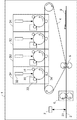
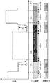
- 複数のパッチ画像を記録材に形成する画像形成手段と、
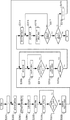
記録材に光を照射し、その反射光に含まれる各波長の光を光電変換して、各波長の光量を検出する分光データ検出手段と、
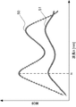
記録材に形成した前記複数のパッチ画像のうちの、互いに隣接する2つのパッチ画像の境界を、前記分光データ検出手段が検出する少なくとも1つの注目波長の光量の変化から判定する境界判定手段と、
パッチ画像の色値を、前記分光データ検出手段が該パッチ画像に光を照射して検出した各波長の光量から算出する色値算出手段と、
前記分光データ検出手段の光電変換における電荷の蓄積時間を制御する制御手段と、
を備えており、
前記制御手段は、前記互いに隣接する2つのパッチ画像の境界を判定する際の前記分光データ検出手段での蓄積時間を、該2つのパッチ画像の色値を算出する際の蓄積時間より短くすることを特徴とする画像形成装置。 - 前記境界判定手段は、前記分光データ検出手段が検出する各波長のうちすべての波長ではなく少なくとも1つの注目波長の光量の変化から境界を判定することを特徴とする請求項1に記載の画像形成装置。
- 前記境界判定手段が境界を判定する際の前記分光データ検出手段での蓄積時間は、前記分光データ検出手段が検出する前記少なくとも1つの注目波長の光量が所定の閾値より大きくなる様に決定されることを特徴とする請求項1又は2に記載の画像形成装置。
- 前記色値算出手段が色値を算出する際の前記分光データ検出手段での蓄積時間は、前記複数のパッチ画像のそれぞれに対して個別に設定されることを特徴とする請求項1から3のいずれか1項に記載の画像形成装置。
- 前記色値算出手段が色値を算出する際の前記分光データ検出手段での蓄積時間は、色値の算出対象であるパッチ画像の反射率が高くなるほど短くなることを特徴とする請求項4に記載の画像形成装置。
- 前記境界判定手段が境界を判定する際の前記分光データ検出手段での蓄積時間は、前記複数のパッチ画像のうちの、互いに隣接する2つのパッチ画像の境界それぞれに対して個別に設定されることを特徴とする請求項1から5のいずれか1項に記載の画像形成装置。
- 前記境界判定手段が境界を判定する際の前記分光データ検出手段での蓄積時間は、検出対象の境界の両側のパッチ画像の反射率が高くなるほど短くなることを特徴とする請求項6に記載の画像形成装置。
- 前記境界判定手段が、前記少なくとも1つの注目波長の光量を示すデータを前記分光データ検出手段から取得すると、前記制御手段は、前記分光データ検出手段に対して光量を示すデータの出力を停止させる制御を行うことを特徴とする請求項1から7のいずれか1項に記載の画像形成装置。
- 前記境界判定手段が境界を判定する際、前記制御手段は、前記分光データ検出手段が前記少なくとも1つの注目波長の光量のみを出力する様に前記分光データ検出手段を制御することを特徴とする請求項1から7のいずれか1項に記載の画像形成装置。
- 記録材としての紙の上に形成された画像を定着する定着手段をさらに備え、
前記パッチ画像は紙の上に形成され、前記定着手段により定着された後、前記画像形成装置から排出される前に前記分光データ検出手段により検出されることを特徴とする請求項1から9のいずれか1項に記載の画像形成装置。 - 色味を検出するための複数のパッチ画像を記録材に形成する画像形成手段と、
記録材に光を照射し、その反射光に含まれる各波長の光を光電変換して、各波長の光量を検出する分光データ検出手段と、
を備えており、
前記複数のパッチ画像の互いに隣接する2つのパッチ画像の境界を判定するための少なくとも1つの注目波長の光量を検出する際の、前記分光データ検出手段の光電変換における電荷の蓄積時間を、前記複数のパッチ画像の各パッチ画像の色値を算出するために各波長の光量を検出する際の、各パッチ画像に対応する前記分光データ検出手段の光電変換における電荷の蓄積時間より短くすることを特徴とする画像形成装置。 - 記録材としての紙の上に形成された画像を定着する定着手段をさらに備え、
前記パッチ画像は紙の上に形成され、前記定着手段により定着された後、前記画像形成装置から排出される前に前記分光データ検出手段により検出されることを特徴とする請求項11に記載の画像形成装置。
Priority Applications (2)
| Application Number | Priority Date | Filing Date | Title |
|---|---|---|---|
| JP2011139857A JP5804795B2 (ja) | 2011-06-23 | 2011-06-23 | 画像形成装置 |
| US13/492,600 US9031431B2 (en) | 2011-06-23 | 2012-06-08 | Image forming apparatus with spectral data detection unit |
Applications Claiming Priority (1)
| Application Number | Priority Date | Filing Date | Title |
|---|---|---|---|
| JP2011139857A JP5804795B2 (ja) | 2011-06-23 | 2011-06-23 | 画像形成装置 |
Publications (3)
| Publication Number | Publication Date |
|---|---|
| JP2013007859A JP2013007859A (ja) | 2013-01-10 |
| JP2013007859A5 JP2013007859A5 (ja) | 2014-07-31 |
| JP5804795B2 true JP5804795B2 (ja) | 2015-11-04 |
Family
ID=47361967
Family Applications (1)
| Application Number | Title | Priority Date | Filing Date |
|---|---|---|---|
| JP2011139857A Expired - Fee Related JP5804795B2 (ja) | 2011-06-23 | 2011-06-23 | 画像形成装置 |
Country Status (2)
| Country | Link |
|---|---|
| US (1) | US9031431B2 (ja) |
| JP (1) | JP5804795B2 (ja) |
Families Citing this family (6)
| Publication number | Priority date | Publication date | Assignee | Title |
|---|---|---|---|---|
| JP4965961B2 (ja) * | 2006-10-12 | 2012-07-04 | キヤノン株式会社 | 画像形成装置 |
| JP5796971B2 (ja) * | 2011-02-28 | 2015-10-21 | キヤノン株式会社 | 画像形成装置 |
| GB201221124D0 (en) * | 2012-11-23 | 2013-01-09 | Kromek Ltd | Method of spectral data detection and manipulation |
| JP5991775B2 (ja) * | 2013-02-20 | 2016-09-14 | キヤノン株式会社 | 測定装置、および画像形成装置 |
| JP6217695B2 (ja) * | 2015-06-09 | 2017-10-25 | コニカミノルタ株式会社 | 測色装置、画像形成装置、画像形成システムおよび画像形成管理装置 |
| JP7229782B2 (ja) * | 2019-01-09 | 2023-02-28 | キヤノン株式会社 | 測定装置及び画像形成システム |
Family Cites Families (11)
| Publication number | Priority date | Publication date | Assignee | Title |
|---|---|---|---|---|
| US7280207B2 (en) * | 2001-07-25 | 2007-10-09 | Applera Corporation | Time-delay integration in a flow cytometry system |
| EP1437631B1 (en) * | 2002-11-29 | 2008-09-10 | Ricoh Company, Ltd. | Method of determining the minimum usable acceptance width of alignment pattern detecting sensor for an image forming apparatus |
| JP2004245931A (ja) * | 2003-02-12 | 2004-09-02 | Canon Inc | カラー画像形成装置およびカラー画像形成装置の測色制御方法およびコンピュータが読み取り可能な記憶媒体およびプログラム |
| JP4280591B2 (ja) * | 2003-09-29 | 2009-06-17 | キヤノン株式会社 | 光学センサの制御方法及び制御装置 |
| JP4280725B2 (ja) * | 2005-04-27 | 2009-06-17 | キヤノン株式会社 | 画像形成装置及びその制御方法 |
| JP4898260B2 (ja) * | 2006-04-03 | 2012-03-14 | キヤノン株式会社 | 画像形成装置 |
| JP2009069233A (ja) * | 2007-09-11 | 2009-04-02 | Kyocera Mita Corp | カラー画像形成装置 |
| JP2010091600A (ja) * | 2008-10-03 | 2010-04-22 | Canon Inc | 画像形成装置 |
| JP5230458B2 (ja) * | 2009-01-20 | 2013-07-10 | 京セラドキュメントソリューションズ株式会社 | 画像形成装置 |
| JP5864866B2 (ja) * | 2011-02-10 | 2016-02-17 | キヤノン株式会社 | 画像形成装置 |
| JP5796971B2 (ja) * | 2011-02-28 | 2015-10-21 | キヤノン株式会社 | 画像形成装置 |
-
2011
- 2011-06-23 JP JP2011139857A patent/JP5804795B2/ja not_active Expired - Fee Related
-
2012
- 2012-06-08 US US13/492,600 patent/US9031431B2/en not_active Expired - Fee Related
Also Published As
| Publication number | Publication date |
|---|---|
| US20120328312A1 (en) | 2012-12-27 |
| US9031431B2 (en) | 2015-05-12 |
| JP2013007859A (ja) | 2013-01-10 |
Similar Documents
| Publication | Publication Date | Title |
|---|---|---|
| JP5804795B2 (ja) | 画像形成装置 | |
| US8797600B2 (en) | Image forming apparatus and gradation correction method with density unevenness detection | |
| JP5796971B2 (ja) | 画像形成装置 | |
| US20130148138A1 (en) | Image forming apparatus and gradation correction method for the same | |
| US9459579B2 (en) | Image forming apparatus that corrects image forming condition based on measurement result of measurement image | |
| JP4935657B2 (ja) | 画像形成装置 | |
| US9020377B2 (en) | Image forming with abnormity detection | |
| US10620577B2 (en) | Method for controlling density of image to be formed by image forming apparatus having developer and humidity sensors | |
| US9372460B2 (en) | Image forming apparatus holding tone correction table | |
| US20180173145A1 (en) | Image forming apparatus including sensor having substrate on which light-emitting element and light-receiving element are provided | |
| US10739700B2 (en) | Image forming apparatus | |
| JP5257235B2 (ja) | 画像形成装置及び色ずれ補正方法 | |
| US10241434B2 (en) | Image forming apparatus and position detection method | |
| JP2005300758A (ja) | 画像形成装置及びその制御方法 | |
| JP2013167718A (ja) | 制御装置、画像形成装置及びプログラム | |
| JP5157875B2 (ja) | 画像形成装置、色ずれ補正方法、プログラムおよび記録媒体 | |
| JP5998567B2 (ja) | 濃度検出装置及び画像形成装置 | |
| JP7325493B2 (ja) | 記録材判定装置及び画像形成装置 | |
| JP5187286B2 (ja) | 画像形成装置 | |
| US20190025743A1 (en) | Image forming apparatus and method of controlling image forming apparatus allowing correction of gradation level | |
| US11847363B2 (en) | Image forming apparatus that executes calibration | |
| US11619898B2 (en) | Image forming apparatus for controlling transfer voltage based on pattern | |
| JP2013140311A (ja) | 画像形成装置 | |
| JP6769056B2 (ja) | 画像形成システム及びプログラム | |
| JP2005091591A (ja) | 画像形成装置、及びその制御方法、プログラム及び記憶媒体 |
Legal Events
| Date | Code | Title | Description |
|---|---|---|---|
| A521 | Written amendment |
Free format text: JAPANESE INTERMEDIATE CODE: A523 Effective date: 20140613 |
|
| A621 | Written request for application examination |
Free format text: JAPANESE INTERMEDIATE CODE: A621 Effective date: 20140613 |
|
| A131 | Notification of reasons for refusal |
Free format text: JAPANESE INTERMEDIATE CODE: A131 Effective date: 20150327 |
|
| A521 | Written amendment |
Free format text: JAPANESE INTERMEDIATE CODE: A523 Effective date: 20150520 |
|
| TRDD | Decision of grant or rejection written | ||
| A01 | Written decision to grant a patent or to grant a registration (utility model) |
Free format text: JAPANESE INTERMEDIATE CODE: A01 Effective date: 20150803 |
|
| A61 | First payment of annual fees (during grant procedure) |
Free format text: JAPANESE INTERMEDIATE CODE: A61 Effective date: 20150901 |
|
| LAPS | Cancellation because of no payment of annual fees |