JP5752639B2 - 接合システム、接合方法、プログラム及びコンピュータ記憶媒体 - Google Patents
接合システム、接合方法、プログラム及びコンピュータ記憶媒体 Download PDFInfo
- Publication number
- JP5752639B2 JP5752639B2 JP2012121188A JP2012121188A JP5752639B2 JP 5752639 B2 JP5752639 B2 JP 5752639B2 JP 2012121188 A JP2012121188 A JP 2012121188A JP 2012121188 A JP2012121188 A JP 2012121188A JP 5752639 B2 JP5752639 B2 JP 5752639B2
- Authority
- JP
- Japan
- Prior art keywords
- substrate
- processed
- wafer
- adhesive
- heat treatment
- Prior art date
- Legal status (The legal status is an assumption and is not a legal conclusion. Google has not performed a legal analysis and makes no representation as to the accuracy of the status listed.)
- Active
Links
Images


Classifications
-
- H—ELECTRICITY
- H01—ELECTRIC ELEMENTS
- H01L—SEMICONDUCTOR DEVICES NOT COVERED BY CLASS H10
- H01L21/00—Processes or apparatus adapted for the manufacture or treatment of semiconductor or solid state devices or of parts thereof
- H01L21/67—Apparatus specially adapted for handling semiconductor or electric solid state devices during manufacture or treatment thereof; Apparatus specially adapted for handling wafers during manufacture or treatment of semiconductor or electric solid state devices or components ; Apparatus not specifically provided for elsewhere
- H01L21/67005—Apparatus not specifically provided for elsewhere
- H01L21/67011—Apparatus for manufacture or treatment
- H01L21/67121—Apparatus for making assemblies not otherwise provided for, e.g. package constructions
-
- H—ELECTRICITY
- H01—ELECTRIC ELEMENTS
- H01L—SEMICONDUCTOR DEVICES NOT COVERED BY CLASS H10
- H01L21/00—Processes or apparatus adapted for the manufacture or treatment of semiconductor or solid state devices or of parts thereof
- H01L21/67—Apparatus specially adapted for handling semiconductor or electric solid state devices during manufacture or treatment thereof; Apparatus specially adapted for handling wafers during manufacture or treatment of semiconductor or electric solid state devices or components ; Apparatus not specifically provided for elsewhere
- H01L21/683—Apparatus specially adapted for handling semiconductor or electric solid state devices during manufacture or treatment thereof; Apparatus specially adapted for handling wafers during manufacture or treatment of semiconductor or electric solid state devices or components ; Apparatus not specifically provided for elsewhere for supporting or gripping
-
- H—ELECTRICITY
- H01—ELECTRIC ELEMENTS
- H01L—SEMICONDUCTOR DEVICES NOT COVERED BY CLASS H10
- H01L21/00—Processes or apparatus adapted for the manufacture or treatment of semiconductor or solid state devices or of parts thereof
- H01L21/02—Manufacture or treatment of semiconductor devices or of parts thereof
- H01L21/04—Manufacture or treatment of semiconductor devices or of parts thereof the devices having at least one potential-jump barrier or surface barrier, e.g. PN junction, depletion layer or carrier concentration layer
- H01L21/18—Manufacture or treatment of semiconductor devices or of parts thereof the devices having at least one potential-jump barrier or surface barrier, e.g. PN junction, depletion layer or carrier concentration layer the devices having semiconductor bodies comprising elements of Group IV of the Periodic System or AIIIBV compounds with or without impurities, e.g. doping materials
- H01L21/185—Joining of semiconductor bodies for junction formation
-
- H—ELECTRICITY
- H01—ELECTRIC ELEMENTS
- H01L—SEMICONDUCTOR DEVICES NOT COVERED BY CLASS H10
- H01L21/00—Processes or apparatus adapted for the manufacture or treatment of semiconductor or solid state devices or of parts thereof
- H01L21/67—Apparatus specially adapted for handling semiconductor or electric solid state devices during manufacture or treatment thereof; Apparatus specially adapted for handling wafers during manufacture or treatment of semiconductor or electric solid state devices or components ; Apparatus not specifically provided for elsewhere
- H01L21/67005—Apparatus not specifically provided for elsewhere
- H01L21/67011—Apparatus for manufacture or treatment
- H01L21/67017—Apparatus for fluid treatment
- H01L21/67028—Apparatus for fluid treatment for cleaning followed by drying, rinsing, stripping, blasting or the like
- H01L21/6704—Apparatus for fluid treatment for cleaning followed by drying, rinsing, stripping, blasting or the like for wet cleaning or washing
- H01L21/67051—Apparatus for fluid treatment for cleaning followed by drying, rinsing, stripping, blasting or the like for wet cleaning or washing using mainly spraying means, e.g. nozzles
-
- H—ELECTRICITY
- H01—ELECTRIC ELEMENTS
- H01L—SEMICONDUCTOR DEVICES NOT COVERED BY CLASS H10
- H01L21/00—Processes or apparatus adapted for the manufacture or treatment of semiconductor or solid state devices or of parts thereof
- H01L21/67—Apparatus specially adapted for handling semiconductor or electric solid state devices during manufacture or treatment thereof; Apparatus specially adapted for handling wafers during manufacture or treatment of semiconductor or electric solid state devices or components ; Apparatus not specifically provided for elsewhere
- H01L21/67005—Apparatus not specifically provided for elsewhere
- H01L21/67011—Apparatus for manufacture or treatment
- H01L21/67092—Apparatus for mechanical treatment
-
- H—ELECTRICITY
- H01—ELECTRIC ELEMENTS
- H01L—SEMICONDUCTOR DEVICES NOT COVERED BY CLASS H10
- H01L21/00—Processes or apparatus adapted for the manufacture or treatment of semiconductor or solid state devices or of parts thereof
- H01L21/67—Apparatus specially adapted for handling semiconductor or electric solid state devices during manufacture or treatment thereof; Apparatus specially adapted for handling wafers during manufacture or treatment of semiconductor or electric solid state devices or components ; Apparatus not specifically provided for elsewhere
- H01L21/67005—Apparatus not specifically provided for elsewhere
- H01L21/67011—Apparatus for manufacture or treatment
- H01L21/67098—Apparatus for thermal treatment
- H01L21/67109—Apparatus for thermal treatment mainly by convection
-
- H—ELECTRICITY
- H01—ELECTRIC ELEMENTS
- H01L—SEMICONDUCTOR DEVICES NOT COVERED BY CLASS H10
- H01L21/00—Processes or apparatus adapted for the manufacture or treatment of semiconductor or solid state devices or of parts thereof
- H01L21/67—Apparatus specially adapted for handling semiconductor or electric solid state devices during manufacture or treatment thereof; Apparatus specially adapted for handling wafers during manufacture or treatment of semiconductor or electric solid state devices or components ; Apparatus not specifically provided for elsewhere
- H01L21/67005—Apparatus not specifically provided for elsewhere
- H01L21/67011—Apparatus for manufacture or treatment
- H01L21/6715—Apparatus for applying a liquid, a resin, an ink or the like
-
- H—ELECTRICITY
- H01—ELECTRIC ELEMENTS
- H01L—SEMICONDUCTOR DEVICES NOT COVERED BY CLASS H10
- H01L21/00—Processes or apparatus adapted for the manufacture or treatment of semiconductor or solid state devices or of parts thereof
- H01L21/67—Apparatus specially adapted for handling semiconductor or electric solid state devices during manufacture or treatment thereof; Apparatus specially adapted for handling wafers during manufacture or treatment of semiconductor or electric solid state devices or components ; Apparatus not specifically provided for elsewhere
- H01L21/67005—Apparatus not specifically provided for elsewhere
- H01L21/67011—Apparatus for manufacture or treatment
- H01L21/67155—Apparatus for manufacturing or treating in a plurality of work-stations
- H01L21/67161—Apparatus for manufacturing or treating in a plurality of work-stations characterized by the layout of the process chambers
- H01L21/67178—Apparatus for manufacturing or treating in a plurality of work-stations characterized by the layout of the process chambers vertical arrangement
-
- H—ELECTRICITY
- H01—ELECTRIC ELEMENTS
- H01L—SEMICONDUCTOR DEVICES NOT COVERED BY CLASS H10
- H01L21/00—Processes or apparatus adapted for the manufacture or treatment of semiconductor or solid state devices or of parts thereof
- H01L21/67—Apparatus specially adapted for handling semiconductor or electric solid state devices during manufacture or treatment thereof; Apparatus specially adapted for handling wafers during manufacture or treatment of semiconductor or electric solid state devices or components ; Apparatus not specifically provided for elsewhere
- H01L21/677—Apparatus specially adapted for handling semiconductor or electric solid state devices during manufacture or treatment thereof; Apparatus specially adapted for handling wafers during manufacture or treatment of semiconductor or electric solid state devices or components ; Apparatus not specifically provided for elsewhere for conveying, e.g. between different workstations
- H01L21/67739—Apparatus specially adapted for handling semiconductor or electric solid state devices during manufacture or treatment thereof; Apparatus specially adapted for handling wafers during manufacture or treatment of semiconductor or electric solid state devices or components ; Apparatus not specifically provided for elsewhere for conveying, e.g. between different workstations into and out of processing chamber
- H01L21/67742—Mechanical parts of transfer devices
-
- H—ELECTRICITY
- H01—ELECTRIC ELEMENTS
- H01L—SEMICONDUCTOR DEVICES NOT COVERED BY CLASS H10
- H01L21/00—Processes or apparatus adapted for the manufacture or treatment of semiconductor or solid state devices or of parts thereof
- H01L21/67—Apparatus specially adapted for handling semiconductor or electric solid state devices during manufacture or treatment thereof; Apparatus specially adapted for handling wafers during manufacture or treatment of semiconductor or electric solid state devices or components ; Apparatus not specifically provided for elsewhere
- H01L21/683—Apparatus specially adapted for handling semiconductor or electric solid state devices during manufacture or treatment thereof; Apparatus specially adapted for handling wafers during manufacture or treatment of semiconductor or electric solid state devices or components ; Apparatus not specifically provided for elsewhere for supporting or gripping
- H01L21/6835—Apparatus specially adapted for handling semiconductor or electric solid state devices during manufacture or treatment thereof; Apparatus specially adapted for handling wafers during manufacture or treatment of semiconductor or electric solid state devices or components ; Apparatus not specifically provided for elsewhere for supporting or gripping using temporarily an auxiliary support
-
- H—ELECTRICITY
- H01—ELECTRIC ELEMENTS
- H01L—SEMICONDUCTOR DEVICES NOT COVERED BY CLASS H10
- H01L2221/00—Processes or apparatus adapted for the manufacture or treatment of semiconductor or solid state devices or of parts thereof covered by H01L21/00
- H01L2221/67—Apparatus for handling semiconductor or electric solid state devices during manufacture or treatment thereof; Apparatus for handling wafers during manufacture or treatment of semiconductor or electric solid state devices or components; Apparatus not specifically provided for elsewhere
- H01L2221/683—Apparatus for handling semiconductor or electric solid state devices during manufacture or treatment thereof; Apparatus for handling wafers during manufacture or treatment of semiconductor or electric solid state devices or components; Apparatus not specifically provided for elsewhere for supporting or gripping
- H01L2221/68304—Apparatus for handling semiconductor or electric solid state devices during manufacture or treatment thereof; Apparatus for handling wafers during manufacture or treatment of semiconductor or electric solid state devices or components; Apparatus not specifically provided for elsewhere for supporting or gripping using temporarily an auxiliary support
- H01L2221/68318—Auxiliary support including means facilitating the separation of a device or wafer from the auxiliary support
-
- H—ELECTRICITY
- H01—ELECTRIC ELEMENTS
- H01L—SEMICONDUCTOR DEVICES NOT COVERED BY CLASS H10
- H01L2221/00—Processes or apparatus adapted for the manufacture or treatment of semiconductor or solid state devices or of parts thereof covered by H01L21/00
- H01L2221/67—Apparatus for handling semiconductor or electric solid state devices during manufacture or treatment thereof; Apparatus for handling wafers during manufacture or treatment of semiconductor or electric solid state devices or components; Apparatus not specifically provided for elsewhere
- H01L2221/683—Apparatus for handling semiconductor or electric solid state devices during manufacture or treatment thereof; Apparatus for handling wafers during manufacture or treatment of semiconductor or electric solid state devices or components; Apparatus not specifically provided for elsewhere for supporting or gripping
- H01L2221/68304—Apparatus for handling semiconductor or electric solid state devices during manufacture or treatment thereof; Apparatus for handling wafers during manufacture or treatment of semiconductor or electric solid state devices or components; Apparatus not specifically provided for elsewhere for supporting or gripping using temporarily an auxiliary support
- H01L2221/68327—Apparatus for handling semiconductor or electric solid state devices during manufacture or treatment thereof; Apparatus for handling wafers during manufacture or treatment of semiconductor or electric solid state devices or components; Apparatus not specifically provided for elsewhere for supporting or gripping using temporarily an auxiliary support used during dicing or grinding
-
- H—ELECTRICITY
- H01—ELECTRIC ELEMENTS
- H01L—SEMICONDUCTOR DEVICES NOT COVERED BY CLASS H10
- H01L2221/00—Processes or apparatus adapted for the manufacture or treatment of semiconductor or solid state devices or of parts thereof covered by H01L21/00
- H01L2221/67—Apparatus for handling semiconductor or electric solid state devices during manufacture or treatment thereof; Apparatus for handling wafers during manufacture or treatment of semiconductor or electric solid state devices or components; Apparatus not specifically provided for elsewhere
- H01L2221/683—Apparatus for handling semiconductor or electric solid state devices during manufacture or treatment thereof; Apparatus for handling wafers during manufacture or treatment of semiconductor or electric solid state devices or components; Apparatus not specifically provided for elsewhere for supporting or gripping
- H01L2221/68304—Apparatus for handling semiconductor or electric solid state devices during manufacture or treatment thereof; Apparatus for handling wafers during manufacture or treatment of semiconductor or electric solid state devices or components; Apparatus not specifically provided for elsewhere for supporting or gripping using temporarily an auxiliary support
- H01L2221/6834—Apparatus for handling semiconductor or electric solid state devices during manufacture or treatment thereof; Apparatus for handling wafers during manufacture or treatment of semiconductor or electric solid state devices or components; Apparatus not specifically provided for elsewhere for supporting or gripping using temporarily an auxiliary support used to protect an active side of a device or wafer
Description
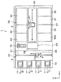
2 搬入出ステーション
3 処理ステーション
30〜33 接合装置
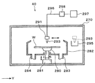
40 接着剤塗布装置
41 保護剤塗布装置
42 剥離剤塗布装置
43 熱処理装置
60 ウェハ搬送領域
293 接着剤ノズル
360 制御部
400 塗布装置
434 接着剤ノズル
438 保護剤ノズル
441 剥離剤ノズル
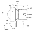
500 熱処理装置
511 ガス供給口
530 加熱機構
540 温度調節機構
550 熱処理板
551 外周領域
552 中心領域
G 接着剤
P 保護剤
R 剥離剤
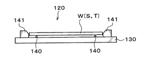
S 支持ウェハ
T 重合ウェハ
W 被処理ウェハ
Claims (23)
- 被処理基板と支持基板を接合する接合システムであって、
被処理基板と支持基板に所定の処理を行う処理ステーションと、
被処理基板、支持基板、又は被処理基板と支持基板が接合された重合基板を、前記処理ステーションに対して搬入出する搬入出ステーションと、を有し、
前記処理ステーションは、
被処理基板又は支持基板に接着剤を塗布する接着剤供給部と、
被処理基板と支持基板の間において前記接着剤よりも被処理基板側に塗布されるように、当該被処理基板に保護剤を塗布する保護剤供給部と、
被処理基板と支持基板の間において前記接着剤よりも支持基板側に塗布されるように、当該被処理基板又は支持基板に剥離剤を塗布する剥離剤供給部と、
少なくとも前記接着剤、前記保護剤又は前記剥離剤が塗布された、被処理基板又は支持基板を所定の温度に加熱する熱処理装置と、
前記接着剤、前記保護剤及び前記剥離剤を介して、被処理基板と支持基板を接合する接合装置と、
前記接着剤供給部、前記保護剤供給部、前記剥離剤供給部、前記熱処理装置及び前記接合装置に対して、被処理基板、支持基板又は重合基板を搬送するための搬送領域と、を有することを特徴とする、接合システム。 - 前記処理ステーションは、前記接着剤供給部を備えた接着剤塗布装置と、前記保護剤供給部を備えた保護剤塗布装置と、前記剥離剤供給部を備えた剥離剤塗布装置とを有することを特徴とする、請求項1に記載の接合システム。
- 前記接着剤塗布装置、前記保護剤塗布装置及び前記剥離剤塗布装置は、前記接着剤、前記保護剤及び前記剥離剤の粘度の高い順に鉛直方向に下方から積層されて配置されていることを特徴とする、請求項2に記載の接合システム。
- 前記接着剤塗布装置、前記保護剤塗布装置及び前記剥離剤塗布装置は、平面視において並べて配置されていることを特徴とする、請求項2に記載の接合システム。
- 前記処理ステーションは、前記接着剤供給部、前記保護剤供給部及び前記剥離剤供給部を備えた塗布装置を有することを特徴とする、請求項1に記載の接合システム。
- 被処理基板と支持基板を接合する接合システムであって、
被処理基板と支持基板に所定の処理を行う処理ステーションと、
被処理基板、支持基板、又は被処理基板と支持基板が接合された重合基板を、前記処理ステーションに対して搬入出する搬入出ステーションと、を有し、
前記処理ステーションは、
被処理基板又は支持基板に接着剤を塗布する接着剤供給部を備えた接着剤塗布装置と、
被処理基板と支持基板の間において前記接着剤よりも支持基板側に塗布されるように、当該被処理基板又は支持基板に剥離剤を塗布する剥離剤供給部を備えた剥離剤塗布装置と、
少なくとも前記接着剤又は前記剥離剤が塗布された、被処理基板又は支持基板を所定の温度に加熱する熱処理装置と、
前記接着剤と前記剥離剤を介して、被処理基板と支持基板を接合する接合装置と、
前記接着剤供給部、前記剥離剤供給部、前記熱処理装置及び前記接合装置に対して、被処理基板、支持基板又は重合基板を搬送するための搬送領域と、を有し、
前記接着剤塗布装置と前記剥離剤塗布装置は、鉛直方向に下方からこの順で積層されて配置されていることを特徴とする、接合システム。 - 前記処理ステーションは、前記接合装置で接合された重合基板に対して、当該重合基板の外周部を中心部よりも高い温度で熱処理を行う他の熱処理装置を有することを特徴とする、請求項1〜6のいずれかに記載の接合システム。
- 前記他の熱処理装置は、前記重合基板の外周部を加熱する環状の加熱機構を有することを特徴とする、請求項7に記載の接合システム。
- 前記他の熱処理装置は、前記加熱機構の内側に設けられ、前記重合基板の中心部を所定の温度に調節する温度調節機構を有することを特徴とする、請求項8に記載の接合システム。
- 前記他の熱処理装置は、重合基板を載置して加熱する熱処理板を有し、
前記熱処理板は、前記重合基板の外周部を加熱する外周領域と、前記外周領域の内側に設けられ、前記重合基板の中心部を加熱する中心領域とに区画され、
前記外周領域の加熱温度は、前記中心領域の加熱温度よりも高いことを特徴とする、請求項7に記載の接合システム。 - 前記他の熱処理装置は、複数の重合基板を収容して熱処理可能であることを特徴とする、請求項7〜10のいずれかに記載の接合システム。
- 前記他の熱処理装置の内部は、不活性ガス雰囲気に維持可能であることを特徴とする、請求項7〜11のいずれかに記載の接合システム。
- 接合システムを用いて被処理基板と支持基板を接合する接合方法であって、
前記接合システムは、
被処理基板又は支持基板に接着剤を塗布する接着剤供給部と、被処理基板と支持基板の間において前記接着剤よりも被処理基板側に塗布されるように、当該被処理基板に保護剤を塗布する保護剤供給部と、被処理基板と支持基板の間において前記接着剤よりも支持基板側に塗布されるように、当該被処理基板又は支持基板に剥離剤を塗布する剥離剤供給部と、少なくとも前記接着剤、前記保護剤又は前記剥離剤が塗布された、被処理基板又は支持基板を所定の温度に加熱する熱処理装置と、前記接着剤、前記保護剤及び前記剥離剤を介して、被処理基板と支持基板を接合する接合装置と、前記接着剤供給部、前記保護剤供給部、前記剥離剤供給部、前記熱処理装置及び前記接合装置に対して、被処理基板、支持基板又は被処理基板と支持基板が接合された重合基板を搬送するための搬送領域と、を備えた処理ステーションと、
被処理基板、支持基板又は重合基板を、前記処理ステーションに対して搬入出する搬入出ステーションと、を有し、
前記接合方法は、
前記保護剤供給部で被処理基板に前記保護剤を塗布した後、前記熱処理装置で当該被処理基板を所定の温度に加熱する保護剤塗布工程と、
前記接着剤供給部で被処理基板又は支持基板に前記接着剤を塗布した後、前記熱処理装置で当該被処理基板又は支持基板を所定の温度に加熱する接着剤塗布工程と、
前記剥離剤供給部で被処理基板又は支持基板に前記剥離剤を塗布した後、前記熱処理装置で当該被処理基板又は支持基板を所定の温度に加熱する剥離剤塗布工程と、
その後、前記接合装置において、前記接着剤、前記保護剤及び前記剥離剤を介して、被処理基板と支持基板を接合する接合工程と、を有することを特徴とする、接合方法。 - 前記処理ステーションは、前記接着剤供給部を備えた接着剤塗布装置と、前記保護剤供給部を備えた保護剤塗布装置と、前記剥離剤供給部を備えた剥離剤塗布装置とを有し、
前記接着剤塗布工程において、前記接着剤塗布装置で被処理基板又は支持基板に前記接着剤を塗布した後、前記熱処理装置で当該被処理基板又は支持基板を所定の温度に加熱し、
前記保護剤塗布工程において、前記保護剤塗布装置で被処理基板に前記保護剤を塗布した後、前記熱処理装置で当該被処理基板を所定の温度に加熱し、
前記剥離剤塗布工程において、前記剥離剤塗布装置で被処理基板又は支持基板に前記剥離剤を塗布した後、前記熱処理装置で当該被処理基板又は支持基板を所定の温度に加熱することを特徴とする、請求項13に記載の接合方法。 - 前記処理ステーションは、前記接着剤供給部、前記保護剤供給部及び前記剥離剤供給部を備えた塗布装置を有し、
前記接着剤塗布工程において、前記塗布装置で被処理基板又は支持基板に前記接着剤を塗布した後、前記熱処理装置で当該被処理基板又は支持基板を所定の温度に加熱し、
前記保護剤塗布工程において、前記塗布装置で被処理基板に前記保護剤を塗布した後、前記熱処理装置で当該被処理基板を所定の温度に加熱し、
前記剥離剤塗布工程において、前記塗布装置で被処理基板又は支持基板に前記剥離剤を塗布した後、前記熱処理装置で当該被処理基板又は支持基板を所定の温度に加熱することを特徴とする、請求項13に記載の接合方法。 - 前記接合工程後に、前記処理ステーションに設けられた他の熱処理装置において、前記接合工程で接合された重合基板に対して、当該重合基板の外周部を中心部よりも高い温度で熱処理を行う熱処理工程を有することを特徴とする、請求項13〜15のいずれかに記載の接合方法。
- 前記他の熱処理装置は、前記重合基板の外周部を加熱する環状の加熱機構を有し、
前記熱処理工程において、前記加熱機構によって前記重合基板の外周部を加熱することを特徴とする、請求項16に記載の接合方法。 - 前記他の熱処理装置は、前記加熱機構の内側に設けられ、前記重合基板の中心部を所定の温度に調節する温度調節機構を有し、
前記熱処理工程において、前記加熱機構によって前記重合基板の外周部を加熱すると共に、前記温度調節機構によって前記重合基板の中心部を所定の温度に調節することを特徴とする、請求項17に記載の接合方法。 - 前記他の熱処理装置は、重合基板を載置して加熱する熱処理板を有し、
前記熱処理板は、前記重合基板の外周部を加熱する外周領域と、前記外周領域の内側に設けられ、前記重合基板の中心部を加熱する中心領域とに区画され、
前記熱処理工程において、前記外周領域の加熱温度は前記中心領域の加熱温度よりも高いことを特徴とする、請求項16に記載の接合方法。 - 前記熱処理工程において、複数の重合基板を収容して熱処理することを特徴とする、請求項16〜19のいずれかに記載の接合方法。
- 前記熱処理工程において、前記他の熱処理装置の内部は、不活性ガス雰囲気に維持されていることを特徴とする、請求項16〜20のいずれかに記載の接合方法。
- 請求項13〜21のいずれかに記載の接合方法を接合システムによって実行させるように、当該接合システムを制御する制御部のコンピュータ上で動作するプログラム。
- 請求項22に記載のプログラムを格納した読み取り可能なコンピュータ記憶媒体。
Priority Applications (3)
| Application Number | Priority Date | Filing Date | Title |
|---|---|---|---|
| JP2012121188A JP5752639B2 (ja) | 2012-05-28 | 2012-05-28 | 接合システム、接合方法、プログラム及びコンピュータ記憶媒体 |
| US13/893,630 US8846495B2 (en) | 2012-05-28 | 2013-05-14 | Bonding system and bonding method |
| KR1020130055785A KR20130133129A (ko) | 2012-05-28 | 2013-05-16 | 접합 시스템, 접합 방법 및 컴퓨터 기억 매체 |
Applications Claiming Priority (1)
| Application Number | Priority Date | Filing Date | Title |
|---|---|---|---|
| JP2012121188A JP5752639B2 (ja) | 2012-05-28 | 2012-05-28 | 接合システム、接合方法、プログラム及びコンピュータ記憶媒体 |
Publications (3)
| Publication Number | Publication Date |
|---|---|
| JP2013247292A JP2013247292A (ja) | 2013-12-09 |
| JP2013247292A5 JP2013247292A5 (ja) | 2014-06-26 |
| JP5752639B2 true JP5752639B2 (ja) | 2015-07-22 |
Family
ID=49621920
Family Applications (1)
| Application Number | Title | Priority Date | Filing Date |
|---|---|---|---|
| JP2012121188A Active JP5752639B2 (ja) | 2012-05-28 | 2012-05-28 | 接合システム、接合方法、プログラム及びコンピュータ記憶媒体 |
Country Status (3)
| Country | Link |
|---|---|
| US (1) | US8846495B2 (ja) |
| JP (1) | JP5752639B2 (ja) |
| KR (1) | KR20130133129A (ja) |
Families Citing this family (18)
| Publication number | Priority date | Publication date | Assignee | Title |
|---|---|---|---|---|
| EP3011589B9 (de) * | 2013-06-17 | 2018-09-05 | Ev Group E. Thallner GmbH | Vorrichtung und verfahren zum ausrichten von substraten |
| JP5538613B1 (ja) * | 2013-11-13 | 2014-07-02 | 東京エレクトロン株式会社 | 接合装置及び接合システム |
| JP6145061B2 (ja) | 2014-03-04 | 2017-06-07 | 東京エレクトロン株式会社 | 接合システムおよび接合方法 |
| JP6228508B2 (ja) | 2014-05-01 | 2017-11-08 | 東京エレクトロン株式会社 | 洗浄装置、剥離システム、洗浄方法、プログラム及びコンピュータ記憶媒体 |
| JP6153886B2 (ja) * | 2014-05-09 | 2017-06-28 | 東京エレクトロン株式会社 | 洗浄装置、剥離システム、洗浄方法、プログラム及びコンピュータ記憶媒体 |
| JP6254054B2 (ja) * | 2014-08-21 | 2017-12-27 | 東京エレクトロン株式会社 | 塗布装置、接合システム、塗布方法、接合方法、プログラム、および情報記憶媒体 |
| DE102015108901A1 (de) * | 2015-06-05 | 2016-12-08 | Ev Group E. Thallner Gmbh | Verfahren zum Ausrichten von Substraten vor dem Bonden |
| JP6512986B2 (ja) | 2015-08-03 | 2019-05-15 | 東京エレクトロン株式会社 | 接合装置及び接合システム |
| JP2017034108A (ja) * | 2015-08-03 | 2017-02-09 | 東京エレクトロン株式会社 | 基板保持部材 |
| US10418264B2 (en) * | 2016-06-08 | 2019-09-17 | Hermes-Epitek Corporation | Assembling device used for semiconductor equipment |
| US20180068843A1 (en) * | 2016-09-07 | 2018-03-08 | Raytheon Company | Wafer stacking to form a multi-wafer-bonded structure |
| US10903066B2 (en) | 2017-05-08 | 2021-01-26 | Applied Materials, Inc. | Heater support kit for bevel etch chamber |
| US10300649B2 (en) | 2017-08-29 | 2019-05-28 | Raytheon Company | Enhancing die flatness |
| CN110838462B (zh) * | 2018-08-15 | 2022-12-13 | 北科天绘(合肥)激光技术有限公司 | 一种器件阵列的巨量转移方法及系统 |
| US10847569B2 (en) | 2019-02-26 | 2020-11-24 | Raytheon Company | Wafer level shim processing |
| US20230207331A1 (en) * | 2020-04-13 | 2023-06-29 | Tokyo Electron Limited | Bonding system |
| JP7008110B2 (ja) * | 2020-08-04 | 2022-01-25 | エーファウ・グループ・エー・タルナー・ゲーエムベーハー | 基板をボンディングするための方法および装置 |
| CN112403838A (zh) * | 2020-11-19 | 2021-02-26 | 合肥高地创意科技有限公司 | 一种集成电路保护带表面抗静电液涂覆装置 |
Family Cites Families (10)
| Publication number | Priority date | Publication date | Assignee | Title |
|---|---|---|---|---|
| JP3464005B2 (ja) * | 1991-08-16 | 2003-11-05 | 東京エレクトロン株式会社 | 熱処理方法 |
| JP3218164B2 (ja) * | 1995-05-31 | 2001-10-15 | 東京エレクトロン株式会社 | 被処理体の支持ボート、熱処理装置及び熱処理方法 |
| DE10320375B3 (de) * | 2003-05-07 | 2004-12-16 | Süss Micro Tec Laboratory Equipment GmbH | Verfahren zum temporären Fixieren zweier flächiger Werksücke |
| US7226812B2 (en) * | 2004-03-31 | 2007-06-05 | Intel Corporation | Wafer support and release in wafer processing |
| JP5027460B2 (ja) * | 2006-07-28 | 2012-09-19 | 東京応化工業株式会社 | ウエハの接着方法、薄板化方法、及び剥離方法 |
| JP2008182016A (ja) | 2007-01-24 | 2008-08-07 | Tokyo Electron Ltd | 貼り合わせ装置、貼り合わせ方法 |
| EP2238618B1 (en) * | 2008-01-24 | 2015-07-29 | Brewer Science, Inc. | Method for reversibly mounting a device wafer to a carrier substrate |
| JP2011040419A (ja) * | 2008-05-22 | 2011-02-24 | Fuji Electric Systems Co Ltd | 半導体装置の製造方法及びそのための装置 |
| US8764026B2 (en) * | 2009-04-16 | 2014-07-01 | Suss Microtec Lithography, Gmbh | Device for centering wafers |
| JP5379171B2 (ja) * | 2010-08-23 | 2013-12-25 | 東京エレクトロン株式会社 | 接合システム、基板処理システム、接合方法、プログラム及びコンピュータ記憶媒体 |
-
2012
- 2012-05-28 JP JP2012121188A patent/JP5752639B2/ja active Active
-
2013
- 2013-05-14 US US13/893,630 patent/US8846495B2/en not_active Expired - Fee Related
- 2013-05-16 KR KR1020130055785A patent/KR20130133129A/ko active IP Right Grant
Also Published As
| Publication number | Publication date |
|---|---|
| KR20130133129A (ko) | 2013-12-06 |
| JP2013247292A (ja) | 2013-12-09 |
| US8846495B2 (en) | 2014-09-30 |
| US20130316516A1 (en) | 2013-11-28 |
Similar Documents
| Publication | Publication Date | Title |
|---|---|---|
| JP5752639B2 (ja) | 接合システム、接合方法、プログラム及びコンピュータ記憶媒体 | |
| JP5485958B2 (ja) | 接合方法、プログラム、コンピュータ記憶媒体、接合装置及び接合システム | |
| JP5421967B2 (ja) | 接合方法、プログラム、コンピュータ記憶媒体及び接合システム | |
| JP5379171B2 (ja) | 接合システム、基板処理システム、接合方法、プログラム及びコンピュータ記憶媒体 | |
| JP5593299B2 (ja) | 接合装置、接合システム、接合方法、プログラム及びコンピュータ記憶媒体 | |
| JP5547147B2 (ja) | 接合装置、接合システム、接合方法、プログラム及びコンピュータ記憶媒体 | |
| JP5478565B2 (ja) | 接合システム | |
| JP5538282B2 (ja) | 接合装置、接合方法、プログラム及びコンピュータ記憶媒体 | |
| JP5406257B2 (ja) | 接合方法、プログラム、コンピュータ記憶媒体及び接合システム | |
| JP2013062431A (ja) | 接合装置、接合方法、接合システム、プログラム及びコンピュータ記憶媒体 | |
| JP5528405B2 (ja) | 接合方法、プログラム、コンピュータ記憶媒体及び接合システム | |
| JP5905509B2 (ja) | 接合装置、接合システム、接合方法、プログラム及びコンピュータ記憶媒体 | |
| JP5427856B2 (ja) | 接合方法、プログラム、コンピュータ記憶媒体及び接合システム | |
| JP5869960B2 (ja) | 接合システム、接合方法、プログラム及びコンピュータ記憶媒体 | |
| JP5552466B2 (ja) | 接合方法、プログラム、コンピュータ記憶媒体及び接合システム | |
| JP5905407B2 (ja) | シート剥離装置、接合システム、剥離システム、シート剥離方法、プログラム及びコンピュータ記憶媒体 | |
| JP2014056910A (ja) | 塗布処理装置、接合システム、塗布処理方法、プログラム及びコンピュータ記憶媒体 |
Legal Events
| Date | Code | Title | Description |
|---|---|---|---|
| A521 | Request for written amendment filed |
Free format text: JAPANESE INTERMEDIATE CODE: A523 Effective date: 20140513 |
|
| A621 | Written request for application examination |
Free format text: JAPANESE INTERMEDIATE CODE: A621 Effective date: 20140513 |
|
| A977 | Report on retrieval |
Free format text: JAPANESE INTERMEDIATE CODE: A971007 Effective date: 20140925 |
|
| A131 | Notification of reasons for refusal |
Free format text: JAPANESE INTERMEDIATE CODE: A131 Effective date: 20140930 |
|
| A521 | Request for written amendment filed |
Free format text: JAPANESE INTERMEDIATE CODE: A523 Effective date: 20141125 |
|
| TRDD | Decision of grant or rejection written | ||
| A01 | Written decision to grant a patent or to grant a registration (utility model) |
Free format text: JAPANESE INTERMEDIATE CODE: A01 Effective date: 20150512 |
|
| A61 | First payment of annual fees (during grant procedure) |
Free format text: JAPANESE INTERMEDIATE CODE: A61 Effective date: 20150520 |
|
| R150 | Certificate of patent or registration of utility model |
Ref document number: 5752639 Country of ref document: JP Free format text: JAPANESE INTERMEDIATE CODE: R150 |
|
| R250 | Receipt of annual fees |
Free format text: JAPANESE INTERMEDIATE CODE: R250 |
|
| R250 | Receipt of annual fees |
Free format text: JAPANESE INTERMEDIATE CODE: R250 |
|
| R250 | Receipt of annual fees |
Free format text: JAPANESE INTERMEDIATE CODE: R250 |
|
| R250 | Receipt of annual fees |
Free format text: JAPANESE INTERMEDIATE CODE: R250 |