JP5710088B2 - 半導体装置 - Google Patents
半導体装置 Download PDFInfo
- Publication number
- JP5710088B2 JP5710088B2 JP2006273325A JP2006273325A JP5710088B2 JP 5710088 B2 JP5710088 B2 JP 5710088B2 JP 2006273325 A JP2006273325 A JP 2006273325A JP 2006273325 A JP2006273325 A JP 2006273325A JP 5710088 B2 JP5710088 B2 JP 5710088B2
- Authority
- JP
- Japan
- Prior art keywords
- side wall
- light emitting
- wall
- emitting element
- lead electrode
- Prior art date
- Legal status (The legal status is an assumption and is not a legal conclusion. Google has not performed a legal analysis and makes no representation as to the accuracy of the status listed.)
- Expired - Fee Related
Links
Images

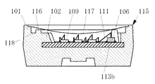


Classifications
-
- H—ELECTRICITY
- H10—SEMICONDUCTOR DEVICES; ELECTRIC SOLID-STATE DEVICES NOT OTHERWISE PROVIDED FOR
- H10W—GENERIC PACKAGES, INTERCONNECTIONS, CONNECTORS OR OTHER CONSTRUCTIONAL DETAILS OF DEVICES COVERED BY CLASS H10
- H10W72/00—Interconnections or connectors in packages
- H10W72/50—Bond wires
- H10W72/531—Shapes of wire connectors
- H10W72/536—Shapes of wire connectors the connected ends being ball-shaped
-
- H—ELECTRICITY
- H10—SEMICONDUCTOR DEVICES; ELECTRIC SOLID-STATE DEVICES NOT OTHERWISE PROVIDED FOR
- H10W—GENERIC PACKAGES, INTERCONNECTIONS, CONNECTORS OR OTHER CONSTRUCTIONAL DETAILS OF DEVICES COVERED BY CLASS H10
- H10W72/00—Interconnections or connectors in packages
- H10W72/50—Bond wires
- H10W72/531—Shapes of wire connectors
- H10W72/5363—Shapes of wire connectors the connected ends being wedge-shaped
-
- H—ELECTRICITY
- H10—SEMICONDUCTOR DEVICES; ELECTRIC SOLID-STATE DEVICES NOT OTHERWISE PROVIDED FOR
- H10W—GENERIC PACKAGES, INTERCONNECTIONS, CONNECTORS OR OTHER CONSTRUCTIONAL DETAILS OF DEVICES COVERED BY CLASS H10
- H10W72/00—Interconnections or connectors in packages
- H10W72/50—Bond wires
- H10W72/531—Shapes of wire connectors
- H10W72/5366—Shapes of wire connectors the bond wires having kinks
-
- H—ELECTRICITY
- H10—SEMICONDUCTOR DEVICES; ELECTRIC SOLID-STATE DEVICES NOT OTHERWISE PROVIDED FOR
- H10W—GENERIC PACKAGES, INTERCONNECTIONS, CONNECTORS OR OTHER CONSTRUCTIONAL DETAILS OF DEVICES COVERED BY CLASS H10
- H10W90/00—Package configurations
- H10W90/701—Package configurations characterised by the relative positions of pads or connectors relative to package parts
- H10W90/751—Package configurations characterised by the relative positions of pads or connectors relative to package parts of bond wires
- H10W90/756—Package configurations characterised by the relative positions of pads or connectors relative to package parts of bond wires between a chip and a stacked lead frame, conducting package substrate or heat sink
Landscapes
- Led Device Packages (AREA)
- Led Devices (AREA)
Priority Applications (1)
| Application Number | Priority Date | Filing Date | Title |
|---|---|---|---|
| JP2006273325A JP5710088B2 (ja) | 2006-10-04 | 2006-10-04 | 半導体装置 |
Applications Claiming Priority (1)
| Application Number | Priority Date | Filing Date | Title |
|---|---|---|---|
| JP2006273325A JP5710088B2 (ja) | 2006-10-04 | 2006-10-04 | 半導体装置 |
Publications (3)
| Publication Number | Publication Date |
|---|---|
| JP2008091792A JP2008091792A (ja) | 2008-04-17 |
| JP2008091792A5 JP2008091792A5 (enExample) | 2009-11-19 |
| JP5710088B2 true JP5710088B2 (ja) | 2015-04-30 |
Family
ID=39375606
Family Applications (1)
| Application Number | Title | Priority Date | Filing Date |
|---|---|---|---|
| JP2006273325A Expired - Fee Related JP5710088B2 (ja) | 2006-10-04 | 2006-10-04 | 半導体装置 |
Country Status (1)
| Country | Link |
|---|---|
| JP (1) | JP5710088B2 (enExample) |
Families Citing this family (16)
| Publication number | Priority date | Publication date | Assignee | Title |
|---|---|---|---|---|
| USD641719S1 (en) | 2009-06-05 | 2011-07-19 | Cree, Inc. | Light emitting diode |
| US8598602B2 (en) | 2009-01-12 | 2013-12-03 | Cree, Inc. | Light emitting device packages with improved heat transfer |
| USD648686S1 (en) | 2010-04-30 | 2011-11-15 | Cree, Inc. | Light emitting diode (LED) package |
| US7923739B2 (en) * | 2009-06-05 | 2011-04-12 | Cree, Inc. | Solid state lighting device |
| USD648687S1 (en) | 2009-06-05 | 2011-11-15 | Cree, Inc. | Light emitting device package |
| US9111778B2 (en) | 2009-06-05 | 2015-08-18 | Cree, Inc. | Light emitting diode (LED) devices, systems, and methods |
| US8860043B2 (en) | 2009-06-05 | 2014-10-14 | Cree, Inc. | Light emitting device packages, systems and methods |
| US8686445B1 (en) | 2009-06-05 | 2014-04-01 | Cree, Inc. | Solid state lighting devices and methods |
| US20130043502A1 (en) * | 2010-05-31 | 2013-02-21 | Panasonic Corporation | Light emitting device and method for manufacturing the same |
| US8269244B2 (en) | 2010-06-28 | 2012-09-18 | Cree, Inc. | LED package with efficient, isolated thermal path |
| US8648359B2 (en) | 2010-06-28 | 2014-02-11 | Cree, Inc. | Light emitting devices and methods |
| USD643819S1 (en) | 2010-07-16 | 2011-08-23 | Cree, Inc. | Package for light emitting diode (LED) lighting |
| US8610140B2 (en) | 2010-12-15 | 2013-12-17 | Cree, Inc. | Light emitting diode (LED) packages, systems, devices and related methods |
| KR101110911B1 (ko) * | 2010-12-24 | 2012-02-24 | 엘지이노텍 주식회사 | 발광소자 패키지 |
| TW201251140A (en) | 2011-01-31 | 2012-12-16 | Cree Inc | High brightness light emitting diode (LED) packages, systems and methods with improved resin filling and high adhesion |
| CN103348496A (zh) | 2011-02-07 | 2013-10-09 | 克利公司 | 用于发光二极管(led)发光的部件和方法 |
Family Cites Families (7)
| Publication number | Priority date | Publication date | Assignee | Title |
|---|---|---|---|---|
| JP3707024B2 (ja) * | 1997-04-17 | 2005-10-19 | 松下電器産業株式会社 | 電子部品 |
| JP2002033520A (ja) * | 2000-07-14 | 2002-01-31 | Toshiba Electronic Engineering Corp | 半導体発光装置 |
| JP3659635B2 (ja) * | 2001-04-10 | 2005-06-15 | 株式会社東芝 | 光半導体装置 |
| JP3991961B2 (ja) * | 2002-09-05 | 2007-10-17 | 日亜化学工業株式会社 | 側面発光型発光装置 |
| TWI237546B (en) * | 2003-01-30 | 2005-08-01 | Osram Opto Semiconductors Gmbh | Semiconductor-component sending and/or receiving electromagnetic radiation and housing-basebody for such a component |
| JP2004193537A (ja) * | 2003-02-21 | 2004-07-08 | Nichia Chem Ind Ltd | 発光装置およびそれを用いた面状光源 |
| JP4645071B2 (ja) * | 2003-06-20 | 2011-03-09 | 日亜化学工業株式会社 | パッケージ成型体およびそれを用いた半導体装置 |
-
2006
- 2006-10-04 JP JP2006273325A patent/JP5710088B2/ja not_active Expired - Fee Related
Also Published As
| Publication number | Publication date |
|---|---|
| JP2008091792A (ja) | 2008-04-17 |
Similar Documents
| Publication | Publication Date | Title |
|---|---|---|
| JP5333237B2 (ja) | 発光装置 | |
| JP5453713B2 (ja) | 半導体装置およびその形成方法 | |
| US10374136B2 (en) | Light emitting apparatus | |
| JP5233170B2 (ja) | 発光装置、発光装置を構成する樹脂成形体及びそれらの製造方法 | |
| CN104282674B (zh) | 发光装置 | |
| CN103098247B (zh) | 发光装置以及发光装置的制造方法 | |
| CN102113139B (zh) | 发光装置 | |
| JP5994472B2 (ja) | 発光装置 | |
| US9281460B2 (en) | Light emitting device package and light emitting device having lead-frames | |
| JP6523597B2 (ja) | 発光装置 | |
| JP5034686B2 (ja) | 半導体装置 | |
| CN102237483A (zh) | 发光装置 | |
| CN107275301A (zh) | 发光装置 | |
| JP2008091792A (ja) | 半導体装置 | |
| JP2004363537A (ja) | 半導体装置およびその製造方法、並びにその半導体装置を用いた光学装置 | |
| TW201203632A (en) | Light emitting device | |
| JP2009170824A (ja) | 発光装置 | |
| JP6947995B2 (ja) | 発光装置 | |
| JP2004165308A (ja) | 発光装置 | |
| JPWO2014050650A1 (ja) | 発光装置 | |
| JP5233619B2 (ja) | 半導体装置 | |
| JP5233478B2 (ja) | 発光装置 | |
| JP4967551B2 (ja) | 発光装置 | |
| JP6402890B2 (ja) | 発光装置およびその製造方法 |
Legal Events
| Date | Code | Title | Description |
|---|---|---|---|
| A521 | Request for written amendment filed |
Free format text: JAPANESE INTERMEDIATE CODE: A523 Effective date: 20091002 |
|
| A621 | Written request for application examination |
Free format text: JAPANESE INTERMEDIATE CODE: A621 Effective date: 20091002 |
|
| A131 | Notification of reasons for refusal |
Free format text: JAPANESE INTERMEDIATE CODE: A131 Effective date: 20110906 |
|
| A977 | Report on retrieval |
Free format text: JAPANESE INTERMEDIATE CODE: A971007 Effective date: 20110907 |
|
| A521 | Request for written amendment filed |
Free format text: JAPANESE INTERMEDIATE CODE: A523 Effective date: 20111107 |
|
| A131 | Notification of reasons for refusal |
Free format text: JAPANESE INTERMEDIATE CODE: A131 Effective date: 20120522 |
|
| A131 | Notification of reasons for refusal |
Free format text: JAPANESE INTERMEDIATE CODE: A131 Effective date: 20130219 |
|
| A521 | Request for written amendment filed |
Free format text: JAPANESE INTERMEDIATE CODE: A523 Effective date: 20130422 |
|
| A02 | Decision of refusal |
Free format text: JAPANESE INTERMEDIATE CODE: A02 Effective date: 20130820 |
|
| A521 | Request for written amendment filed |
Free format text: JAPANESE INTERMEDIATE CODE: A523 Effective date: 20141208 |
|
| A521 | Request for written amendment filed |
Free format text: JAPANESE INTERMEDIATE CODE: A523 Effective date: 20150127 |
|
| A61 | First payment of annual fees (during grant procedure) |
Free format text: JAPANESE INTERMEDIATE CODE: A61 Effective date: 20150304 |
|
| R150 | Certificate of patent or registration of utility model |
Ref document number: 5710088 Country of ref document: JP Free format text: JAPANESE INTERMEDIATE CODE: R150 |
|
| R250 | Receipt of annual fees |
Free format text: JAPANESE INTERMEDIATE CODE: R250 |
|
| R250 | Receipt of annual fees |
Free format text: JAPANESE INTERMEDIATE CODE: R250 |
|
| R250 | Receipt of annual fees |
Free format text: JAPANESE INTERMEDIATE CODE: R250 |
|
| R250 | Receipt of annual fees |
Free format text: JAPANESE INTERMEDIATE CODE: R250 |
|
| R250 | Receipt of annual fees |
Free format text: JAPANESE INTERMEDIATE CODE: R250 |
|
| R250 | Receipt of annual fees |
Free format text: JAPANESE INTERMEDIATE CODE: R250 |
|
| LAPS | Cancellation because of no payment of annual fees |