JP5710088B2 - 半導体装置 - Google Patents
半導体装置 Download PDFInfo
- Publication number
- JP5710088B2 JP5710088B2 JP2006273325A JP2006273325A JP5710088B2 JP 5710088 B2 JP5710088 B2 JP 5710088B2 JP 2006273325 A JP2006273325 A JP 2006273325A JP 2006273325 A JP2006273325 A JP 2006273325A JP 5710088 B2 JP5710088 B2 JP 5710088B2
- Authority
- JP
- Japan
- Prior art keywords
- side wall
- light emitting
- wall
- emitting element
- lead electrode
- Prior art date
- Legal status (The legal status is an assumption and is not a legal conclusion. Google has not performed a legal analysis and makes no representation as to the accuracy of the status listed.)
- Active
Links
Images


Classifications
-
- H—ELECTRICITY
- H01—ELECTRIC ELEMENTS
- H01L—SEMICONDUCTOR DEVICES NOT COVERED BY CLASS H10
- H01L2224/00—Indexing scheme for arrangements for connecting or disconnecting semiconductor or solid-state bodies and methods related thereto as covered by H01L24/00
- H01L2224/01—Means for bonding being attached to, or being formed on, the surface to be connected, e.g. chip-to-package, die-attach, "first-level" interconnects; Manufacturing methods related thereto
- H01L2224/42—Wire connectors; Manufacturing methods related thereto
- H01L2224/47—Structure, shape, material or disposition of the wire connectors after the connecting process
- H01L2224/48—Structure, shape, material or disposition of the wire connectors after the connecting process of an individual wire connector
- H01L2224/4805—Shape
- H01L2224/4809—Loop shape
- H01L2224/48091—Arched
-
- H—ELECTRICITY
- H01—ELECTRIC ELEMENTS
- H01L—SEMICONDUCTOR DEVICES NOT COVERED BY CLASS H10
- H01L2224/00—Indexing scheme for arrangements for connecting or disconnecting semiconductor or solid-state bodies and methods related thereto as covered by H01L24/00
- H01L2224/01—Means for bonding being attached to, or being formed on, the surface to be connected, e.g. chip-to-package, die-attach, "first-level" interconnects; Manufacturing methods related thereto
- H01L2224/42—Wire connectors; Manufacturing methods related thereto
- H01L2224/47—Structure, shape, material or disposition of the wire connectors after the connecting process
- H01L2224/48—Structure, shape, material or disposition of the wire connectors after the connecting process of an individual wire connector
- H01L2224/4805—Shape
- H01L2224/4809—Loop shape
- H01L2224/48095—Kinked
- H01L2224/48097—Kinked the kinked part being in proximity to the bonding area outside the semiconductor or solid-state body
-
- H—ELECTRICITY
- H01—ELECTRIC ELEMENTS
- H01L—SEMICONDUCTOR DEVICES NOT COVERED BY CLASS H10
- H01L2224/00—Indexing scheme for arrangements for connecting or disconnecting semiconductor or solid-state bodies and methods related thereto as covered by H01L24/00
- H01L2224/01—Means for bonding being attached to, or being formed on, the surface to be connected, e.g. chip-to-package, die-attach, "first-level" interconnects; Manufacturing methods related thereto
- H01L2224/42—Wire connectors; Manufacturing methods related thereto
- H01L2224/47—Structure, shape, material or disposition of the wire connectors after the connecting process
- H01L2224/48—Structure, shape, material or disposition of the wire connectors after the connecting process of an individual wire connector
- H01L2224/481—Disposition
- H01L2224/48151—Connecting between a semiconductor or solid-state body and an item not being a semiconductor or solid-state body, e.g. chip-to-substrate, chip-to-passive
- H01L2224/48221—Connecting between a semiconductor or solid-state body and an item not being a semiconductor or solid-state body, e.g. chip-to-substrate, chip-to-passive the body and the item being stacked
- H01L2224/48245—Connecting between a semiconductor or solid-state body and an item not being a semiconductor or solid-state body, e.g. chip-to-substrate, chip-to-passive the body and the item being stacked the item being metallic
- H01L2224/48247—Connecting between a semiconductor or solid-state body and an item not being a semiconductor or solid-state body, e.g. chip-to-substrate, chip-to-passive the body and the item being stacked the item being metallic connecting the wire to a bond pad of the item
-
- H—ELECTRICITY
- H01—ELECTRIC ELEMENTS
- H01L—SEMICONDUCTOR DEVICES NOT COVERED BY CLASS H10
- H01L2224/00—Indexing scheme for arrangements for connecting or disconnecting semiconductor or solid-state bodies and methods related thereto as covered by H01L24/00
- H01L2224/01—Means for bonding being attached to, or being formed on, the surface to be connected, e.g. chip-to-package, die-attach, "first-level" interconnects; Manufacturing methods related thereto
- H01L2224/42—Wire connectors; Manufacturing methods related thereto
- H01L2224/47—Structure, shape, material or disposition of the wire connectors after the connecting process
- H01L2224/48—Structure, shape, material or disposition of the wire connectors after the connecting process of an individual wire connector
- H01L2224/484—Connecting portions
- H01L2224/48463—Connecting portions the connecting portion on the bonding area of the semiconductor or solid-state body being a ball bond
- H01L2224/48465—Connecting portions the connecting portion on the bonding area of the semiconductor or solid-state body being a ball bond the other connecting portion not on the bonding area being a wedge bond, i.e. ball-to-wedge, regular stitch
Description
まず、金属平板に打ち抜き加工を施し正負一対のリード電極となる突出部を複数対有するリードフレームを形成する。なお、パッケージ成型後リード電極を折り曲げる工程から発光装置をリードフレームから分離させる工程までパッケージを支持するハンガーリードをリードフレームの一部に設けてもよい。リード電極の厚さ方向に貫通された孔は、打ち抜き加工により形成することができる。また、リード電極の主面に掘られた溝は、プレス成形により形成することができる。
本形態におけるパッケージは、半導体素子や封止部材を配置することができる支持体であり、正負一対のリード電極と、そのリード電極を絶縁して保持する絶縁性材料である支持部と、を備えた部材である。本形態のパッケージにおいては、リードフレームに成型材料を射出成型により成型させた成型体が好適に利用される。このような成型体とすることにより、本形態における各側壁や壁部を同じ材料で接続させた支持体を容易に得ることができる。
パッケージに設けられた半導体素子の搭載部に、発光素子を接着材にて固定する。ここで、「搭載部」とは、支持体の凹部内に設けられ、配置される半導体素子の外形と略同じ大きさを有する部位をいう。したがって、配置される半導体素子の外形と略同じ大きさを備えることができれば、搭載部が設けられる部位は、リード電極の主面上に限定されることなく、リード電極を絶縁して保持する支持部の上でもよい。本形態では、発光素子を単独で支持体に配置させた半導体装置について説明するが、発光素子を単独で配置させる形態に限定されることなく、受光素子、静電保護素子(ツェナーダイオード、コンデンサ等)、あるいはそれらを少なくとも二種以上組み合わせたものを搭載した半導体装置とすることができる。なお、本形態の壁部により複数の区域に分けられた搭載部に発光素子を配置するとき、静電保護素子は、発光素子と同一区域の搭載部あるいは異なる区域の搭載部のいずれに配置してもよい。
本形態における発光素子は、蛍光物質を備えた発光装置とするとき、その蛍光物質を励起可能な波長を発光できる活性層を有する半導体発光素子が好ましい。このような半導体発光素子として、ZnSeやGaNなど種々の半導体を挙げることができるが、蛍光物質を効率良く励起できる短波長が発光可能な窒化物半導体(InXAlYGa1−X−YN、0≦X、0≦Y、X+Y≦1)が好適に挙げられる。半導体層の材料やその混晶度によって発光波長を種々選択することができる。
導電性ワイヤは、発光素子の電極とのオーミック性、機械的接続性、電気伝導性及び熱伝導性がよいものが求められる。熱伝導度としては0.01cal/(s)(cm2)(℃/cm)以上が好ましく、より好ましくは0.5cal/(s)(cm2)(℃/cm)以上である。また、作業性などを考慮して導電性ワイヤの直径は、好ましくは、Φ10μm以上、Φ45μm以下である。封止部材に蛍光物質を含有させるとき、蛍光物質が含有された部位と、蛍光物質が含有されていない部位との界面で導電性ワイヤが断線しやすい。そのため、導電性ワイヤの直径は、25μm以上がより好ましく、発光素子の発光面確保や扱い易さの観点から35μm以下がより好ましい。このような導電性ワイヤとして具体的には、金、銅、白金、アルミニウム等の金属及びそれらの合金を用いた導電性ワイヤが挙げられる。
半導体素子を外部環境から保護するため、透光性の封止部材を設ける。半導体素子または導電性ワイヤを覆うようにパッケージの凹部内に充填した封止部材の材料を硬化させることにより半導体素子や導電性ワイヤを封止部材にて被覆する。
封止部材の材料は、特に限定されず、例えば、シリコーン樹脂、エポキシ樹脂、ユリア樹脂、フッ素樹脂、および、それらの樹脂を少なくとも一種以上含むハイブリッド樹脂等、耐候性に優れた透光性樹脂を用いることができる。また、封止部材は有機物に限られず、ガラス、シリカゲルなどの耐光性に優れた無機物を用いることもできる。また、本形態の封止部材は、粘度増量剤、光拡散剤、顔料、蛍光物質など、用途に応じてあらゆる部材を添加することができる。光拡散剤として例えば、チタン酸バリウム、酸化チタン、酸化アルミニウム、二酸化珪素、炭酸カルシウム、および、それらを少なくとも一種以上含む混合物などを挙げることができる。更にまた、封止部材の光出射面側を所望の形状にすることによってレンズ効果を持たせることができる。具体的には、凸レンズ形状、凹レンズ形状さらには、発光観測面から見て楕円形状やそれらを複数組み合わせた形状にすることができる。
本形態の半導体装置は、発光素子を備えるとともに、封止部材に蛍光物質を含有させることができる。このような蛍光物質の一例として、以下に述べる希土類元素を含有する蛍光物質がある。
図3乃至図6に示されるように、パッケージの外壁面から突出されたリード電極を、パッケージの外壁面にそって折り曲げ、実装基板に設けられた導体配線などに接続させるための接続端子を形成する。
リードフレームと各リード電極との接続部を切断して、リードフレームから個々の半導体装置に分離する。パッケージを支持するハンガーリードを利用したとき、フォーミングの工程後、パッケージをハンガーリードによる支持から解放させる。このように、ハンガーリードを利用することにより、各半導体装置のリード電極に対してまとめてフォーミングの工程を施すことができるため、半導体装置を形成する作業性を向上させることができる。
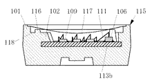
101・・・第一の側壁、
102・・・第二の側壁、
103・・・第三の側壁、
104・・・切欠部、
105a・・・第一の壁部、
105b・・・第二の壁部、
106・・・保護素子、
107・・・接着材、
108・・・溝部、
109・・・発光素子、
110・・・導電性接着材、
111・・・導電性ワイヤ、
112・・・厚肉部、
113a・・・正のリード電極、
113b・・・負のリード電極、
114・・・段差、
115・・・支持部、
116・・・突出部、
117・・・封止部材、
118・・・突出部116と第一の側壁101との間の底面、
119・・・凹部。
Claims (3)
- 発光素子と、
リード電極と、そのリード電極を保持する支持部と、を有する支持体と、
前記発光素子および前記リード電極を接続する導電性ワイヤと、
前記発光素子を被覆し前記支持部により設けられた凹部内に配置されかつ前記凹部を充填してなる封止部材と、
を備えた半導体装置であって、
前記支持部は、前記凹部の開口部を形成する第一の側壁と、その第一の側壁に接続し、かつ、前記リード電極の主面の一部上まで前記凹部内を内側方向に延在して設けられた第二の側壁と、さらに、前記凹部底面における正負一対のリード電極の端部間において、または、前記リード電極のうち少なくとも一方の厚さ方向に貫通された孔の上において、前記支持部と接続して前記凹部の底面を横断する壁部と、を有しており、
前記第二の側壁の少なくとも一部が、前記壁部に接続されており、
前記壁部は、前記発光素子の搭載部と、前記リード電極における前記導電性ワイヤの接続部と、の間に設けられており、
前記凹部底面における前記第二の側壁の下部は、前記凹部底面における前記第一の側壁の下部と接続されており、
前記第二の側壁を形成する壁面のうち、前記発光素子の搭載部に最も近い壁面が前記発光素子との間隔が大きくなるように円弧面とされており、
前記封止部材は、シリコーン樹脂、エポキシ樹脂、ユリア樹脂、フッ素樹脂、および、それらの樹脂を少なくとも一種以上含むハイブリッド樹脂等、耐候性に優れた透光性樹脂から選択されることを特徴とする半導体装置。 - 前記支持部は、前記第二の側壁に向かい合う方向に第三の側壁を有しており、前記壁部の両端部が前記第二の側壁および前記第三の側壁にそれぞれ接続されている請求項1に記載の半導体装置。
- 前記支持体は、前記リード電極が突出された支持部の側面において、前記支持部の一部が突出されている請求項1または2に記載の半導体装置。
Priority Applications (1)
| Application Number | Priority Date | Filing Date | Title |
|---|---|---|---|
| JP2006273325A JP5710088B2 (ja) | 2006-10-04 | 2006-10-04 | 半導体装置 |
Applications Claiming Priority (1)
| Application Number | Priority Date | Filing Date | Title |
|---|---|---|---|
| JP2006273325A JP5710088B2 (ja) | 2006-10-04 | 2006-10-04 | 半導体装置 |
Publications (3)
| Publication Number | Publication Date |
|---|---|
| JP2008091792A JP2008091792A (ja) | 2008-04-17 |
| JP2008091792A5 JP2008091792A5 (ja) | 2009-11-19 |
| JP5710088B2 true JP5710088B2 (ja) | 2015-04-30 |
Family
ID=39375606
Family Applications (1)
| Application Number | Title | Priority Date | Filing Date |
|---|---|---|---|
| JP2006273325A Active JP5710088B2 (ja) | 2006-10-04 | 2006-10-04 | 半導体装置 |
Country Status (1)
| Country | Link |
|---|---|
| JP (1) | JP5710088B2 (ja) |
Families Citing this family (10)
| Publication number | Priority date | Publication date | Assignee | Title |
|---|---|---|---|---|
| US8598602B2 (en) | 2009-01-12 | 2013-12-03 | Cree, Inc. | Light emitting device packages with improved heat transfer |
| US7923739B2 (en) | 2009-06-05 | 2011-04-12 | Cree, Inc. | Solid state lighting device |
| US9111778B2 (en) | 2009-06-05 | 2015-08-18 | Cree, Inc. | Light emitting diode (LED) devices, systems, and methods |
| US8860043B2 (en) | 2009-06-05 | 2014-10-14 | Cree, Inc. | Light emitting device packages, systems and methods |
| US20130043502A1 (en) * | 2010-05-31 | 2013-02-21 | Panasonic Corporation | Light emitting device and method for manufacturing the same |
| US8269244B2 (en) | 2010-06-28 | 2012-09-18 | Cree, Inc. | LED package with efficient, isolated thermal path |
| US11101408B2 (en) | 2011-02-07 | 2021-08-24 | Creeled, Inc. | Components and methods for light emitting diode (LED) lighting |
| US8610140B2 (en) | 2010-12-15 | 2013-12-17 | Cree, Inc. | Light emitting diode (LED) packages, systems, devices and related methods |
| KR101110911B1 (ko) * | 2010-12-24 | 2012-02-24 | 엘지이노텍 주식회사 | 발광소자 패키지 |
| TW201251140A (en) | 2011-01-31 | 2012-12-16 | Cree Inc | High brightness light emitting diode (LED) packages, systems and methods with improved resin filling and high adhesion |
Family Cites Families (7)
| Publication number | Priority date | Publication date | Assignee | Title |
|---|---|---|---|---|
| JP3707024B2 (ja) * | 1997-04-17 | 2005-10-19 | 松下電器産業株式会社 | 電子部品 |
| JP2002033520A (ja) * | 2000-07-14 | 2002-01-31 | Toshiba Electronic Engineering Corp | 半導体発光装置 |
| JP3659635B2 (ja) * | 2001-04-10 | 2005-06-15 | 株式会社東芝 | 光半導体装置 |
| JP3991961B2 (ja) * | 2002-09-05 | 2007-10-17 | 日亜化学工業株式会社 | 側面発光型発光装置 |
| TWI237546B (en) * | 2003-01-30 | 2005-08-01 | Osram Opto Semiconductors Gmbh | Semiconductor-component sending and/or receiving electromagnetic radiation and housing-basebody for such a component |
| JP2004193537A (ja) * | 2003-02-21 | 2004-07-08 | Nichia Chem Ind Ltd | 発光装置およびそれを用いた面状光源 |
| JP4645071B2 (ja) * | 2003-06-20 | 2011-03-09 | 日亜化学工業株式会社 | パッケージ成型体およびそれを用いた半導体装置 |
-
2006
- 2006-10-04 JP JP2006273325A patent/JP5710088B2/ja active Active
Also Published As
| Publication number | Publication date |
|---|---|
| JP2008091792A (ja) | 2008-04-17 |
Similar Documents
| Publication | Publication Date | Title |
|---|---|---|
| JP5710088B2 (ja) | 半導体装置 | |
| US10374136B2 (en) | Light emitting apparatus | |
| JP5333237B2 (ja) | 発光装置 | |
| JP5453713B2 (ja) | 半導体装置およびその形成方法 | |
| JP5233170B2 (ja) | 発光装置、発光装置を構成する樹脂成形体及びそれらの製造方法 | |
| EP2315263B1 (en) | Light-emitting device | |
| US9112124B2 (en) | Light emitting device | |
| JP5994472B2 (ja) | 発光装置 | |
| JP5034686B2 (ja) | 半導体装置 | |
| JP5444654B2 (ja) | 発光装置 | |
| US9281460B2 (en) | Light emitting device package and light emitting device having lead-frames | |
| JP6523597B2 (ja) | 発光装置 | |
| TW201203632A (en) | Light emitting device | |
| JP6947995B2 (ja) | 発光装置 | |
| JP6225910B2 (ja) | 発光装置 | |
| JP5233619B2 (ja) | 半導体装置 | |
| JP5233478B2 (ja) | 発光装置 | |
| JP2004165308A (ja) | 発光装置 | |
| JP2009055066A (ja) | 発光装置 | |
| JP4967551B2 (ja) | 発光装置 | |
| JP6402890B2 (ja) | 発光装置およびその製造方法 |
Legal Events
| Date | Code | Title | Description |
|---|---|---|---|
| A521 | Request for written amendment filed |
Free format text: JAPANESE INTERMEDIATE CODE: A523 Effective date: 20091002 |
|
| A621 | Written request for application examination |
Free format text: JAPANESE INTERMEDIATE CODE: A621 Effective date: 20091002 |
|
| A131 | Notification of reasons for refusal |
Free format text: JAPANESE INTERMEDIATE CODE: A131 Effective date: 20110906 |
|
| A977 | Report on retrieval |
Free format text: JAPANESE INTERMEDIATE CODE: A971007 Effective date: 20110907 |
|
| A521 | Request for written amendment filed |
Free format text: JAPANESE INTERMEDIATE CODE: A523 Effective date: 20111107 |
|
| A131 | Notification of reasons for refusal |
Free format text: JAPANESE INTERMEDIATE CODE: A131 Effective date: 20120522 |
|
| A131 | Notification of reasons for refusal |
Free format text: JAPANESE INTERMEDIATE CODE: A131 Effective date: 20130219 |
|
| A521 | Request for written amendment filed |
Free format text: JAPANESE INTERMEDIATE CODE: A523 Effective date: 20130422 |
|
| A02 | Decision of refusal |
Free format text: JAPANESE INTERMEDIATE CODE: A02 Effective date: 20130820 |
|
| A521 | Request for written amendment filed |
Free format text: JAPANESE INTERMEDIATE CODE: A523 Effective date: 20141208 |
|
| A521 | Request for written amendment filed |
Free format text: JAPANESE INTERMEDIATE CODE: A523 Effective date: 20150127 |
|
| A61 | First payment of annual fees (during grant procedure) |
Free format text: JAPANESE INTERMEDIATE CODE: A61 Effective date: 20150304 |
|
| R150 | Certificate of patent or registration of utility model |
Ref document number: 5710088 Country of ref document: JP Free format text: JAPANESE INTERMEDIATE CODE: R150 |
|
| R250 | Receipt of annual fees |
Free format text: JAPANESE INTERMEDIATE CODE: R250 |
|
| R250 | Receipt of annual fees |
Free format text: JAPANESE INTERMEDIATE CODE: R250 |
|
| R250 | Receipt of annual fees |
Free format text: JAPANESE INTERMEDIATE CODE: R250 |
|
| R250 | Receipt of annual fees |
Free format text: JAPANESE INTERMEDIATE CODE: R250 |
|
| R250 | Receipt of annual fees |
Free format text: JAPANESE INTERMEDIATE CODE: R250 |
|
| R250 | Receipt of annual fees |
Free format text: JAPANESE INTERMEDIATE CODE: R250 |