JP5663379B2 - 接続端子構造及びソケット並びに電子部品パッケージ - Google Patents
接続端子構造及びソケット並びに電子部品パッケージ Download PDFInfo
- Publication number
- JP5663379B2 JP5663379B2 JP2011087156A JP2011087156A JP5663379B2 JP 5663379 B2 JP5663379 B2 JP 5663379B2 JP 2011087156 A JP2011087156 A JP 2011087156A JP 2011087156 A JP2011087156 A JP 2011087156A JP 5663379 B2 JP5663379 B2 JP 5663379B2
- Authority
- JP
- Japan
- Prior art keywords
- connection terminal
- substrate
- electrode pad
- terminal structure
- semiconductor package
- Prior art date
- Legal status (The legal status is an assumption and is not a legal conclusion. Google has not performed a legal analysis and makes no representation as to the accuracy of the status listed.)
- Active
Links
Images


Classifications
-
- H—ELECTRICITY
- H01—ELECTRIC ELEMENTS
- H01R—ELECTRICALLY-CONDUCTIVE CONNECTIONS; STRUCTURAL ASSOCIATIONS OF A PLURALITY OF MUTUALLY-INSULATED ELECTRICAL CONNECTING ELEMENTS; COUPLING DEVICES; CURRENT COLLECTORS
- H01R12/00—Structural associations of a plurality of mutually-insulated electrical connecting elements, specially adapted for printed circuits, e.g. printed circuit boards [PCB], flat or ribbon cables, or like generally planar structures, e.g. terminal strips, terminal blocks; Coupling devices specially adapted for printed circuits, flat or ribbon cables, or like generally planar structures; Terminals specially adapted for contact with, or insertion into, printed circuits, flat or ribbon cables, or like generally planar structures
- H01R12/50—Fixed connections
- H01R12/51—Fixed connections for rigid printed circuits or like structures
- H01R12/52—Fixed connections for rigid printed circuits or like structures connecting to other rigid printed circuits or like structures
-
- H—ELECTRICITY
- H01—ELECTRIC ELEMENTS
- H01R—ELECTRICALLY-CONDUCTIVE CONNECTIONS; STRUCTURAL ASSOCIATIONS OF A PLURALITY OF MUTUALLY-INSULATED ELECTRICAL CONNECTING ELEMENTS; COUPLING DEVICES; CURRENT COLLECTORS
- H01R12/00—Structural associations of a plurality of mutually-insulated electrical connecting elements, specially adapted for printed circuits, e.g. printed circuit boards [PCB], flat or ribbon cables, or like generally planar structures, e.g. terminal strips, terminal blocks; Coupling devices specially adapted for printed circuits, flat or ribbon cables, or like generally planar structures; Terminals specially adapted for contact with, or insertion into, printed circuits, flat or ribbon cables, or like generally planar structures
- H01R12/50—Fixed connections
- H01R12/51—Fixed connections for rigid printed circuits or like structures
- H01R12/55—Fixed connections for rigid printed circuits or like structures characterised by the terminals
- H01R12/57—Fixed connections for rigid printed circuits or like structures characterised by the terminals surface mounting terminals
-
- H—ELECTRICITY
- H01—ELECTRIC ELEMENTS
- H01R—ELECTRICALLY-CONDUCTIVE CONNECTIONS; STRUCTURAL ASSOCIATIONS OF A PLURALITY OF MUTUALLY-INSULATED ELECTRICAL CONNECTING ELEMENTS; COUPLING DEVICES; CURRENT COLLECTORS
- H01R12/00—Structural associations of a plurality of mutually-insulated electrical connecting elements, specially adapted for printed circuits, e.g. printed circuit boards [PCB], flat or ribbon cables, or like generally planar structures, e.g. terminal strips, terminal blocks; Coupling devices specially adapted for printed circuits, flat or ribbon cables, or like generally planar structures; Terminals specially adapted for contact with, or insertion into, printed circuits, flat or ribbon cables, or like generally planar structures
- H01R12/70—Coupling devices
- H01R12/71—Coupling devices for rigid printing circuits or like structures
- H01R12/712—Coupling devices for rigid printing circuits or like structures co-operating with the surface of the printed circuit or with a coupling device exclusively provided on the surface of the printed circuit
- H01R12/714—Coupling devices for rigid printing circuits or like structures co-operating with the surface of the printed circuit or with a coupling device exclusively provided on the surface of the printed circuit with contacts abutting directly the printed circuit; Button contacts therefore provided on the printed circuit
-
- H—ELECTRICITY
- H01—ELECTRIC ELEMENTS
- H01R—ELECTRICALLY-CONDUCTIVE CONNECTIONS; STRUCTURAL ASSOCIATIONS OF A PLURALITY OF MUTUALLY-INSULATED ELECTRICAL CONNECTING ELEMENTS; COUPLING DEVICES; CURRENT COLLECTORS
- H01R12/00—Structural associations of a plurality of mutually-insulated electrical connecting elements, specially adapted for printed circuits, e.g. printed circuit boards [PCB], flat or ribbon cables, or like generally planar structures, e.g. terminal strips, terminal blocks; Coupling devices specially adapted for printed circuits, flat or ribbon cables, or like generally planar structures; Terminals specially adapted for contact with, or insertion into, printed circuits, flat or ribbon cables, or like generally planar structures
- H01R12/70—Coupling devices
- H01R12/71—Coupling devices for rigid printing circuits or like structures
- H01R12/712—Coupling devices for rigid printing circuits or like structures co-operating with the surface of the printed circuit or with a coupling device exclusively provided on the surface of the printed circuit
- H01R12/716—Coupling device provided on the PCB
-
- H—ELECTRICITY
- H01—ELECTRIC ELEMENTS
- H01R—ELECTRICALLY-CONDUCTIVE CONNECTIONS; STRUCTURAL ASSOCIATIONS OF A PLURALITY OF MUTUALLY-INSULATED ELECTRICAL CONNECTING ELEMENTS; COUPLING DEVICES; CURRENT COLLECTORS
- H01R13/00—Details of coupling devices of the kinds covered by groups H01R12/70 or H01R24/00 - H01R33/00
- H01R13/02—Contact members
- H01R13/22—Contacts for co-operating by abutting
- H01R13/24—Contacts for co-operating by abutting resilient; resiliently-mounted
- H01R13/2442—Contacts for co-operating by abutting resilient; resiliently-mounted with a single cantilevered beam
-
- H—ELECTRICITY
- H05—ELECTRIC TECHNIQUES NOT OTHERWISE PROVIDED FOR
- H05K—PRINTED CIRCUITS; CASINGS OR CONSTRUCTIONAL DETAILS OF ELECTRIC APPARATUS; MANUFACTURE OF ASSEMBLAGES OF ELECTRICAL COMPONENTS
- H05K7/00—Constructional details common to different types of electric apparatus
- H05K7/02—Arrangements of circuit components or wiring on supporting structure
- H05K7/10—Plug-in assemblages of components, e.g. IC sockets
- H05K7/1053—Plug-in assemblages of components, e.g. IC sockets having interior leads
- H05K7/1061—Plug-in assemblages of components, e.g. IC sockets having interior leads co-operating by abutting
- H05K7/1069—Plug-in assemblages of components, e.g. IC sockets having interior leads co-operating by abutting with spring contact pieces
Description
又、本接続端子構造の他の形態は、第7面及び前記第7面の反対面である第8面を備えた第1補強板と、第9面及び前記第9面の反対面である第10面を備えた第2補強板と、前記第1補強板の第8面と前記第2補強板の第9面との間に設けられ、前記第1補強板と前記第2補強板と接触して前記第1補強板と前記第2補強板とを接合する支持体と、第5面及び前記第5面の反対面である第6面を備え、前記第6面の一端側が前記第1補強板の第7面と接合され、前記第6面の他端側が前記第2補強板の第10面と接合されたフレキシブル基板と、前記フレキシブル基板の第5面の一端側に形成された第1電極パッドと、前記フレキシブル基板の第5面の他端側に形成され、前記第1電極パッドと電気的に接続された第4電極パッドと、前記第1電極パッド及び前記第4電極パッドの少なくとも一方と接合された接続端子と、を有することを要件とする。
[第1の実施の形態に係る接続端子構造]
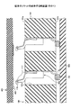
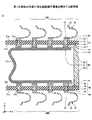
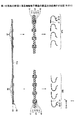
図3は、第1の実施の形態に係る接続端子構造を例示する斜視図である。図4は、第1の実施の形態に係る接続端子構造を例示する分解斜視図である。図5は、第1の実施の形態に係る接続端子構造を例示する断面図である。図6は、第1の実施の形態に係る接続端子構造を例示する平面図である。なお、図5は、図6の各接続端子30の配設方向Cに平行な断面を示している。但し、図6に示すように、平面視において各接続端子30は配設方向Cに対して傾いているため、配設方向Cに平行な断面図では接続端子30の断面形状を示すことができない。そこで、便宜上、図5では、配設方向Cに対してθ1傾斜した方向に平行な接続端子30の断面形状を模式的に示している(以降の断面図でも同様)。
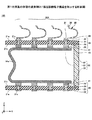
次に、図8〜図10を参照しながら、接続端子構造10の製造方法について説明する。図8〜図10は、第1の実施の形態に係る接続端子構造の製造方法を例示する図である。なお、図8において、基板20等は図5等とは上下が反転した状態で描かれている。
第1の実施の形態の変形例1では、フレキシブル基板の裏側に補強板を設ける例を示す。なお、第1の実施の形態の変形例1において、既に説明した実施の形態と同一構成部品についての説明は省略する。
第1の実施の形態の変形例2では、支持体の一方の側のみに接続端子群を設ける例を示す。なお、第1の実施の形態の変形例2において、既に説明した実施の形態と同一構成部品についての説明は省略する。
第1の実施の形態の変形例3では、第1の実施の形態とは平面形状の異なる接続端子構造の例を示す。なお、第1の実施の形態の変形例3において、既に説明した実施の形態と同一構成部品についての説明は省略する。
第2の実施の形態では、第1の実施の形態の変形例3に係る接続端子構造10Cを用いて半導体パッケージの電気的な検査を行う例を示す。なお、第2の実施の形態において、既に説明した実施の形態と同一構成部品についての説明は省略する。
第2の実施の形態の変形例1では、第1の実施の形態の変形例3に係る接続端子構造10Cを用いて、第2の実施の形態とは異なる半導体パッケージの電気的な検査を行う例を示す。なお、第2の実施の形態の変形例1において、既に説明した実施の形態と同一構成部品についての説明は省略する。
第2の実施の形態の変形例2では、第1の実施の形態の変形例3に係る接続端子構造10Cを用いて、第2の実施の形態及びその変形例1とは異なる半導体パッケージの電気的な検査を行う例を示す。なお、第2の実施の形態の変形例2において、既に説明した実施の形態と同一構成部品についての説明は省略する。
第3の実施の形態では、第1の実施の形態の変形例3に係る接続端子構造10Cを構成要素とする電子部品パッケージの例を示す。なお、第3の実施の形態において、既に説明した実施の形態と同一構成部品についての説明は省略する。
20、20A、61 基板
21、21A、51、71、91 基板本体
21x 貫通孔
21y、51x、51y 開口部
22、23、52、53、64、65、72、92、93 電極パッド
24 貫通配線
25 補強板
30 接続端子
30A、30B、30C、30D 接続端子群
31 固定部
31a、34a 面
32 接続部
33 ばね部
34 第1支持部
35 第2支持部
38 当接部
39 突出部
40、41、43、44、94、95 接合部
44a コア部
44b はんだ
50、50A フレキシブル基板
55、57 支持体
55a 上端面
55b 下端面
60A、60B、60C、60D、60E、100、100A、100B 半導体パッケージ
62、67 半導体チップ
63、68 封止樹脂
69 電子部品
70 検査用基板
80、80A 筐体
81、87 枠部
81a、87a 上面
82、88 蓋部
83、84、85、86 位置決め保持部
83a、83b、84a、84b、85a、85b、86a、86b 面
90 中継基板
100C 電子部品パッケージ
C 配設方向
L、R 領域
θ1、θ2 角度
Claims (14)
- 第1面及び前記第1面の反対面である第2面を備えた第1基板と、
前記第1基板の第1面に形成された第1電極パッドと、
前記第1基板の第2面に形成された第2電極パッドと、
第3面及び前記第3面の反対面である第4面を備えた第2基板と、
前記第2基板の第3面に形成された第3電極パッドと、
前記第2基板の第4面に形成された第4電極パッドと、
前記第1基板の第2面と前記第2基板の第3面との間に設けられ、前記第1基板の第2面の外縁部と前記第2基板の第3面の外縁部と接触して前記第1基板と前記第2基板とを接合する支持体と、
前記支持体の内側に形成された前記第1基板の第2電極パッドと前記第2基板の第3電極パッドとを電気的に接続するフレキシブル基板と、
前記第1電極パッド及び前記第4電極パッドの少なくとも一方と接合された接続端子と、を有する接続端子構造。 - 第7面及び前記第7面の反対面である第8面を備えた第1補強板と、
第9面及び前記第9面の反対面である第10面を備えた第2補強板と、
前記第1補強板の第8面と前記第2補強板の第9面との間に設けられ、前記第1補強板と前記第2補強板と接触して前記第1補強板と前記第2補強板とを接合する支持体と、
第5面及び前記第5面の反対面である第6面を備え、前記第6面の一端側が前記第1補強板の第7面と接合され、前記第6面の他端側が前記第2補強板の第10面と接合されたフレキシブル基板と、
前記フレキシブル基板の第5面の一端側に形成された第1電極パッドと、
前記フレキシブル基板の第5面の他端側に形成され、前記第1電極パッドと電気的に接続された第4電極パッドと、
前記第1電極パッド及び前記第4電極パッドの少なくとも一方と接合された接続端子と、を有する接続端子構造。 - 前記フレキシブル基板の第5面の一端側に形成された第5電極パッドと、
前記フレキシブル基板の第5面の他端側に形成された第6電極パッドと、を有し、
前記第5電極パッドは前記第2電極パッドと接続され、
前記第6電極パッドは前記第3電極パッドと接続されている請求項1記載の接続端子構造。 - 前記フレキシブル基板は、前記一端側と前記他端側との間で折り曲げられている請求項2又は3記載の接続端子構造。
- 前記支持体は平面形状がコの字型である請求項1又は3記載の接続端子構造。
- 前記接続端子は、ばね性を有する導電性の部材である請求項1乃至5の何れか一項記載の接続端子構造。
- 前記接続端子は、
前記接続端子の一端に形成された固定部と、
前記接続端子の他端に形成され、前記固定部と対向するように配置された接続部と、
前記固定部と前記接続部との間に配置されており、前記固定部と前記接続部と一体的に形成された、ばね性を有する湾曲した形状のばね部と、を有し、
前記固定部は前記第1電極パッド及び前記第4電極パッドの少なくとも一方と接合されている請求項1乃至6の何れか一項記載の接続端子構造。 - 前記第1電極パッド側から前記第4電極パッド側に貫通する開口部を有する請求項1乃至7の何れか一項記載の接続端子構造。
- 請求項1乃至8の何れか一項記載の接続端子構造を有し、前記接続端子構造を介して被接続物を着脱可能な状態で他の被接続物に接続するソケット。
- 前記接続端子構造、前記被接続物、及び前記他の被接続物を位置決めする枠部が設けられている請求項9記載のソケット。
- 前記接続端子構造は、前記第1電極パッド側から前記第4電極パッド側に貫通する開口部を有し、
電子部品が実装された前記被接続物及び電子部品が実装された前記他の被接続物を接続する際には、前記被接続物に実装された電子部品、前記他の被接続物に実装された電子部品の何れか一方又は双方が前記開口部内に配置される請求項9又は10記載のソケット。 - 被接続物と、請求項1乃至8の何れか一項記載の接続端子構造、及び他の被接続物を有し、前記被接続物と前記他の被接続物とが前記接続端子構造を介して電気的に接続されている電子部品パッケージ。
- 前記被接続物、前記接続端子構造、及び前記他の被接続物を位置決めする枠部が設けられている請求項12記載の電子部品パッケージ。
- 前記接続端子構造は、前記第1電極パッド側から前記第4電極パッド側に貫通する開口部を有し、
前記被接続物及び前記他の被接続物には、それぞれ電子部品が実装されており、
前記被接続物に実装された電子部品、前記他の被接続物に実装された電子部品の何れか一方又は双方が前記開口部内に配置されている請求項12又は13記載の電子部品パッケージ。
Priority Applications (2)
| Application Number | Priority Date | Filing Date | Title |
|---|---|---|---|
| JP2011087156A JP5663379B2 (ja) | 2011-04-11 | 2011-04-11 | 接続端子構造及びソケット並びに電子部品パッケージ |
| US13/433,841 US8708711B2 (en) | 2011-04-11 | 2012-03-29 | Connecting terminal structure, socket and electronic package |
Applications Claiming Priority (1)
| Application Number | Priority Date | Filing Date | Title |
|---|---|---|---|
| JP2011087156A JP5663379B2 (ja) | 2011-04-11 | 2011-04-11 | 接続端子構造及びソケット並びに電子部品パッケージ |
Publications (3)
| Publication Number | Publication Date |
|---|---|
| JP2012221783A JP2012221783A (ja) | 2012-11-12 |
| JP2012221783A5 JP2012221783A5 (ja) | 2014-03-20 |
| JP5663379B2 true JP5663379B2 (ja) | 2015-02-04 |
Family
ID=46966453
Family Applications (1)
| Application Number | Title | Priority Date | Filing Date |
|---|---|---|---|
| JP2011087156A Active JP5663379B2 (ja) | 2011-04-11 | 2011-04-11 | 接続端子構造及びソケット並びに電子部品パッケージ |
Country Status (2)
| Country | Link |
|---|---|
| US (1) | US8708711B2 (ja) |
| JP (1) | JP5663379B2 (ja) |
Families Citing this family (11)
| Publication number | Priority date | Publication date | Assignee | Title |
|---|---|---|---|---|
| JP2014071964A (ja) * | 2012-09-27 | 2014-04-21 | Fujitsu Component Ltd | コンタクト部材 |
| JP6011574B2 (ja) * | 2013-06-27 | 2016-10-19 | 株式会社村田製作所 | 積層セラミックコンデンサ |
| WO2016048352A1 (en) * | 2014-09-26 | 2016-03-31 | Intel Corporation | Socket contact techniques and configurations |
| US9515401B1 (en) * | 2016-01-04 | 2016-12-06 | International Business Machines Corporation | Elastomeric electrical connector structure joining two hardware planes at right angles to each other |
| US10559902B2 (en) | 2016-01-04 | 2020-02-11 | International Business Machines Corporation | Electrical connection management using a card |
| CN206532926U (zh) * | 2017-01-18 | 2017-09-29 | 番禺得意精密电子工业有限公司 | 电连接器 |
| CN206685558U (zh) * | 2017-04-01 | 2017-11-28 | 番禺得意精密电子工业有限公司 | 电连接器 |
| CN107968284B (zh) * | 2017-09-11 | 2020-06-09 | 番禺得意精密电子工业有限公司 | 电连接器 |
| CN110649445B (zh) * | 2018-06-27 | 2021-02-26 | 欣兴电子股份有限公司 | 连接器结构的制作方法 |
| JP6832313B2 (ja) * | 2018-07-23 | 2021-02-24 | 矢崎総業株式会社 | フレキシブルプリント配線板のコネクタ取付構造 |
| CN113130432B (zh) * | 2019-12-30 | 2022-12-27 | 华为机器有限公司 | 一种电子模块及电子设备 |
Family Cites Families (13)
| Publication number | Priority date | Publication date | Assignee | Title |
|---|---|---|---|---|
| DE2234960C3 (de) * | 1971-11-26 | 1975-04-30 | Teledyne, Inc., Los Angeles, Calif. (V.St.A.) | Elektrischer Stecker |
| JPS61138181U (ja) * | 1985-02-16 | 1986-08-27 | ||
| US20070020960A1 (en) * | 2003-04-11 | 2007-01-25 | Williams John D | Contact grid array system |
| CN101156506B (zh) * | 2005-07-11 | 2011-07-13 | 松下电器产业株式会社 | 基板连接部件和连接结构体 |
| US7845954B2 (en) * | 2005-07-14 | 2010-12-07 | Panasonic Corporation | Interconnecting board and three-dimensional wiring structure using it |
| CN100440628C (zh) * | 2005-10-17 | 2008-12-03 | 富士康(昆山)电脑接插件有限公司 | 电连接器 |
| US7438557B1 (en) * | 2007-11-13 | 2008-10-21 | International Business Machines Corporation | Stacked multiple electronic component interconnect structure |
| US7766667B2 (en) * | 2007-12-18 | 2010-08-03 | Russell James V | Separable electrical connectors using isotropic conductive elastomer interconnect medium |
| WO2009091958A1 (en) * | 2008-01-17 | 2009-07-23 | Amphenol Corporation | Interposer assembly and method |
| JP5606695B2 (ja) * | 2009-07-03 | 2014-10-15 | 新光電気工業株式会社 | 接続端子付き基板 |
| US8123529B2 (en) * | 2009-12-18 | 2012-02-28 | International Business Machines Corporation | Apparatus for connecting two area array devices using a printed circuit board with holes with conductors electrically connected to each other |
| JP2011258364A (ja) * | 2010-06-08 | 2011-12-22 | Shinko Electric Ind Co Ltd | ソケット |
| US8133061B1 (en) * | 2010-11-29 | 2012-03-13 | International Business Machines Corporation | Removable and replaceable dual-sided connector pin interposer |
-
2011
- 2011-04-11 JP JP2011087156A patent/JP5663379B2/ja active Active
-
2012
- 2012-03-29 US US13/433,841 patent/US8708711B2/en active Active
Also Published As
| Publication number | Publication date |
|---|---|
| US8708711B2 (en) | 2014-04-29 |
| JP2012221783A (ja) | 2012-11-12 |
| US20120258636A1 (en) | 2012-10-11 |
Similar Documents
| Publication | Publication Date | Title |
|---|---|---|
| JP5663379B2 (ja) | 接続端子構造及びソケット並びに電子部品パッケージ | |
| JP5713598B2 (ja) | ソケット及びその製造方法 | |
| KR101171842B1 (ko) | 초미세 피치의 적층을 갖는 마이크로전자 조립체 | |
| JP5582995B2 (ja) | ソケット | |
| US7129420B2 (en) | Semiconductor device and method for manufacture thereof, circuit board, and electronic instrument | |
| JP5500870B2 (ja) | 接続端子付き基板及び電子部品のソケット等 | |
| JP5606695B2 (ja) | 接続端子付き基板 | |
| JP5788166B2 (ja) | 接続端子構造及びその製造方法、並びにソケット | |
| WO2001008223A1 (fr) | Dispositif a semiconducteur, son procede de fabrication, carte de circuit imprime et dispositif electronique | |
| US20080150101A1 (en) | Microelectronic packages having improved input/output connections and methods therefor | |
| JP2011258364A (ja) | ソケット | |
| US7315086B2 (en) | Chip-on-board package having flip chip assembly structure and manufacturing method thereof | |
| KR20110128227A (ko) | 다층 프린트 기판 및 그 제조 방법 | |
| KR20090037811A (ko) | 배선 기판 | |
| US7759795B2 (en) | Printed circuit board having reliable bump interconnection structure, method of fabricating the same, and semiconductor package using the same | |
| JP5794833B2 (ja) | 接続端子及びその製造方法、並びにソケット | |
| JP4360240B2 (ja) | 半導体装置と半導体装置用多層基板 | |
| US8083529B2 (en) | Socket | |
| JP2005340393A (ja) | 小型実装モジュール及びその製造方法 | |
| JP2000241500A (ja) | 半導体装置用ソケットの取付構造 | |
| JP2000150577A (ja) | 配線基板とその製造方法、半導体装置、これらを用いた電気部品とその製造方法 | |
| JP2007012748A (ja) | 積層型半導体装置およびその製造方法 | |
| JP4562006B2 (ja) | 半導体装置及びその製造方法、回路基板並びに電子機器 | |
| US20090189272A1 (en) | Wafer Level Chip Scale Packages Including Redistribution Substrates and Methods of Fabricating the Same | |
| TWI395529B (zh) | 載板及其製作方法 |
Legal Events
| Date | Code | Title | Description |
|---|---|---|---|
| A521 | Written amendment |
Free format text: JAPANESE INTERMEDIATE CODE: A523 Effective date: 20140131 |
|
| A621 | Written request for application examination |
Free format text: JAPANESE INTERMEDIATE CODE: A621 Effective date: 20140131 |
|
| TRDD | Decision of grant or rejection written | ||
| A977 | Report on retrieval |
Free format text: JAPANESE INTERMEDIATE CODE: A971007 Effective date: 20141128 |
|
| A01 | Written decision to grant a patent or to grant a registration (utility model) |
Free format text: JAPANESE INTERMEDIATE CODE: A01 Effective date: 20141202 |
|
| A61 | First payment of annual fees (during grant procedure) |
Free format text: JAPANESE INTERMEDIATE CODE: A61 Effective date: 20141208 |
|
| R150 | Certificate of patent or registration of utility model |
Ref document number: 5663379 Country of ref document: JP Free format text: JAPANESE INTERMEDIATE CODE: R150 |