JP5645543B2 - 撮像装置 - Google Patents
撮像装置 Download PDFInfo
- Publication number
- JP5645543B2 JP5645543B2 JP2010185421A JP2010185421A JP5645543B2 JP 5645543 B2 JP5645543 B2 JP 5645543B2 JP 2010185421 A JP2010185421 A JP 2010185421A JP 2010185421 A JP2010185421 A JP 2010185421A JP 5645543 B2 JP5645543 B2 JP 5645543B2
- Authority
- JP
- Japan
- Prior art keywords
- amplifier
- signal
- source
- voltage
- mos transistor
- Prior art date
- Legal status (The legal status is an assumption and is not a legal conclusion. Google has not performed a legal analysis and makes no representation as to the accuracy of the status listed.)
- Expired - Fee Related
Links
- 238000003384 imaging method Methods 0.000 title claims description 16
- 239000003990 capacitor Substances 0.000 claims description 66
- 238000006243 chemical reaction Methods 0.000 claims description 6
- 101100495267 Saccharomyces cerevisiae (strain ATCC 204508 / S288c) CDC25 gene Proteins 0.000 description 23
- 238000010586 diagram Methods 0.000 description 18
- 230000007704 transition Effects 0.000 description 9
- 230000000875 corresponding effect Effects 0.000 description 6
- 230000003321 amplification Effects 0.000 description 2
- 238000003199 nucleic acid amplification method Methods 0.000 description 2
- 238000005070 sampling Methods 0.000 description 2
- 101710155594 Coiled-coil domain-containing protein 115 Proteins 0.000 description 1
- 102100035027 Cytosolic carboxypeptidase 1 Human genes 0.000 description 1
- 102100025721 Cytosolic carboxypeptidase 2 Human genes 0.000 description 1
- 101000932634 Homo sapiens Cytosolic carboxypeptidase 2 Proteins 0.000 description 1
- 101001033011 Mus musculus Granzyme C Proteins 0.000 description 1
- 238000003491 array Methods 0.000 description 1
- 230000002596 correlated effect Effects 0.000 description 1
- 230000003247 decreasing effect Effects 0.000 description 1
- 238000007599 discharging Methods 0.000 description 1
- 230000005669 field effect Effects 0.000 description 1
- 238000000034 method Methods 0.000 description 1
- 230000010355 oscillation Effects 0.000 description 1
Images


Classifications
-
- G—PHYSICS
- G11—INFORMATION STORAGE
- G11C—STATIC STORES
- G11C27/00—Electric analogue stores, e.g. for storing instantaneous values
- G11C27/02—Sample-and-hold arrangements
- G11C27/024—Sample-and-hold arrangements using a capacitive memory element
- G11C27/026—Sample-and-hold arrangements using a capacitive memory element associated with an amplifier
-
- G—PHYSICS
- G01—MEASURING; TESTING
- G01J—MEASUREMENT OF INTENSITY, VELOCITY, SPECTRAL CONTENT, POLARISATION, PHASE OR PULSE CHARACTERISTICS OF INFRARED, VISIBLE OR ULTRAVIOLET LIGHT; COLORIMETRY; RADIATION PYROMETRY
- G01J1/00—Photometry, e.g. photographic exposure meter
- G01J1/42—Photometry, e.g. photographic exposure meter using electric radiation detectors
- G01J1/44—Electric circuits
- G01J1/46—Electric circuits using a capacitor
Description
図1は、本発明の第1の実施形態によるサンプルホールド回路の構成例を示す図であり、図2はそのサンプルホールド回路のタイミング図である。図中、Aは、スイッチSとホールド容量Chで形成されるサンプルホールド回路の入力を駆動するバッファーアンプであり、I1はバッファーアンプAのバイアス電流源、VinはバッファーアンプAの入力に印加される信号源である。バッファーアンプCは、信号源Vinの信号を増幅する。ホールド容量Chは、信号を蓄積する。スイッチSは、バッファーアンプAの出力端子及びホールド容量Chの間に接続される。
ωz≒−1/Cc(1/gm− Rc) (3)
(5)
図3は、本発明の第2の実施形態によるサンプルホールド回路の構成例を示す図である。本実施形態は、図1と同様であるが、バッファーアンプAに搭載される位相補償容量(又は帯域制限のための容量)Ccに直列に、サンプルモード、ホールドモードのタイミングに応じて可変できる可変抵抗Rcを接続し、電流源I1を削除している点が異なる。バッファーアンプAは、容量Cc及び可変抵抗Rcの直列接続回路を有する位相補償回路542(図5)を有する負帰還アンプである。抵抗Rcの値を、図4のタイミング図のようにスイッチSがオンしてサンプルモードになっているある期間に、可変抵抗Rcを高抵抗に設定し、該バッファーアンプAを広帯域、高速モードにする。その後、容量Chの端子間電圧の遷移が終了するところで抵抗Rcを低い値に設定し、バッファーアンプAを狭帯域、低ノイズモードにする。上記回路動作によってサンプルホールド回路を高速、低ノイズで動作させることが可能になる。以上のように、可変抵抗Rcを第1の抵抗値(高抵抗)にすることにより第1の信号帯域幅(広帯域)で増幅し、可変抵抗Rcを第1の抵抗値(高抵抗)より低い第2の抵抗値(低抵抗)にすることにより第2の信号帯域幅(狭帯域)で増幅する。
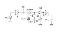
図7は、本発明の第3の実施形態によるバッファーアンプAの構成例を示す図である。本実施形態のバッファーアンプAは、図1のバッファーアンプA及び電流源I1の代わりに設けられる。バッファーアンプAがNMOSソースフォロワーアンプであり、負帰還を掛けた演算増幅器ではない場合である。まず図7を用いて簡単に説明する。図中、M7はソースフォロワーアンプを構成するMOSトランジスタ、I4はMOSトランジスタM7のバイアス電流源、C2は出力負荷容量である。M8はMOSトランジスタ、VAはMOSトランジスタM8のゲートを駆動する電圧源、C3は容量である。
gm=√(2k×Id×W/L) (7)
図8は、本発明の第4の実施形態によるバッファーアンプを説明する図である。本実施形態では、図7内のMOSトランジスタM8と、MOSトランジスタM8のゲートを駆動する電圧源VA、容量C3を用いることで、ソースフォロワーアンプの帯域を制御することが可能になる。前述と同様にして、サンプルホールド回路のスイッチSがオン→オフするタイミングの前後にソースフォロワーアンプの信号帯域幅を変化させることで、サンプルホールドの高速化と低ノイズ化の両立が可能になる。
ωz = 1/(C3×R3) (11)
図14は、本発明の第5の実施形態による撮像装置の構成例を示す図である。第1の実施形態のサンプルホールド回路は、列アンプ部102に適用されている。同図の構成と、その動作タイミングを図15も併用して簡単に説明する。なお、図14では、画素部101は1つしか記載されていないが、2次元的に複数配列された形式のものも当然含まれる。
アンプCを高速モードから低ノイズモードへ変化させる手段は、上記手段以外に第2の実施形態で示した、アンプC内の位相補償容量に直列に接続された抵抗Rcを変化させる方法も当然用いることができる。
Claims (5)
- 各々が光電変換素子を有し、行列状に配列される複数の画素と、
前記複数の画素の各列に対応して設けられ、前記画素の信号を増幅する複数のアンプと、
信号を蓄積する複数のホールド容量と、
前記複数のアンプの出力端子及び前記複数のホールド容量の間にそれぞれ接続される複数のスイッチとを有し、
前記複数のアンプは、それぞれ、1つのオペアンプを有し、
前記複数のアンプの出力端子に対してそれぞれ前記1つのオペアンプの出力端子のみが接続され、
前記各列のアンプは、並列に動作し、
前記スイッチがオンの状態で前記アンプは第1の信号帯域幅で増幅し、その後、前記スイッチがオンの状態で前記アンプは前記第1の信号帯域幅より狭い第2の信号帯域幅で増幅し、その後、前記スイッチがオフの状態で前記アンプは第2の信号帯域幅で増幅することを特徴とする撮像装置。 - 前記アンプは、第1のバイアス電流の供給を受けることにより前記第1の信号帯域幅で増幅し、前記第1のバイアス電流より小さい第2のバイアス電流の供給を受けることにより前記第2の信号帯域幅で増幅することを特徴とする請求項1記載の撮像装置。
- 前記アンプは、容量及び可変抵抗の直列接続回路を有する位相補償回路を有する負帰還アンプであり、前記可変抵抗を第1の抵抗値にすることにより前記第1の信号帯域幅で増幅し、前記可変抵抗を前記第1の抵抗値より低い第2の抵抗値にすることにより前記第2の信号帯域幅で増幅することを特徴とする請求項1記載の撮像装置。
- 前記アンプは、負帰還アンプであることを特徴とする請求項1又は2記載の撮像装置。
- 前記アンプは、ソースフォロワーアンプであることを特徴とする請求項1又は2記載の撮像装置。
Priority Applications (2)
| Application Number | Priority Date | Filing Date | Title |
|---|---|---|---|
| JP2010185421A JP5645543B2 (ja) | 2010-08-20 | 2010-08-20 | 撮像装置 |
| US13/205,836 US20120043454A1 (en) | 2010-08-20 | 2011-08-09 | Sampling and holding circuit, method of driving the same and imaging apparatus |
Applications Claiming Priority (1)
| Application Number | Priority Date | Filing Date | Title |
|---|---|---|---|
| JP2010185421A JP5645543B2 (ja) | 2010-08-20 | 2010-08-20 | 撮像装置 |
Publications (3)
| Publication Number | Publication Date |
|---|---|
| JP2012044549A JP2012044549A (ja) | 2012-03-01 |
| JP2012044549A5 JP2012044549A5 (ja) | 2013-09-19 |
| JP5645543B2 true JP5645543B2 (ja) | 2014-12-24 |
Family
ID=45593310
Family Applications (1)
| Application Number | Title | Priority Date | Filing Date |
|---|---|---|---|
| JP2010185421A Expired - Fee Related JP5645543B2 (ja) | 2010-08-20 | 2010-08-20 | 撮像装置 |
Country Status (2)
| Country | Link |
|---|---|
| US (1) | US20120043454A1 (ja) |
| JP (1) | JP5645543B2 (ja) |
Families Citing this family (12)
| Publication number | Priority date | Publication date | Assignee | Title |
|---|---|---|---|---|
| JP2015080178A (ja) * | 2013-10-18 | 2015-04-23 | キヤノン株式会社 | 撮像素子、撮像装置、カメラ、および、撮像装置の駆動方法 |
| JP6300488B2 (ja) | 2013-10-22 | 2018-03-28 | キヤノン株式会社 | 撮像装置、固体撮像素子及びカメラ |
| US9231525B2 (en) * | 2014-02-28 | 2016-01-05 | Google Inc. | Compensating a two stage amplifier |
| JP6391290B2 (ja) | 2014-05-08 | 2018-09-19 | キヤノン株式会社 | 撮像装置 |
| US9979916B2 (en) | 2014-11-21 | 2018-05-22 | Canon Kabushiki Kaisha | Imaging apparatus and imaging system |
| JP6539149B2 (ja) | 2015-08-13 | 2019-07-03 | キヤノン株式会社 | 撮像装置及び撮像システム |
| US10042005B2 (en) * | 2015-08-21 | 2018-08-07 | Yazaki Corporation | Internal resistance calculating device |
| US9900539B2 (en) | 2015-09-10 | 2018-02-20 | Canon Kabushiki Kaisha | Solid-state image pickup element, and image pickup system |
| JP6674219B2 (ja) | 2015-10-01 | 2020-04-01 | キヤノン株式会社 | 固体撮像装置及び撮像システム |
| JP6632421B2 (ja) | 2016-02-22 | 2020-01-22 | キヤノン株式会社 | 固体撮像装置および撮像装置 |
| JP6833531B2 (ja) | 2017-01-30 | 2021-02-24 | キヤノン株式会社 | 固体撮像装置 |
| FR3084545B1 (fr) * | 2018-07-27 | 2021-05-14 | Soc Fr De Detecteurs Infrarouges Sofradir | Dispositif d’echantillonnage avec gestion de la consommation electrique |
Family Cites Families (12)
| Publication number | Priority date | Publication date | Assignee | Title |
|---|---|---|---|---|
| US5892472A (en) * | 1997-06-30 | 1999-04-06 | Harris Corporation | Processor controlled analog-to-digital converter circuit |
| JP3226859B2 (ja) * | 1997-11-17 | 2001-11-05 | 日本電気株式会社 | 撮像装置 |
| US6128039A (en) * | 1999-01-11 | 2000-10-03 | Omnivision Technologies, Inc. | Column amplifier for high fixed pattern noise reduction |
| JP2003060934A (ja) * | 2001-08-13 | 2003-02-28 | Canon Inc | 増幅器の駆動制御装置及びこれを備えた信号処理システム |
| US6803555B1 (en) * | 2001-09-07 | 2004-10-12 | Indigo Systems Corporation | Two-stage auto-zero amplifier circuit for electro-optical arrays |
| US6661283B1 (en) * | 2002-10-03 | 2003-12-09 | National Semiconductor Corporation | Wide gain range and fine gain step programmable gain amplifier with single stage switched capacitor circuit |
| US7132638B2 (en) * | 2004-06-10 | 2006-11-07 | Fairchild Imaging | CCD imaging array with improved charge sensing circuit |
| US7154331B2 (en) * | 2004-06-29 | 2006-12-26 | Intel Corporation | Adapting operational amplifier frequency response respective to closed loop gain |
| JP4961425B2 (ja) * | 2006-11-30 | 2012-06-27 | パナソニック株式会社 | 演算増幅器 |
| US8217328B2 (en) * | 2009-05-05 | 2012-07-10 | Himax Imaging, Inc. | Low noise pixel readout circuit with high conversion gain |
| JP4777451B2 (ja) * | 2009-08-17 | 2011-09-21 | キヤノン株式会社 | 撮像装置 |
| US8471751B2 (en) * | 2011-06-30 | 2013-06-25 | Intel Corporation | Two-stage analog-to-digital converter using SAR and TDC |
-
2010
- 2010-08-20 JP JP2010185421A patent/JP5645543B2/ja not_active Expired - Fee Related
-
2011
- 2011-08-09 US US13/205,836 patent/US20120043454A1/en not_active Abandoned
Also Published As
| Publication number | Publication date |
|---|---|
| JP2012044549A (ja) | 2012-03-01 |
| US20120043454A1 (en) | 2012-02-23 |
Similar Documents
| Publication | Publication Date | Title |
|---|---|---|
| JP5645543B2 (ja) | 撮像装置 | |
| US9143119B2 (en) | Comparator and analog-to-digital converter using the same | |
| US7639073B2 (en) | Switched-capacitor amplifier with improved reset phase | |
| JP5814539B2 (ja) | 撮像装置 | |
| JP6319946B2 (ja) | 固体撮像装置及び撮像システム | |
| JP6317568B2 (ja) | 比較回路およびそれを用いた撮像素子並びに比較回路の制御方法 | |
| JP6351404B2 (ja) | 撮像装置及び撮像システム | |
| CN111434106B (zh) | 固体摄像装置和ab级超源跟随器 | |
| US7746170B2 (en) | Class AB amplifier and imagers and systems using same | |
| US9344652B2 (en) | Photoelectric conversion apparatus and image pickup system including an ad conversion unit to convert a signal into a digital signal | |
| JP2011166792A (ja) | 小型低雑音信号読み出し回路及びその作動方法 | |
| JPWO2013031097A1 (ja) | 固体撮像装置及び撮像装置 | |
| JP6385193B2 (ja) | 固体撮像装置及び撮像システム | |
| JP5735141B2 (ja) | Cmosイメージセンサ画素読み出し回路構造および画素構造 | |
| US7474154B1 (en) | Bias device clamping circuit for fast over-range recovery | |
| US10044964B2 (en) | Column signal processing unit with driving method for photoelectric conversion apparatus, photoelectric conversion apparatus, and image pickup system | |
| US9497398B2 (en) | Solid-state imaging device and camera for reducing random row noise | |
| US10396725B2 (en) | Amplifier and reset method thereof | |
| US9160948B2 (en) | Replica noise generator using pixel modeling and ramp signal generator including the same | |
| JPH10136266A (ja) | 固体撮像装置 | |
| JP2006033815A (ja) | 固体撮像装置 | |
| JP2007028192A (ja) | 固体撮像素子のcds回路 | |
| KR102644012B1 (ko) | 출력 범위 제어 기능을 가지는 증폭기 및 그를 이용한 다단 증폭 장치 | |
| JP2015186069A (ja) | 光電変換装置及びその駆動方法 | |
| JP5001970B2 (ja) | 固体撮像装置 |
Legal Events
| Date | Code | Title | Description |
|---|---|---|---|
| A521 | Request for written amendment filed |
Free format text: JAPANESE INTERMEDIATE CODE: A523 Effective date: 20130809 |
|
| A621 | Written request for application examination |
Free format text: JAPANESE INTERMEDIATE CODE: A621 Effective date: 20130809 |
|
| A977 | Report on retrieval |
Free format text: JAPANESE INTERMEDIATE CODE: A971007 Effective date: 20140212 |
|
| A131 | Notification of reasons for refusal |
Free format text: JAPANESE INTERMEDIATE CODE: A131 Effective date: 20140218 |
|
| A521 | Request for written amendment filed |
Free format text: JAPANESE INTERMEDIATE CODE: A523 Effective date: 20140416 |
|
| TRDD | Decision of grant or rejection written | ||
| A01 | Written decision to grant a patent or to grant a registration (utility model) |
Free format text: JAPANESE INTERMEDIATE CODE: A01 Effective date: 20141007 |
|
| A61 | First payment of annual fees (during grant procedure) |
Free format text: JAPANESE INTERMEDIATE CODE: A61 Effective date: 20141104 |
|
| LAPS | Cancellation because of no payment of annual fees |