JP5551446B2 - 高速の半導体光変調器 - Google Patents
高速の半導体光変調器 Download PDFInfo
- Publication number
- JP5551446B2 JP5551446B2 JP2009551977A JP2009551977A JP5551446B2 JP 5551446 B2 JP5551446 B2 JP 5551446B2 JP 2009551977 A JP2009551977 A JP 2009551977A JP 2009551977 A JP2009551977 A JP 2009551977A JP 5551446 B2 JP5551446 B2 JP 5551446B2
- Authority
- JP
- Japan
- Prior art keywords
- semiconductor
- optical waveguide
- waveguide core
- planar optical
- continuous
- Prior art date
- Legal status (The legal status is an assumption and is not a legal conclusion. Google has not performed a legal analysis and makes no representation as to the accuracy of the status listed.)
- Expired - Fee Related
Links
Images


Classifications
-
- G—PHYSICS
- G02—OPTICS
- G02F—OPTICAL DEVICES OR ARRANGEMENTS FOR THE CONTROL OF LIGHT BY MODIFICATION OF THE OPTICAL PROPERTIES OF THE MEDIA OF THE ELEMENTS INVOLVED THEREIN; NON-LINEAR OPTICS; FREQUENCY-CHANGING OF LIGHT; OPTICAL LOGIC ELEMENTS; OPTICAL ANALOGUE/DIGITAL CONVERTERS
- G02F1/00—Devices or arrangements for the control of the intensity, colour, phase, polarisation or direction of light arriving from an independent light source, e.g. switching, gating or modulating; Non-linear optics
- G02F1/01—Devices or arrangements for the control of the intensity, colour, phase, polarisation or direction of light arriving from an independent light source, e.g. switching, gating or modulating; Non-linear optics for the control of the intensity, phase, polarisation or colour
- G02F1/015—Devices or arrangements for the control of the intensity, colour, phase, polarisation or direction of light arriving from an independent light source, e.g. switching, gating or modulating; Non-linear optics for the control of the intensity, phase, polarisation or colour based on semiconductor elements with at least one potential jump barrier, e.g. PN, PIN junction
- G02F1/025—Devices or arrangements for the control of the intensity, colour, phase, polarisation or direction of light arriving from an independent light source, e.g. switching, gating or modulating; Non-linear optics for the control of the intensity, phase, polarisation or colour based on semiconductor elements with at least one potential jump barrier, e.g. PN, PIN junction in an optical waveguide structure
-
- G—PHYSICS
- G02—OPTICS
- G02F—OPTICAL DEVICES OR ARRANGEMENTS FOR THE CONTROL OF LIGHT BY MODIFICATION OF THE OPTICAL PROPERTIES OF THE MEDIA OF THE ELEMENTS INVOLVED THEREIN; NON-LINEAR OPTICS; FREQUENCY-CHANGING OF LIGHT; OPTICAL LOGIC ELEMENTS; OPTICAL ANALOGUE/DIGITAL CONVERTERS
- G02F1/00—Devices or arrangements for the control of the intensity, colour, phase, polarisation or direction of light arriving from an independent light source, e.g. switching, gating or modulating; Non-linear optics
- G02F1/01—Devices or arrangements for the control of the intensity, colour, phase, polarisation or direction of light arriving from an independent light source, e.g. switching, gating or modulating; Non-linear optics for the control of the intensity, phase, polarisation or colour
- G02F1/015—Devices or arrangements for the control of the intensity, colour, phase, polarisation or direction of light arriving from an independent light source, e.g. switching, gating or modulating; Non-linear optics for the control of the intensity, phase, polarisation or colour based on semiconductor elements with at least one potential jump barrier, e.g. PN, PIN junction
- G02F1/017—Structures with periodic or quasi periodic potential variation, e.g. superlattices, quantum wells
-
- G—PHYSICS
- G02—OPTICS
- G02F—OPTICAL DEVICES OR ARRANGEMENTS FOR THE CONTROL OF LIGHT BY MODIFICATION OF THE OPTICAL PROPERTIES OF THE MEDIA OF THE ELEMENTS INVOLVED THEREIN; NON-LINEAR OPTICS; FREQUENCY-CHANGING OF LIGHT; OPTICAL LOGIC ELEMENTS; OPTICAL ANALOGUE/DIGITAL CONVERTERS
- G02F1/00—Devices or arrangements for the control of the intensity, colour, phase, polarisation or direction of light arriving from an independent light source, e.g. switching, gating or modulating; Non-linear optics
- G02F1/01—Devices or arrangements for the control of the intensity, colour, phase, polarisation or direction of light arriving from an independent light source, e.g. switching, gating or modulating; Non-linear optics for the control of the intensity, phase, polarisation or colour
- G02F1/015—Devices or arrangements for the control of the intensity, colour, phase, polarisation or direction of light arriving from an independent light source, e.g. switching, gating or modulating; Non-linear optics for the control of the intensity, phase, polarisation or colour based on semiconductor elements with at least one potential jump barrier, e.g. PN, PIN junction
- G02F1/0151—Devices or arrangements for the control of the intensity, colour, phase, polarisation or direction of light arriving from an independent light source, e.g. switching, gating or modulating; Non-linear optics for the control of the intensity, phase, polarisation or colour based on semiconductor elements with at least one potential jump barrier, e.g. PN, PIN junction modulating the refractive index
- G02F1/0152—Devices or arrangements for the control of the intensity, colour, phase, polarisation or direction of light arriving from an independent light source, e.g. switching, gating or modulating; Non-linear optics for the control of the intensity, phase, polarisation or colour based on semiconductor elements with at least one potential jump barrier, e.g. PN, PIN junction modulating the refractive index using free carrier effects, e.g. plasma effect
Description
Claims (6)
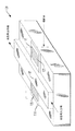
- 一端で入力光信号を受信し、他端で変調された光信号を出力するように構成された半導体平面光導波路コアと、
前記半導体平面光導波路コアの両側に隣接するように配置され、前記入力光信号が前記半導体平面光導波路コアを伝播する間、前記入力光信号の伝播方向に横切って前記半導体平面光導波路コアに電圧を印加することができる第1および第2のドープされた半導体接続パスと、
電圧源と、
を含む光変調器を備える装置であって、
前記半導体平面光導波路コアならびに前記第1および第2のドープされた半導体接続パスが、連続したPN半導体接合部を有する構造を形成し、
前記半導体平面光導波路コアが、前記連続した接合部の両方において接合面を形成し、
前記第1および第2のドープされた半導体接続パス、前記連続したPN半導体接合部ならびに前記電圧源が直列に接続されている装置。 - 前記連続したPN半導体接合部の少なくとも1つが、真性半導体層または絶縁層をさらに含む、請求項1に記載の装置。
- 前記電圧源が、直流バイアス電圧0の交流信号を出力するように構成されている、請求項1に記載の装置。
- 導波路の半導体平面光導波路コア中の端部に入力光信号を送り込む工程と、
前記入力光信号の伝播方向に横切って、前記半導体平面光導波路コアの幅または高さの両端間に印加される電圧源からの出力電圧を変調する工程であって、前記半導体平面光導波路コアの両側に隣接するように配置された第1および第2のドープされた半導体接続パスを介して前記出力電圧が印加されることで、前記半導体平面光導波路コアに沿って前記入力光信号が伝播している間、前記第1および第2のドープされた半導体接続パスならびに前記半導体平面光導波路コアによって形成された連続したPN半導体接合部付近のキャリア密度が変調される工程と、
前記導波路の半導体平面光導波路コアの対向する端部から変調された光信号を出力する工程と、
を含む前記入力光信号を変調する工程を備える、半導体平面光導波路の動作方法であって、
各PN半導体接合部の一部分が、前記半導体平面光導波路コア中に配置され、
前記半導体平面光導波路コアが、前記接合部の両方において接合面を形成し、
前記第1および第2のドープされた半導体接続パス、前記連続したPN半導体接合部ならびに前記電圧源が直列に接続されている方法。 - 前記変調された光学信号が、前記電圧源の出力電圧の変調周波数の2倍で変調される、請求項4に記載の方法。
- 前記連続したPN半導体接合部の少なくとも1つが、ドープされた半導体層の間に挟まれた真性半導体層または絶縁層をさらに含む、請求項4に記載の方法。
Applications Claiming Priority (3)
| Application Number | Priority Date | Filing Date | Title |
|---|---|---|---|
| US11/681,070 US7672553B2 (en) | 2007-03-01 | 2007-03-01 | High speed semiconductor optical modulator |
| US11/681,070 | 2007-03-01 | ||
| PCT/US2007/022945 WO2008105854A1 (en) | 2007-03-01 | 2007-10-30 | High speed semiconductor optical modulator |
Related Child Applications (1)
| Application Number | Title | Priority Date | Filing Date |
|---|---|---|---|
| JP2013141219A Division JP6073753B2 (ja) | 2007-03-01 | 2013-07-05 | 高速の半導体光変調器 |
Publications (3)
| Publication Number | Publication Date |
|---|---|
| JP2010520506A JP2010520506A (ja) | 2010-06-10 |
| JP2010520506A5 JP2010520506A5 (ja) | 2012-07-19 |
| JP5551446B2 true JP5551446B2 (ja) | 2014-07-16 |
Family
ID=39046860
Family Applications (2)
| Application Number | Title | Priority Date | Filing Date |
|---|---|---|---|
| JP2009551977A Expired - Fee Related JP5551446B2 (ja) | 2007-03-01 | 2007-10-30 | 高速の半導体光変調器 |
| JP2013141219A Expired - Fee Related JP6073753B2 (ja) | 2007-03-01 | 2013-07-05 | 高速の半導体光変調器 |
Family Applications After (1)
| Application Number | Title | Priority Date | Filing Date |
|---|---|---|---|
| JP2013141219A Expired - Fee Related JP6073753B2 (ja) | 2007-03-01 | 2013-07-05 | 高速の半導体光変調器 |
Country Status (6)
| Country | Link |
|---|---|
| US (1) | US7672553B2 (ja) |
| EP (1) | EP2132595B1 (ja) |
| JP (2) | JP5551446B2 (ja) |
| KR (1) | KR101158969B1 (ja) |
| CN (1) | CN101622570B (ja) |
| WO (1) | WO2008105854A1 (ja) |
Families Citing this family (32)
| Publication number | Priority date | Publication date | Assignee | Title |
|---|---|---|---|---|
| US8488917B2 (en) * | 2008-09-24 | 2013-07-16 | Cornell University | Electro-optic modulator |
| US8041158B2 (en) | 2008-11-13 | 2011-10-18 | Alcatel Lucent | Multithickness layered electronic-photonic devices |
| US8548281B2 (en) * | 2009-09-08 | 2013-10-01 | Electronics And Telecommunications Research Institute | Electro-optic modulating device |
| GB2477131A (en) * | 2010-01-22 | 2011-07-27 | Univ Surrey | Electro-optic device |
| US8842942B2 (en) * | 2010-02-08 | 2014-09-23 | Samsung Electronics Co., Ltd. | Optical modulator formed on bulk-silicon substrate |
| KR101683543B1 (ko) * | 2010-02-08 | 2016-12-07 | 삼성전자 주식회사 | 벌크 실리콘 기판을 사용하는 변조기 |
| GB2477935A (en) * | 2010-02-17 | 2011-08-24 | Univ Surrey | Electro-optic device with a waveguide rib |
| CN101907785B (zh) * | 2010-06-11 | 2015-09-16 | 上海华虹宏力半导体制造有限公司 | 一种光调制器pn结的制作方法 |
| US8358897B1 (en) * | 2010-12-10 | 2013-01-22 | Aurrion, Llc | High index bonding layer for hybrid photonic devices |
| US9110314B2 (en) * | 2010-12-29 | 2015-08-18 | Agency For Science, Technology And Research | Optical modulator and a method of forming the same |
| US8542954B2 (en) * | 2012-02-01 | 2013-09-24 | Kotura, Inc. | Optical component having reduced dependency on etch depth |
| US9329415B2 (en) | 2012-11-05 | 2016-05-03 | Agency For Science, Technology And Research | Method for forming an optical modulator |
| JP6020096B2 (ja) * | 2012-11-30 | 2016-11-02 | 富士通株式会社 | 光変調器及び光送信器 |
| US9625746B2 (en) | 2012-12-11 | 2017-04-18 | Acacia Communications, Inc. | Silicon depletion modulators with enhanced slab doping |
| US10025120B2 (en) * | 2012-12-13 | 2018-07-17 | Luxtera, Inc. | Method and system for a low parasitic silicon high-speed phase modulator having raised fingers perpendicular to the PN junction |
| JP2014174306A (ja) * | 2013-03-08 | 2014-09-22 | Nippon Telegr & Teleph Corp <Ntt> | 光導波路構造 |
| FR3005512A1 (fr) | 2013-05-07 | 2014-11-14 | St Microelectronics Sa | Dephaseur electro-optique a faible coefficient d'absorption |
| US9939666B2 (en) | 2013-06-06 | 2018-04-10 | Acacia Communications, Inc. | Silicon electro-optical modulator |
| CN104583856B (zh) * | 2013-08-23 | 2017-09-29 | 华为技术有限公司 | 一种光调制器和光信号发射装置 |
| FR3018390A1 (fr) | 2014-03-10 | 2015-09-11 | St Microelectronics Crolles 2 | Dispositif de protection dynamique contre les decharges electrostatiques adapte aux dispositifs electro-optiques |
| CN106461985B (zh) * | 2014-05-30 | 2021-06-01 | 华为技术有限公司 | 电光调制器 |
| US9929725B2 (en) * | 2015-01-09 | 2018-03-27 | Northwestern University | System and method for anti-ambipolar heterojunctions from solution-processed semiconductors |
| US10514503B2 (en) | 2016-03-04 | 2019-12-24 | The Governing Council Of The University Of Toronto | System and method for manufacturing a semiconductor junction |
| CN107293601B (zh) * | 2016-04-12 | 2021-10-22 | 朱江 | 一种肖特基半导体装置及其制备方法 |
| CN106873192A (zh) * | 2016-11-07 | 2017-06-20 | 北京交通大学 | 基于硅波导的电光超快空间调制器 |
| CN110431475B (zh) * | 2017-01-18 | 2023-09-19 | 新飞通光电公司 | 用于基于半导体的mzm调制器的相位匹配的光波传播和rf波传播的方法和装置 |
| JP6983590B2 (ja) * | 2017-09-08 | 2021-12-17 | 技術研究組合光電子融合基盤技術研究所 | 光変調器及びその製造方法 |
| JP6823619B2 (ja) * | 2018-04-19 | 2021-02-03 | 日本電信電話株式会社 | 光変調器 |
| CN109324428B (zh) * | 2018-11-07 | 2021-11-12 | 三明学院 | 硅基电光调制器的调制臂长度设置方法及设备 |
| US10962811B2 (en) * | 2018-12-06 | 2021-03-30 | Sifotonics Technologies Co., Ltd. | Monolithic electro-optical modulator with comb-shaped transmission line |
| US10895764B1 (en) * | 2019-10-24 | 2021-01-19 | Veo, Inc. | Dielectric electro-optic phase shifter |
| CN110955067B (zh) * | 2019-12-12 | 2022-09-02 | 武汉邮电科学研究院有限公司 | 一种水平分层的脊形光波导器件的有源区结构及制造方法 |
Family Cites Families (19)
| Publication number | Priority date | Publication date | Assignee | Title |
|---|---|---|---|---|
| JPS61148427A (ja) * | 1984-12-24 | 1986-07-07 | Hitachi Ltd | 導波形光変調器 |
| US5164797A (en) * | 1988-06-17 | 1992-11-17 | Xerox Corporation | Lateral heterojunction bipolar transistor (LHBT) and suitability thereof as a hetero transverse junction (HTJ) laser |
| US4997246A (en) * | 1989-12-21 | 1991-03-05 | International Business Machines Corporation | Silicon-based rib waveguide optical modulator |
| JPH05158085A (ja) * | 1991-12-05 | 1993-06-25 | Fujitsu Ltd | 光変調装置及びその製造方法 |
| JPH07211936A (ja) * | 1994-01-21 | 1995-08-11 | Sony Corp | 半導体装置 |
| GB2323450A (en) * | 1997-03-20 | 1998-09-23 | Secr Defence | Optical modulator |
| GB2348293A (en) * | 1999-03-25 | 2000-09-27 | Bookham Technology Ltd | Optical phase modulator |
| US6627785B1 (en) * | 2000-02-29 | 2003-09-30 | Virginia Commwealth University | Wound dressings with protease-lowering activity |
| JP2002164352A (ja) * | 2000-09-13 | 2002-06-07 | Toshiba Corp | バイポーラトランジスタ、半導体発光素子、及び半導体素子 |
| GB2367187B (en) * | 2000-09-21 | 2002-11-13 | Bookham Technology Plc | An isolation device |
| EP1204145B1 (en) * | 2000-10-23 | 2011-12-28 | Panasonic Corporation | Semiconductor element |
| AU2002356330A1 (en) * | 2001-12-27 | 2003-07-30 | Bookham Technology Plc | An in-line waveguide photo detector |
| US6845198B2 (en) * | 2003-03-25 | 2005-01-18 | Sioptical, Inc. | High-speed silicon-based electro-optic modulator |
| US7085443B1 (en) | 2003-08-15 | 2006-08-01 | Luxtera, Inc. | Doping profiles in PN diode optical modulators |
| US7116853B2 (en) * | 2003-08-15 | 2006-10-03 | Luxtera, Inc. | PN diode optical modulators fabricated in rib waveguides |
| US7298949B2 (en) * | 2004-02-12 | 2007-11-20 | Sioptical, Inc. | SOI-based photonic bandgap devices |
| US20060000822A1 (en) * | 2004-02-23 | 2006-01-05 | Kyocera Corporation | Ceramic heater, wafer heating device using thereof and method for manufacturing a semiconductor substrate |
| AU2005257982B8 (en) * | 2004-06-16 | 2011-03-10 | Jack Arbiser | Carbazole formulations for the treatment of psoriasis and angiogenesis |
| US7280712B2 (en) | 2005-08-04 | 2007-10-09 | Intel Corporation | Method and apparatus for phase shifiting an optical beam in an optical device |
-
2007
- 2007-03-01 US US11/681,070 patent/US7672553B2/en not_active Expired - Fee Related
- 2007-10-30 CN CN2007800519416A patent/CN101622570B/zh not_active Expired - Fee Related
- 2007-10-30 JP JP2009551977A patent/JP5551446B2/ja not_active Expired - Fee Related
- 2007-10-30 EP EP07839857.5A patent/EP2132595B1/en not_active Not-in-force
- 2007-10-30 KR KR1020097018204A patent/KR101158969B1/ko not_active IP Right Cessation
- 2007-10-30 WO PCT/US2007/022945 patent/WO2008105854A1/en active Application Filing
-
2013
- 2013-07-05 JP JP2013141219A patent/JP6073753B2/ja not_active Expired - Fee Related
Also Published As
| Publication number | Publication date |
|---|---|
| WO2008105854A1 (en) | 2008-09-04 |
| CN101622570A (zh) | 2010-01-06 |
| US7672553B2 (en) | 2010-03-02 |
| JP2010520506A (ja) | 2010-06-10 |
| KR20090116769A (ko) | 2009-11-11 |
| EP2132595A1 (en) | 2009-12-16 |
| US20080212913A1 (en) | 2008-09-04 |
| JP2013238876A (ja) | 2013-11-28 |
| KR101158969B1 (ko) | 2012-06-21 |
| JP6073753B2 (ja) | 2017-02-01 |
| CN101622570B (zh) | 2012-07-18 |
| EP2132595B1 (en) | 2016-02-17 |
Similar Documents
| Publication | Publication Date | Title |
|---|---|---|
| JP5551446B2 (ja) | 高速の半導体光変調器 | |
| US11886056B2 (en) | Electro-optical modulator using waveguides with overlapping ridges | |
| US10191350B2 (en) | Waveguide modulators structures | |
| US8488917B2 (en) | Electro-optic modulator | |
| KR101157374B1 (ko) | Pn 다이오드를 사용하는 고속 실리콘 광 변조를 위한 방법 및 장치 | |
| JP6622228B2 (ja) | 光変調器及びその製造方法 | |
| US20060215949A1 (en) | Electro-optic modulation | |
| US10678115B2 (en) | Waveguide modulator structures | |
| US8548281B2 (en) | Electro-optic modulating device | |
| JP2010520506A5 (ja) | ||
| US20080199123A1 (en) | Ultrafast ge/si resonator-based modulators for optical data communications in silicon photonics | |
| US20090310901A1 (en) | High speed optical modulator | |
| CN115145057A (zh) | 多掺杂平板硅光学调制器 | |
| CN116794860A (zh) | 具有增强的相位调谐的混合金属氧化物半导体电容器 | |
| CN113960816A (zh) | 硅光调制器及其形成方法 | |
| WO2023238403A1 (ja) | 光変調器 | |
| KR101453473B1 (ko) | 전기-광학 변조 소자 | |
| Li et al. | Highly efficient optical modulators in silicon for next-generation networks |
Legal Events
| Date | Code | Title | Description |
|---|---|---|---|
| A621 | Written request for application examination |
Free format text: JAPANESE INTERMEDIATE CODE: A621 Effective date: 20100521 |
|
| A521 | Written amendment |
Free format text: JAPANESE INTERMEDIATE CODE: A523 Effective date: 20100607 |
|
| A977 | Report on retrieval |
Free format text: JAPANESE INTERMEDIATE CODE: A971007 Effective date: 20111114 |
|
| A131 | Notification of reasons for refusal |
Free format text: JAPANESE INTERMEDIATE CODE: A131 Effective date: 20111121 |
|
| A601 | Written request for extension of time |
Free format text: JAPANESE INTERMEDIATE CODE: A601 Effective date: 20120221 |
|
| A602 | Written permission of extension of time |
Free format text: JAPANESE INTERMEDIATE CODE: A602 Effective date: 20120228 |
|
| A601 | Written request for extension of time |
Free format text: JAPANESE INTERMEDIATE CODE: A601 Effective date: 20120321 |
|
| A602 | Written permission of extension of time |
Free format text: JAPANESE INTERMEDIATE CODE: A602 Effective date: 20120328 |
|
| A521 | Written amendment |
Free format text: JAPANESE INTERMEDIATE CODE: A523 Effective date: 20120521 |
|
| A524 | Written submission of copy of amendment under section 19 (pct) |
Free format text: JAPANESE INTERMEDIATE CODE: A524 Effective date: 20120521 |
|
| RD04 | Notification of resignation of power of attorney |
Free format text: JAPANESE INTERMEDIATE CODE: A7424 Effective date: 20120710 |
|
| A02 | Decision of refusal |
Free format text: JAPANESE INTERMEDIATE CODE: A02 Effective date: 20130305 |
|
| A521 | Written amendment |
Free format text: JAPANESE INTERMEDIATE CODE: A523 Effective date: 20130705 |
|
| A911 | Transfer to examiner for re-examination before appeal (zenchi) |
Free format text: JAPANESE INTERMEDIATE CODE: A911 Effective date: 20130812 |
|
| A131 | Notification of reasons for refusal |
Free format text: JAPANESE INTERMEDIATE CODE: A131 Effective date: 20131024 |
|
| A601 | Written request for extension of time |
Free format text: JAPANESE INTERMEDIATE CODE: A601 Effective date: 20140124 |
|
| A602 | Written permission of extension of time |
Free format text: JAPANESE INTERMEDIATE CODE: A602 Effective date: 20140131 |
|
| A521 | Written amendment |
Free format text: JAPANESE INTERMEDIATE CODE: A523 Effective date: 20140227 |
|
| TRDD | Decision of grant or rejection written | ||
| A01 | Written decision to grant a patent or to grant a registration (utility model) |
Free format text: JAPANESE INTERMEDIATE CODE: A01 Effective date: 20140424 |
|
| A61 | First payment of annual fees (during grant procedure) |
Free format text: JAPANESE INTERMEDIATE CODE: A61 Effective date: 20140522 |
|
| R150 | Certificate of patent or registration of utility model |
Ref document number: 5551446 Country of ref document: JP Free format text: JAPANESE INTERMEDIATE CODE: R150 |
|
| R250 | Receipt of annual fees |
Free format text: JAPANESE INTERMEDIATE CODE: R250 |
|
| LAPS | Cancellation because of no payment of annual fees |