JP5547495B2 - 半導体構造をエッチングするための、パルス化反応ガスを補充するパルス化プラズマシステム - Google Patents
半導体構造をエッチングするための、パルス化反応ガスを補充するパルス化プラズマシステム Download PDFInfo
- Publication number
- JP5547495B2 JP5547495B2 JP2009550927A JP2009550927A JP5547495B2 JP 5547495 B2 JP5547495 B2 JP 5547495B2 JP 2009550927 A JP2009550927 A JP 2009550927A JP 2009550927 A JP2009550927 A JP 2009550927A JP 5547495 B2 JP5547495 B2 JP 5547495B2
- Authority
- JP
- Japan
- Prior art keywords
- plasma
- state
- pulsed
- etching
- sample
- Prior art date
- Legal status (The legal status is an assumption and is not a legal conclusion. Google has not performed a legal analysis and makes no representation as to the accuracy of the status listed.)
- Expired - Fee Related
Links
Images


Classifications
-
- H—ELECTRICITY
- H01—ELECTRIC ELEMENTS
- H01J—ELECTRIC DISCHARGE TUBES OR DISCHARGE LAMPS
- H01J37/00—Discharge tubes with provision for introducing objects or material to be exposed to the discharge, e.g. for the purpose of examination or processing thereof
- H01J37/32—Gas-filled discharge tubes
- H01J37/32431—Constructional details of the reactor
-
- H—ELECTRICITY
- H01—ELECTRIC ELEMENTS
- H01L—SEMICONDUCTOR DEVICES NOT COVERED BY CLASS H10
- H01L21/00—Processes or apparatus adapted for the manufacture or treatment of semiconductor or solid state devices or of parts thereof
- H01L21/02—Manufacture or treatment of semiconductor devices or of parts thereof
- H01L21/04—Manufacture or treatment of semiconductor devices or of parts thereof the devices having at least one potential-jump barrier or surface barrier, e.g. PN junction, depletion layer or carrier concentration layer
- H01L21/18—Manufacture or treatment of semiconductor devices or of parts thereof the devices having at least one potential-jump barrier or surface barrier, e.g. PN junction, depletion layer or carrier concentration layer the devices having semiconductor bodies comprising elements of Group IV of the Periodic System or AIIIBV compounds with or without impurities, e.g. doping materials
- H01L21/30—Treatment of semiconductor bodies using processes or apparatus not provided for in groups H01L21/20 - H01L21/26
- H01L21/302—Treatment of semiconductor bodies using processes or apparatus not provided for in groups H01L21/20 - H01L21/26 to change their surface-physical characteristics or shape, e.g. etching, polishing, cutting
- H01L21/306—Chemical or electrical treatment, e.g. electrolytic etching
- H01L21/3065—Plasma etching; Reactive-ion etching
-
- H—ELECTRICITY
- H01—ELECTRIC ELEMENTS
- H01L—SEMICONDUCTOR DEVICES NOT COVERED BY CLASS H10
- H01L21/00—Processes or apparatus adapted for the manufacture or treatment of semiconductor or solid state devices or of parts thereof
- H01L21/02—Manufacture or treatment of semiconductor devices or of parts thereof
- H01L21/04—Manufacture or treatment of semiconductor devices or of parts thereof the devices having at least one potential-jump barrier or surface barrier, e.g. PN junction, depletion layer or carrier concentration layer
- H01L21/18—Manufacture or treatment of semiconductor devices or of parts thereof the devices having at least one potential-jump barrier or surface barrier, e.g. PN junction, depletion layer or carrier concentration layer the devices having semiconductor bodies comprising elements of Group IV of the Periodic System or AIIIBV compounds with or without impurities, e.g. doping materials
- H01L21/30—Treatment of semiconductor bodies using processes or apparatus not provided for in groups H01L21/20 - H01L21/26
- H01L21/31—Treatment of semiconductor bodies using processes or apparatus not provided for in groups H01L21/20 - H01L21/26 to form insulating layers thereon, e.g. for masking or by using photolithographic techniques; After treatment of these layers; Selection of materials for these layers
- H01L21/3105—After-treatment
- H01L21/311—Etching the insulating layers by chemical or physical means
- H01L21/31105—Etching inorganic layers
- H01L21/31111—Etching inorganic layers by chemical means
- H01L21/31116—Etching inorganic layers by chemical means by dry-etching
-
- H—ELECTRICITY
- H01—ELECTRIC ELEMENTS
- H01L—SEMICONDUCTOR DEVICES NOT COVERED BY CLASS H10
- H01L21/00—Processes or apparatus adapted for the manufacture or treatment of semiconductor or solid state devices or of parts thereof
- H01L21/02—Manufacture or treatment of semiconductor devices or of parts thereof
- H01L21/04—Manufacture or treatment of semiconductor devices or of parts thereof the devices having at least one potential-jump barrier or surface barrier, e.g. PN junction, depletion layer or carrier concentration layer
- H01L21/18—Manufacture or treatment of semiconductor devices or of parts thereof the devices having at least one potential-jump barrier or surface barrier, e.g. PN junction, depletion layer or carrier concentration layer the devices having semiconductor bodies comprising elements of Group IV of the Periodic System or AIIIBV compounds with or without impurities, e.g. doping materials
- H01L21/30—Treatment of semiconductor bodies using processes or apparatus not provided for in groups H01L21/20 - H01L21/26
- H01L21/31—Treatment of semiconductor bodies using processes or apparatus not provided for in groups H01L21/20 - H01L21/26 to form insulating layers thereon, e.g. for masking or by using photolithographic techniques; After treatment of these layers; Selection of materials for these layers
- H01L21/3205—Deposition of non-insulating-, e.g. conductive- or resistive-, layers on insulating layers; After-treatment of these layers
- H01L21/321—After treatment
- H01L21/3213—Physical or chemical etching of the layers, e.g. to produce a patterned layer from a pre-deposited extensive layer
- H01L21/32133—Physical or chemical etching of the layers, e.g. to produce a patterned layer from a pre-deposited extensive layer by chemical means only
- H01L21/32135—Physical or chemical etching of the layers, e.g. to produce a patterned layer from a pre-deposited extensive layer by chemical means only by vapour etching only
- H01L21/32136—Physical or chemical etching of the layers, e.g. to produce a patterned layer from a pre-deposited extensive layer by chemical means only by vapour etching only using plasmas
- H01L21/32137—Physical or chemical etching of the layers, e.g. to produce a patterned layer from a pre-deposited extensive layer by chemical means only by vapour etching only using plasmas of silicon-containing layers
-
- H—ELECTRICITY
- H01—ELECTRIC ELEMENTS
- H01J—ELECTRIC DISCHARGE TUBES OR DISCHARGE LAMPS
- H01J2237/00—Discharge tubes exposing object to beam, e.g. for analysis treatment, etching, imaging
- H01J2237/32—Processing objects by plasma generation
- H01J2237/33—Processing objects by plasma generation characterised by the type of processing
- H01J2237/334—Etching
Landscapes
- Engineering & Computer Science (AREA)
- Physics & Mathematics (AREA)
- Condensed Matter Physics & Semiconductors (AREA)
- Chemical & Material Sciences (AREA)
- Plasma & Fusion (AREA)
- General Physics & Mathematics (AREA)
- Manufacturing & Machinery (AREA)
- Computer Hardware Design (AREA)
- Microelectronics & Electronic Packaging (AREA)
- Power Engineering (AREA)
- Chemical Kinetics & Catalysis (AREA)
- General Chemical & Material Sciences (AREA)
- Analytical Chemistry (AREA)
- Inorganic Chemistry (AREA)
- Drying Of Semiconductors (AREA)
Description
Claims (9)
- サンプルのエッチング方法であって、
パルス化プラズマ・プロセスを適用することによって前記サンプルの一部をエッチングする工程を含み、
前記パルス化プラズマ・プロセスは、複数のデューティサイクルから成り、各デューティサイクルはプラズマのオン状態とオフ状態の組合せであり、オン状態から成る各デューティサイクルの部分はデューティサイクルの65%から75%であり、
前記オン状態の持続時間が、前記サンプルに隣接した反応領域におけるマイクロ・ローディングを阻止するのに十分に短く、且つ前記オフ状態の持続時間が、前記サンプルに隣接した前記反応領域からのエッチング副産物のセットの除去を可能にするのに十分に長く、
前記プラズマは、1つあるいはそれ以上の反応ガスから発生し、
均一なプラズマを形成するために、当該1つあるいはそれ以上の反応ガスは、前記プラズマの前記オフ状態の間に補充され、前記プラズマの前記オン状態の間には、前記反応ガスのいずれも補充されない、方法。 - 前記オン状態の間に前記サンプルに負のバイアスを加え、前記オフ状態の間に前記サンプルにゼロバイアスを加える、請求項1に記載の方法。
- 前記プラズマの前記オフ状態の持続時間を、エッチング副産物の50%超が前記反応領域から除去されるまでの時間に一致するように選択する、請求項1に記載の方法。
- 不活性ガスを使用して、前記プラズマの前記オフ状態の間に前記エッチング副産物のセットのエッチングを強化する、請求項1に記載の方法。
- 前記サンプルの一部をエッチングする方法は、前記サンプルの第2部分のエッチングを含み、
当該第2部分をエッチングする前に、連続プラズマ・プロセスを適用して前記サンプルの第1部分をエッチングする工程と、
前記連続プラズマ・プロセスを終了する工程と、
を更に含む、請求項1に記載の方法。 - 第2連続プラズマ・プロセスを適用することによって前記サンプルの第3部分をエッチングする工程と、
前記第2連続プラズマ・プロセスを終了する工程と、
第2パルス化プラズマ・プロセスを適用することによって前記サンプルの第4部分をエッチングする工程であって、前記第2パルス化プラズマ・プロセスが第2の複数のデューティサイクルから成り、各デューティサイクルが第2プラズマの第2オン状態と第2オフ状態の組合せであり、前記第2プラズマが第2反応ガスから発生し、そして前記第2反応ガスが前記第2プラズマの前記オン状態の間でなく前記オフ状態の間に補充される工程と
をさらに含む、請求項5に記載の方法。 - サンプルのエッチングに用いられるシステムであって、
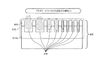
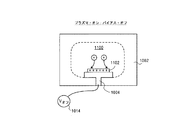
サンプル・ホルダーを備えたチャンバと、
前記チャンバに連結する排出デバイスであって、前記チャンバを減圧するための排出デバイスと、
前記チャンバに連結するガス注入デバイスであって、前記チャンバに1つあるいはそれ以上の反応ガスを注入するためのガス注入デバイスと、
前記チャンバに連結するプラズマ・イグニション・デバイスであって、前記1つあるいはそれ以上の反応ガスから誘導されるプラズマに点火するためのプラズマ・イグニション・デバイスと、
前記プラズマ・イグニション・デバイス及び前記ガス注入デバイスに連結するコンピューティング・デバイスであって、プロセッサ及びメモリを備え、この場合、前記メモリは、パルス化プラズマ・プロセスにおいて、前記プラズマ・イグニション・デバイスを制御することによりプラズマのオン状態とオフ状態の間を切り換えるための命令セットを含み、前記パルス化プラズマ・プロセスは複数のデューティサイクルから成り、各デューティサイクルは前記プラズマの1つのオン状態と1つのオフ状態の組合せであり、オン状態から成る各デューティサイクルの部分はデューティサイクルの65%から75%であり、
前記オン状態の持続時間が、サンプルに隣接する反応領域においてマイクロ・ローディングを抑止するのに十分に短く、且つ前記オフ状態の持続時間が、前記サンプルに隣接する前記反応領域からのエッチング副産物のセットの除去を可能にするのに十分に長く、
前記メモリは前記ガス注入デバイスを制御することにより開状態と閉状態の間を切換えるための命令セットも含み、前記プラズマは前記1つあるいはそれ以上の反応ガスから発生し、前記ガス注入デバイスが前記開状態であるときに前記1つあるいはそれ以上の反応ガスが補充され、そして
均一なプラズマを形成するために、前記プラズマの前記オフ状態の間に、前記1つあるいはそれ以上の反応ガスが補充され、前記プラズマの前記オン状態の間には、前記反応ガスのいずれも補充されない、コンピューティング・デバイスとを備えるシステム。 - 前記サンプル・ホルダーに連結する電圧源をさらに備え、前記電圧源が前記サンプルにバイアスを掛ける、請求項7に記載のシステム。
- 前記チャンバに連結する検出デバイスをさらに備え、前記検出デバイスが処理工程のエンドポイントを検出する、請求項7に記載のシステム。
Applications Claiming Priority (5)
| Application Number | Priority Date | Filing Date | Title |
|---|---|---|---|
| US11/677,472 | 2007-02-21 | ||
| US11/677,472 US7718538B2 (en) | 2007-02-21 | 2007-02-21 | Pulsed-plasma system with pulsed sample bias for etching semiconductor substrates |
| US11/678,047 | 2007-02-22 | ||
| US11/678,047 US7771606B2 (en) | 2007-02-22 | 2007-02-22 | Pulsed-plasma system with pulsed reaction gas replenish for etching semiconductors structures |
| PCT/US2008/002367 WO2008103453A1 (en) | 2007-02-21 | 2008-02-21 | Pulsed plasma system with pulsed reaction gas replenish for etching semiconductor structures |
Publications (3)
| Publication Number | Publication Date |
|---|---|
| JP2010519767A JP2010519767A (ja) | 2010-06-03 |
| JP2010519767A5 JP2010519767A5 (ja) | 2011-04-07 |
| JP5547495B2 true JP5547495B2 (ja) | 2014-07-16 |
Family
ID=39710407
Family Applications (1)
| Application Number | Title | Priority Date | Filing Date |
|---|---|---|---|
| JP2009550927A Expired - Fee Related JP5547495B2 (ja) | 2007-02-21 | 2008-02-21 | 半導体構造をエッチングするための、パルス化反応ガスを補充するパルス化プラズマシステム |
Country Status (3)
| Country | Link |
|---|---|
| JP (1) | JP5547495B2 (ja) |
| KR (1) | KR101470292B1 (ja) |
| WO (1) | WO2008103453A1 (ja) |
Families Citing this family (4)
| Publication number | Priority date | Publication date | Assignee | Title |
|---|---|---|---|---|
| US8969210B2 (en) * | 2010-09-15 | 2015-03-03 | Tokyo Electron Limited | Plasma etching apparatus, plasma etching method, and semiconductor device manufacturing method |
| JP6114622B2 (ja) * | 2013-04-26 | 2017-04-12 | 東京エレクトロン株式会社 | エッチング方法 |
| EP3087586B1 (en) | 2013-12-23 | 2021-09-29 | Intel Corporation | Advanced etching techniques for straight, tall and uniform fins across multiple fin pitch structures |
| JP5921580B2 (ja) * | 2014-01-15 | 2016-05-24 | 株式会社日立ハイテクノロジーズ | プラズマ処理方法 |
Family Cites Families (10)
| Publication number | Priority date | Publication date | Assignee | Title |
|---|---|---|---|---|
| JPS618925A (ja) * | 1984-06-23 | 1986-01-16 | Mitsubishi Electric Corp | エツチング方法 |
| JPH04110757U (ja) * | 1991-03-11 | 1992-09-25 | 神港精機株式会社 | 断続プラズマ装置 |
| US5877407A (en) * | 1997-07-22 | 1999-03-02 | Lucent Technologies Inc. | Plasma etch end point detection process |
| US6566272B2 (en) * | 1999-07-23 | 2003-05-20 | Applied Materials Inc. | Method for providing pulsed plasma during a portion of a semiconductor wafer process |
| JP2001085393A (ja) * | 1999-09-10 | 2001-03-30 | Hitachi Ltd | 表面加工方法 |
| JP2001313284A (ja) * | 2000-02-21 | 2001-11-09 | Hitachi Ltd | プラズマ処理方法および装置 |
| US6818562B2 (en) * | 2002-04-19 | 2004-11-16 | Applied Materials Inc | Method and apparatus for tuning an RF matching network in a plasma enhanced semiconductor wafer processing system |
| US8404594B2 (en) * | 2005-05-27 | 2013-03-26 | Freescale Semiconductor, Inc. | Reverse ALD |
| JP2006339562A (ja) * | 2005-06-06 | 2006-12-14 | Renesas Technology Corp | プラズマ処理方法及びそれを用いた半導体装置の製造方法 |
| US7718538B2 (en) * | 2007-02-21 | 2010-05-18 | Applied Materials, Inc. | Pulsed-plasma system with pulsed sample bias for etching semiconductor substrates |
-
2008
- 2008-02-21 JP JP2009550927A patent/JP5547495B2/ja not_active Expired - Fee Related
- 2008-02-21 WO PCT/US2008/002367 patent/WO2008103453A1/en active Application Filing
- 2008-02-21 KR KR1020097019675A patent/KR101470292B1/ko active IP Right Grant
Also Published As
| Publication number | Publication date |
|---|---|
| KR20090125112A (ko) | 2009-12-03 |
| KR101470292B1 (ko) | 2014-12-08 |
| WO2008103453A1 (en) | 2008-08-28 |
| JP2010519767A (ja) | 2010-06-03 |
Similar Documents
| Publication | Publication Date | Title |
|---|---|---|
| JP5774071B2 (ja) | パルス化したサンプルバイアスを用いる、半導体構造をエッチングするためのパルス化プラズマシステム | |
| US7771606B2 (en) | Pulsed-plasma system with pulsed reaction gas replenish for etching semiconductors structures | |
| US7737042B2 (en) | Pulsed-plasma system for etching semiconductor structures | |
| Banna et al. | Pulsed high-density plasmas for advanced dry etching processes | |
| TWI483305B (zh) | 使用電漿脈衝來控制溝槽微負載的方法 | |
| CN101511969B (zh) | 用于干法刻蚀含铪材料的方法和系统 | |
| JP2010045171A (ja) | 半導体加工方法 | |
| US11158507B2 (en) | In-situ high power implant to relieve stress of a thin film | |
| US11398386B2 (en) | Plasma etch processes | |
| JP5547495B2 (ja) | 半導体構造をエッチングするための、パルス化反応ガスを補充するパルス化プラズマシステム | |
| CN114175215A (zh) | 用于干式蚀刻化合物材料的方法 | |
| JP2022027715A (ja) | 金属酸化物のプラズマ支援エッチング | |
| US20170062225A1 (en) | Method for Etching a Silicon-Containing Substrate | |
| US20110171833A1 (en) | Dry etching method of high-k film | |
| US11527414B2 (en) | Methods for etching structures with oxygen pulsing | |
| KR101133697B1 (ko) | 반도체소자 가공방법 | |
| WO2008103454A2 (en) | Pulsed plasma system for etching semiconductor structures | |
| KR19980033895A (ko) | 독립적으로 제어되는 3전극을 가진 에칭 챔버 |
Legal Events
| Date | Code | Title | Description |
|---|---|---|---|
| A521 | Written amendment |
Free format text: JAPANESE INTERMEDIATE CODE: A523 Effective date: 20110218 |
|
| A621 | Written request for application examination |
Free format text: JAPANESE INTERMEDIATE CODE: A621 Effective date: 20110218 |
|
| A977 | Report on retrieval |
Free format text: JAPANESE INTERMEDIATE CODE: A971007 Effective date: 20120411 |
|
| A131 | Notification of reasons for refusal |
Free format text: JAPANESE INTERMEDIATE CODE: A131 Effective date: 20120418 |
|
| A601 | Written request for extension of time |
Free format text: JAPANESE INTERMEDIATE CODE: A601 Effective date: 20120717 |
|
| A602 | Written permission of extension of time |
Free format text: JAPANESE INTERMEDIATE CODE: A602 Effective date: 20120724 |
|
| A601 | Written request for extension of time |
Free format text: JAPANESE INTERMEDIATE CODE: A601 Effective date: 20120815 |
|
| A602 | Written permission of extension of time |
Free format text: JAPANESE INTERMEDIATE CODE: A602 Effective date: 20120827 |
|
| A521 | Written amendment |
Free format text: JAPANESE INTERMEDIATE CODE: A523 Effective date: 20120913 |
|
| A02 | Decision of refusal |
Free format text: JAPANESE INTERMEDIATE CODE: A02 Effective date: 20121120 |
|
| A521 | Written amendment |
Free format text: JAPANESE INTERMEDIATE CODE: A523 Effective date: 20130318 |
|
| A911 | Transfer to examiner for re-examination before appeal (zenchi) |
Free format text: JAPANESE INTERMEDIATE CODE: A911 Effective date: 20130326 |
|
| A912 | Re-examination (zenchi) completed and case transferred to appeal board |
Free format text: JAPANESE INTERMEDIATE CODE: A912 Effective date: 20130419 |
|
| A521 | Written amendment |
Free format text: JAPANESE INTERMEDIATE CODE: A523 Effective date: 20140326 |
|
| A61 | First payment of annual fees (during grant procedure) |
Free format text: JAPANESE INTERMEDIATE CODE: A61 Effective date: 20140515 |
|
| R150 | Certificate of patent or registration of utility model |
Ref document number: 5547495 Country of ref document: JP Free format text: JAPANESE INTERMEDIATE CODE: R150 |
|
| LAPS | Cancellation because of no payment of annual fees |