JP5491077B2 - 半導体装置、及び半導体装置の製造方法 - Google Patents
半導体装置、及び半導体装置の製造方法 Download PDFInfo
- Publication number
- JP5491077B2 JP5491077B2 JP2009137721A JP2009137721A JP5491077B2 JP 5491077 B2 JP5491077 B2 JP 5491077B2 JP 2009137721 A JP2009137721 A JP 2009137721A JP 2009137721 A JP2009137721 A JP 2009137721A JP 5491077 B2 JP5491077 B2 JP 5491077B2
- Authority
- JP
- Japan
- Prior art keywords
- insulating film
- conductive line
- insulator
- semiconductor device
- width
- Prior art date
- Legal status (The legal status is an assumption and is not a legal conclusion. Google has not performed a legal analysis and makes no representation as to the accuracy of the status listed.)
- Expired - Fee Related
Links
- 239000004065 semiconductor Substances 0.000 title claims description 79
- 238000004519 manufacturing process Methods 0.000 title claims description 28
- 238000000034 method Methods 0.000 claims description 72
- 239000012212 insulator Substances 0.000 claims description 53
- 238000006243 chemical reaction Methods 0.000 claims description 43
- 238000005530 etching Methods 0.000 claims description 43
- 239000000758 substrate Substances 0.000 claims description 29
- 239000004020 conductor Substances 0.000 claims description 4
- 239000010410 layer Substances 0.000 description 63
- 230000008569 process Effects 0.000 description 46
- 238000009792 diffusion process Methods 0.000 description 29
- 238000005498 polishing Methods 0.000 description 24
- 238000003384 imaging method Methods 0.000 description 22
- 230000001629 suppression Effects 0.000 description 19
- 238000001312 dry etching Methods 0.000 description 17
- 229910052751 metal Inorganic materials 0.000 description 17
- 239000002184 metal Substances 0.000 description 17
- 229910004298 SiO 2 Inorganic materials 0.000 description 14
- 238000005268 plasma chemical vapour deposition Methods 0.000 description 12
- 238000000206 photolithography Methods 0.000 description 9
- 229910000765 intermetallic Inorganic materials 0.000 description 8
- RYGMFSIKBFXOCR-UHFFFAOYSA-N Copper Chemical group [Cu] RYGMFSIKBFXOCR-UHFFFAOYSA-N 0.000 description 7
- 229910052802 copper Inorganic materials 0.000 description 7
- 239000010949 copper Substances 0.000 description 7
- 230000009977 dual effect Effects 0.000 description 7
- ATJFFYVFTNAWJD-UHFFFAOYSA-N Tin Chemical compound [Sn] ATJFFYVFTNAWJD-UHFFFAOYSA-N 0.000 description 6
- 239000000463 material Substances 0.000 description 6
- 230000003287 optical effect Effects 0.000 description 5
- 230000006870 function Effects 0.000 description 4
- 238000002955 isolation Methods 0.000 description 4
- 238000004544 sputter deposition Methods 0.000 description 4
- WFKWXMTUELFFGS-UHFFFAOYSA-N tungsten Chemical compound [W] WFKWXMTUELFFGS-UHFFFAOYSA-N 0.000 description 4
- 229910052721 tungsten Inorganic materials 0.000 description 4
- 239000010937 tungsten Substances 0.000 description 4
- 229910016570 AlCu Inorganic materials 0.000 description 3
- 229910045601 alloy Inorganic materials 0.000 description 3
- 239000000956 alloy Substances 0.000 description 3
- 238000010586 diagram Methods 0.000 description 3
- 239000011229 interlayer Substances 0.000 description 3
- 238000000059 patterning Methods 0.000 description 3
- 229910052782 aluminium Inorganic materials 0.000 description 2
- XAGFODPZIPBFFR-UHFFFAOYSA-N aluminium Chemical compound [Al] XAGFODPZIPBFFR-UHFFFAOYSA-N 0.000 description 2
- 230000004888 barrier function Effects 0.000 description 2
- 239000011521 glass Substances 0.000 description 2
- 230000003071 parasitic effect Effects 0.000 description 2
- 229910021420 polycrystalline silicon Inorganic materials 0.000 description 2
- 229920005591 polysilicon Polymers 0.000 description 2
- 230000008901 benefit Effects 0.000 description 1
- 230000015572 biosynthetic process Effects 0.000 description 1
- 238000009413 insulation Methods 0.000 description 1
- 238000005468 ion implantation Methods 0.000 description 1
- 229920002120 photoresistant polymer Polymers 0.000 description 1
- 238000007747 plating Methods 0.000 description 1
- 238000007517 polishing process Methods 0.000 description 1
- 230000009467 reduction Effects 0.000 description 1
- 239000011347 resin Substances 0.000 description 1
- 229920005989 resin Polymers 0.000 description 1
- 230000004044 response Effects 0.000 description 1
- 238000009751 slip forming Methods 0.000 description 1
- 239000000126 substance Substances 0.000 description 1
Images


Classifications
-
- H—ELECTRICITY
- H01—ELECTRIC ELEMENTS
- H01L—SEMICONDUCTOR DEVICES NOT COVERED BY CLASS H10
- H01L31/00—Semiconductor devices sensitive to infrared radiation, light, electromagnetic radiation of shorter wavelength or corpuscular radiation and specially adapted either for the conversion of the energy of such radiation into electrical energy or for the control of electrical energy by such radiation; Processes or apparatus specially adapted for the manufacture or treatment thereof or of parts thereof; Details thereof
- H01L31/18—Processes or apparatus specially adapted for the manufacture or treatment of these devices or of parts thereof
-
- H—ELECTRICITY
- H01—ELECTRIC ELEMENTS
- H01L—SEMICONDUCTOR DEVICES NOT COVERED BY CLASS H10
- H01L21/00—Processes or apparatus adapted for the manufacture or treatment of semiconductor or solid state devices or of parts thereof
- H01L21/70—Manufacture or treatment of devices consisting of a plurality of solid state components formed in or on a common substrate or of parts thereof; Manufacture of integrated circuit devices or of parts thereof
- H01L21/71—Manufacture of specific parts of devices defined in group H01L21/70
- H01L21/768—Applying interconnections to be used for carrying current between separate components within a device comprising conductors and dielectrics
- H01L21/76801—Applying interconnections to be used for carrying current between separate components within a device comprising conductors and dielectrics characterised by the formation and the after-treatment of the dielectrics, e.g. smoothing
- H01L21/7682—Applying interconnections to be used for carrying current between separate components within a device comprising conductors and dielectrics characterised by the formation and the after-treatment of the dielectrics, e.g. smoothing the dielectric comprising air gaps
-
- H—ELECTRICITY
- H01—ELECTRIC ELEMENTS
- H01L—SEMICONDUCTOR DEVICES NOT COVERED BY CLASS H10
- H01L23/00—Details of semiconductor or other solid state devices
- H01L23/52—Arrangements for conducting electric current within the device in operation from one component to another, i.e. interconnections, e.g. wires, lead frames
- H01L23/522—Arrangements for conducting electric current within the device in operation from one component to another, i.e. interconnections, e.g. wires, lead frames including external interconnections consisting of a multilayer structure of conductive and insulating layers inseparably formed on the semiconductor body
- H01L23/5222—Capacitive arrangements or effects of, or between wiring layers
-
- H—ELECTRICITY
- H01—ELECTRIC ELEMENTS
- H01L—SEMICONDUCTOR DEVICES NOT COVERED BY CLASS H10
- H01L23/00—Details of semiconductor or other solid state devices
- H01L23/52—Arrangements for conducting electric current within the device in operation from one component to another, i.e. interconnections, e.g. wires, lead frames
- H01L23/522—Arrangements for conducting electric current within the device in operation from one component to another, i.e. interconnections, e.g. wires, lead frames including external interconnections consisting of a multilayer structure of conductive and insulating layers inseparably formed on the semiconductor body
- H01L23/532—Arrangements for conducting electric current within the device in operation from one component to another, i.e. interconnections, e.g. wires, lead frames including external interconnections consisting of a multilayer structure of conductive and insulating layers inseparably formed on the semiconductor body characterised by the materials
- H01L23/5329—Insulating materials
- H01L23/53295—Stacked insulating layers
-
- H—ELECTRICITY
- H01—ELECTRIC ELEMENTS
- H01L—SEMICONDUCTOR DEVICES NOT COVERED BY CLASS H10
- H01L27/00—Devices consisting of a plurality of semiconductor or other solid-state components formed in or on a common substrate
- H01L27/14—Devices consisting of a plurality of semiconductor or other solid-state components formed in or on a common substrate including semiconductor components sensitive to infrared radiation, light, electromagnetic radiation of shorter wavelength or corpuscular radiation and specially adapted either for the conversion of the energy of such radiation into electrical energy or for the control of electrical energy by such radiation
- H01L27/144—Devices controlled by radiation
- H01L27/146—Imager structures
- H01L27/14601—Structural or functional details thereof
- H01L27/14632—Wafer-level processed structures
-
- H—ELECTRICITY
- H01—ELECTRIC ELEMENTS
- H01L—SEMICONDUCTOR DEVICES NOT COVERED BY CLASS H10
- H01L27/00—Devices consisting of a plurality of semiconductor or other solid-state components formed in or on a common substrate
- H01L27/14—Devices consisting of a plurality of semiconductor or other solid-state components formed in or on a common substrate including semiconductor components sensitive to infrared radiation, light, electromagnetic radiation of shorter wavelength or corpuscular radiation and specially adapted either for the conversion of the energy of such radiation into electrical energy or for the control of electrical energy by such radiation
- H01L27/144—Devices controlled by radiation
- H01L27/146—Imager structures
- H01L27/14601—Structural or functional details thereof
- H01L27/14636—Interconnect structures
-
- H—ELECTRICITY
- H01—ELECTRIC ELEMENTS
- H01L—SEMICONDUCTOR DEVICES NOT COVERED BY CLASS H10
- H01L2924/00—Indexing scheme for arrangements or methods for connecting or disconnecting semiconductor or solid-state bodies as covered by H01L24/00
- H01L2924/0001—Technical content checked by a classifier
- H01L2924/0002—Not covered by any one of groups H01L24/00, H01L24/00 and H01L2224/00
-
- H—ELECTRICITY
- H01—ELECTRIC ELEMENTS
- H01L—SEMICONDUCTOR DEVICES NOT COVERED BY CLASS H10
- H01L2924/00—Indexing scheme for arrangements or methods for connecting or disconnecting semiconductor or solid-state bodies as covered by H01L24/00
- H01L2924/10—Details of semiconductor or other solid state devices to be connected
- H01L2924/11—Device type
- H01L2924/12—Passive devices, e.g. 2 terminal devices
- H01L2924/1204—Optical Diode
- H01L2924/12044—OLED
Description
Claims (6)
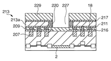
- 光電変換部を含む半導体基板と、
前記半導体基板の上に配された多層配線構造と、
を備え、
前記多層配線構造は、
複数の第1の導電ラインと、
前記複数の第1の導電ラインを覆う絶縁膜と、
前記複数の第1の導電ラインと交差するように前記絶縁膜の上に配された第2の導電ラインと、
を含み、
前記絶縁膜は、前記複数の第1の導電ラインと前記第2の導電ラインとが交差する複数の領域における少なくとも一部の領域にギャップを有し、前記光電変換部の上にギャップを有さず、
前記第2の導電ラインに沿った方向における前記ギャップの幅は、前記第1の導電ラインの幅以下である
ことを特徴とする半導体装置。 - 前記第1の導電ラインに沿った方向における前記ギャップの幅は、前記第2の導電ラインの幅以下である
ことを特徴とする請求項1に記載の半導体装置。 - 半導体基板を有する半導体装置の製造方法であって、
前記半導体基板の上方に複数の第1の導電ラインを形成する第1の工程と、
前記複数の第1の導電ラインを覆うように絶縁膜を形成する第2の工程と、
前記絶縁膜に前記複数の第1の導電ラインの上面の一部を露出する複数の溝をそれぞれ前記第1の導電ラインの幅以下の幅で形成する第3の工程と、
前記複数の溝のそれぞれに第1の絶縁体を埋め込む第4の工程と、
前記絶縁膜及び前記第1の絶縁体の上に、前記複数の第1の導電ラインと交差するように第2の導電ラインを形成する第5の工程と、
前記第5の工程の後に、前記第1の絶縁体を前記複数の溝のそれぞれから除去する第6の工程と、
前記第6の工程の後に、前記複数の溝内の前記第1の導電ラインと前記第2の導電ラインとが交差する複数の領域における少なくとも一部の領域をギャップとして残すように、前記複数の溝のそれぞれにおける前記半導体基板の表面に垂直な方向から見た場合に前記第2の導電ラインが重ならない部分に第2の絶縁体を埋め込む第7の工程と、
を含み、
前記第2の導電ラインに沿った方向における前記ギャップの幅は、前記第1の導電ラインの幅以下である
ことを特徴とする半導体装置の製造方法。 - 前記第6の工程では、前記第1の絶縁体の上面のうち前記半導体基板の表面に垂直な方向から見た場合に前記第2の導電ラインが重ならない部分が露出した状態で、前記第1の絶縁体の前記絶縁膜及び前記第2の導電ラインに対するエッチング選択比が高くなる条件で等方性エッチングを行うことにより、前記第1の絶縁体を前記複数の溝のそれぞれから除去する
ことを特徴とする請求項3に記載の半導体装置の製造方法。 - 前記第5の工程は、
前記絶縁膜及び前記第1の絶縁体の上に第2の絶縁膜を形成する工程と、
前記第2の絶縁膜に、前記複数の第1の導電ラインと交差するように第2の溝を形成する工程と、
前記第2の溝に導電体を埋め込むことにより、前記第2の溝に対応した前記第2の導電ラインを形成する工程と、
を含み、
前記第6の工程は、
前記第1の絶縁体の上面のうち前記半導体基板の表面に垂直な方向から見た場合に前記第2の導電ラインが重ならない部分を露出するように複数の穴を前記第2の絶縁膜に形成する工程と、
前記絶縁膜及び前記第2の導電ラインに対する前記第1の絶縁体のエッチング選択比が高くなる条件で前記複数の穴を介して等方性エッチングを行うことにより、前記第1の絶縁体を前記複数の溝のそれぞれから除去する工程と、
を含み、
前記第7の工程では、
前記複数の穴を介して前記複数の溝のそれぞれに前記第2の絶縁体を埋め込む
ことを特徴とする請求項3に記載の半導体装置の製造方法。 - 前記半導体装置は、光電変換装置を含み、
前記半導体基板は、光電変換部を含む
ことを特徴とする請求項3から5のいずれか1項に記載の半導体装置の製造方法。
Priority Applications (5)
| Application Number | Priority Date | Filing Date | Title |
|---|---|---|---|
| JP2009137721A JP5491077B2 (ja) | 2009-06-08 | 2009-06-08 | 半導体装置、及び半導体装置の製造方法 |
| EP10161984.9A EP2261968B1 (en) | 2009-06-08 | 2010-05-05 | Method of manufacturing a semiconductor device |
| US12/782,889 US8350300B2 (en) | 2009-06-08 | 2010-05-19 | Semiconductor device having air gaps in multilayer wiring structure |
| CN201010196500.9A CN101908525B (zh) | 2009-06-08 | 2010-06-03 | 半导体器件以及制造所述半导体器件的方法 |
| US13/707,887 US8748210B2 (en) | 2009-06-08 | 2012-12-07 | Method of manufacturing semiconductor device having air gaps in multilayer wiring structure |
Applications Claiming Priority (1)
| Application Number | Priority Date | Filing Date | Title |
|---|---|---|---|
| JP2009137721A JP5491077B2 (ja) | 2009-06-08 | 2009-06-08 | 半導体装置、及び半導体装置の製造方法 |
Publications (3)
| Publication Number | Publication Date |
|---|---|
| JP2010283307A JP2010283307A (ja) | 2010-12-16 |
| JP2010283307A5 JP2010283307A5 (ja) | 2012-07-26 |
| JP5491077B2 true JP5491077B2 (ja) | 2014-05-14 |
Family
ID=42712730
Family Applications (1)
| Application Number | Title | Priority Date | Filing Date |
|---|---|---|---|
| JP2009137721A Expired - Fee Related JP5491077B2 (ja) | 2009-06-08 | 2009-06-08 | 半導体装置、及び半導体装置の製造方法 |
Country Status (4)
| Country | Link |
|---|---|
| US (2) | US8350300B2 (ja) |
| EP (1) | EP2261968B1 (ja) |
| JP (1) | JP5491077B2 (ja) |
| CN (1) | CN101908525B (ja) |
Families Citing this family (8)
| Publication number | Priority date | Publication date | Assignee | Title |
|---|---|---|---|---|
| JP5422455B2 (ja) * | 2010-03-23 | 2014-02-19 | パナソニック株式会社 | 固体撮像装置 |
| JP6184061B2 (ja) | 2012-05-29 | 2017-08-23 | キヤノン株式会社 | 積層型半導体装置及び電子機器 |
| US8921901B1 (en) * | 2013-06-10 | 2014-12-30 | United Microelectronics Corp. | Stacked CMOS image sensor and signal processor wafer structure |
| JP6856974B2 (ja) * | 2015-03-31 | 2021-04-14 | ソニーセミコンダクタソリューションズ株式会社 | 固体撮像素子および電子機器 |
| CN114744002A (zh) * | 2015-03-31 | 2022-07-12 | 索尼半导体解决方案公司 | 半导体装置 |
| US10211146B2 (en) | 2016-05-12 | 2019-02-19 | Globalfoundries Inc. | Air gap over transistor gate and related method |
| US10157777B2 (en) * | 2016-05-12 | 2018-12-18 | Globalfoundries Inc. | Air gap over transistor gate and related method |
| EP3506342A4 (en) * | 2016-08-25 | 2019-08-28 | Sony Semiconductor Solutions Corporation | SEMICONDUCTOR COMPONENT, IMAGE RECORDING DEVICE AND METHOD FOR PRODUCING A SEMICONDUCTOR CONSTRUCTION ELEMENT |
Family Cites Families (21)
| Publication number | Priority date | Publication date | Assignee | Title |
|---|---|---|---|---|
| NL181611C (nl) * | 1978-11-14 | 1987-09-16 | Philips Nv | Werkwijze ter vervaardiging van een bedradingssysteem, alsmede een halfgeleiderinrichting voorzien van een dergelijk bedradingssysteem. |
| JPH0536841A (ja) | 1991-08-01 | 1993-02-12 | Matsushita Electric Ind Co Ltd | 半導体装置及びその製造方法 |
| JP2836542B2 (ja) * | 1995-10-17 | 1998-12-14 | 日本電気株式会社 | 半導体装置の製造方法 |
| JP3129284B2 (ja) * | 1998-05-08 | 2001-01-29 | 日本電気株式会社 | 半導集積回路装置の製造方法 |
| US6211561B1 (en) * | 1998-11-16 | 2001-04-03 | Conexant Systems, Inc. | Interconnect structure and method employing air gaps between metal lines and between metal layers |
| JP2001015592A (ja) * | 1999-06-28 | 2001-01-19 | Sony Corp | 半導体装置 |
| US6423629B1 (en) * | 2000-05-31 | 2002-07-23 | Kie Y. Ahn | Multilevel copper interconnects with low-k dielectrics and air gaps |
| US6984577B1 (en) * | 2000-09-20 | 2006-01-10 | Newport Fab, Llc | Damascene interconnect structure and fabrication method having air gaps between metal lines and metal layers |
| JP3481222B2 (ja) * | 2001-09-07 | 2003-12-22 | 松下電器産業株式会社 | 配線構造及びその設計方法 |
| US6713835B1 (en) * | 2003-05-22 | 2004-03-30 | International Business Machines Corporation | Method for manufacturing a multi-level interconnect structure |
| JP2007523465A (ja) * | 2003-05-26 | 2007-08-16 | コーニンクレッカ フィリップス エレクトロニクス エヌ ヴィ | 多孔質の誘電体層とエアギャップとを有する基板の製造方法、および基板 |
| US7071532B2 (en) * | 2003-09-30 | 2006-07-04 | International Business Machines Corporation | Adjustable self-aligned air gap dielectric for low capacitance wiring |
| US7094689B2 (en) * | 2004-07-20 | 2006-08-22 | Taiwan Semiconductor Manufacturing Co., Ltd. | Air gap interconnect structure and method thereof |
| JP4717598B2 (ja) * | 2004-12-16 | 2011-07-06 | キヤノン株式会社 | レーザー回路基板 |
| US7214920B2 (en) * | 2005-05-06 | 2007-05-08 | Micron Technology, Inc. | Pixel with spatially varying metal route positions |
| WO2007020688A1 (ja) * | 2005-08-17 | 2007-02-22 | Fujitsu Limited | 半導体装置及びその製造方法 |
| JP2007184788A (ja) * | 2006-01-06 | 2007-07-19 | Nikon Corp | 固体撮像装置 |
| US7557424B2 (en) * | 2007-01-03 | 2009-07-07 | International Business Machines Corporation | Reversible electric fuse and antifuse structures for semiconductor devices |
| KR100843233B1 (ko) * | 2007-01-25 | 2008-07-03 | 삼성전자주식회사 | 배선층의 양측벽에 인접하여 에어갭을 갖는 반도체 소자 및그 제조방법 |
| KR100850273B1 (ko) * | 2007-03-08 | 2008-08-04 | 삼성전자주식회사 | 멀티 비트 전기 기계적 메모리 소자 및 그의 제조방법 |
| US7659595B2 (en) * | 2007-07-16 | 2010-02-09 | Taiwan Semiconductor Manufacturing Company, Ltd. | Embedded bonding pad for backside illuminated image sensor |
-
2009
- 2009-06-08 JP JP2009137721A patent/JP5491077B2/ja not_active Expired - Fee Related
-
2010
- 2010-05-05 EP EP10161984.9A patent/EP2261968B1/en not_active Not-in-force
- 2010-05-19 US US12/782,889 patent/US8350300B2/en not_active Expired - Fee Related
- 2010-06-03 CN CN201010196500.9A patent/CN101908525B/zh not_active Expired - Fee Related
-
2012
- 2012-12-07 US US13/707,887 patent/US8748210B2/en not_active Expired - Fee Related
Also Published As
| Publication number | Publication date |
|---|---|
| CN101908525B (zh) | 2014-12-24 |
| EP2261968B1 (en) | 2017-01-04 |
| US20130122644A1 (en) | 2013-05-16 |
| EP2261968A2 (en) | 2010-12-15 |
| US8748210B2 (en) | 2014-06-10 |
| US20100308430A1 (en) | 2010-12-09 |
| US8350300B2 (en) | 2013-01-08 |
| JP2010283307A (ja) | 2010-12-16 |
| CN101908525A (zh) | 2010-12-08 |
| EP2261968A3 (en) | 2012-09-12 |
Similar Documents
| Publication | Publication Date | Title |
|---|---|---|
| JP5491077B2 (ja) | 半導体装置、及び半導体装置の製造方法 | |
| JP4117672B2 (ja) | 固体撮像素子及び固体撮像装置、並びにこれらの製造方法 | |
| US10249665B2 (en) | Solid-state imaging device and method of manufacturing solid-state imaging device | |
| US10026769B2 (en) | Semiconductor device and solid-state imaging device | |
| JP5357441B2 (ja) | 固体撮像装置の製造方法 | |
| JP4384454B2 (ja) | イメージ素子 | |
| KR101107627B1 (ko) | 3차원 구조를 갖는 웨이퍼의 패드 형성 방법 | |
| JP4427949B2 (ja) | 固体撮像素子及びその製造方法 | |
| KR100666371B1 (ko) | 이미지 소자의 제조 방법 | |
| JP2011216865A (ja) | 固体撮像装置 | |
| JP2005209677A (ja) | 半導体装置 | |
| JP4866972B1 (ja) | 固体撮像装置及びその製造方法 | |
| JP2009016406A (ja) | 貫通導電体を有する半導体装置およびその製造方法 | |
| JP2013214616A (ja) | 固体撮像装置、固体撮像装置の製造方法及び電子機器 | |
| KR100524200B1 (ko) | 이미지 소자 및 그 제조 방법 | |
| KR100963141B1 (ko) | 광전 변환 장치 및 그 제조 방법 | |
| JP2009295733A (ja) | 半導体装置及びその製造方法 | |
| JP6192598B2 (ja) | 撮像装置およびその製造方法 | |
| JP6539123B2 (ja) | 固体撮像装置及びその製造方法ならびにカメラ | |
| CN101136424B (zh) | 图像传感器和其制造方法 | |
| JP2008199059A (ja) | 固体撮像素子及びその製造方法 | |
| JP5950531B2 (ja) | 半導体装置の製造方法及び半導体ウエハ | |
| JP5582879B2 (ja) | 半導体装置及びその製造方法 | |
| JP2015153870A (ja) | 半導体装置の製造方法、光電変換装置 | |
| KR100712817B1 (ko) | 반도체 장치 및 그 형성 방법 |
Legal Events
| Date | Code | Title | Description |
|---|---|---|---|
| A521 | Request for written amendment filed |
Free format text: JAPANESE INTERMEDIATE CODE: A523 Effective date: 20120607 |
|
| A621 | Written request for application examination |
Free format text: JAPANESE INTERMEDIATE CODE: A621 Effective date: 20120607 |
|
| A977 | Report on retrieval |
Free format text: JAPANESE INTERMEDIATE CODE: A971007 Effective date: 20130912 |
|
| A131 | Notification of reasons for refusal |
Free format text: JAPANESE INTERMEDIATE CODE: A131 Effective date: 20130920 |
|
| A521 | Request for written amendment filed |
Free format text: JAPANESE INTERMEDIATE CODE: A523 Effective date: 20131028 |
|
| TRDD | Decision of grant or rejection written | ||
| A01 | Written decision to grant a patent or to grant a registration (utility model) |
Free format text: JAPANESE INTERMEDIATE CODE: A01 Effective date: 20140131 |
|
| A61 | First payment of annual fees (during grant procedure) |
Free format text: JAPANESE INTERMEDIATE CODE: A61 Effective date: 20140227 |
|
| LAPS | Cancellation because of no payment of annual fees |