JP5450101B2 - 波長変換レーザ、画像表示装置、及びレーザ加工装置 - Google Patents
波長変換レーザ、画像表示装置、及びレーザ加工装置 Download PDFInfo
- Publication number
- JP5450101B2 JP5450101B2 JP2009550462A JP2009550462A JP5450101B2 JP 5450101 B2 JP5450101 B2 JP 5450101B2 JP 2009550462 A JP2009550462 A JP 2009550462A JP 2009550462 A JP2009550462 A JP 2009550462A JP 5450101 B2 JP5450101 B2 JP 5450101B2
- Authority
- JP
- Japan
- Prior art keywords
- fundamental wave
- wavelength conversion
- light
- wave
- converted
- Prior art date
- Legal status (The legal status is an assumption and is not a legal conclusion. Google has not performed a legal analysis and makes no representation as to the accuracy of the status listed.)
- Expired - Fee Related
Links
Images


Classifications
-
- G—PHYSICS
- G02—OPTICS
- G02F—OPTICAL DEVICES OR ARRANGEMENTS FOR THE CONTROL OF LIGHT BY MODIFICATION OF THE OPTICAL PROPERTIES OF THE MEDIA OF THE ELEMENTS INVOLVED THEREIN; NON-LINEAR OPTICS; FREQUENCY-CHANGING OF LIGHT; OPTICAL LOGIC ELEMENTS; OPTICAL ANALOGUE/DIGITAL CONVERTERS
- G02F1/00—Devices or arrangements for the control of the intensity, colour, phase, polarisation or direction of light arriving from an independent light source, e.g. switching, gating or modulating; Non-linear optics
- G02F1/35—Non-linear optics
- G02F1/37—Non-linear optics for second-harmonic generation
-
- H—ELECTRICITY
- H04—ELECTRIC COMMUNICATION TECHNIQUE
- H04N—PICTORIAL COMMUNICATION, e.g. TELEVISION
- H04N9/00—Details of colour television systems
- H04N9/12—Picture reproducers
- H04N9/31—Projection devices for colour picture display, e.g. using electronic spatial light modulators [ESLM]
- H04N9/3141—Constructional details thereof
- H04N9/315—Modulator illumination systems
- H04N9/3161—Modulator illumination systems using laser light sources
-
- G—PHYSICS
- G02—OPTICS
- G02B—OPTICAL ELEMENTS, SYSTEMS OR APPARATUS
- G02B6/00—Light guides; Structural details of arrangements comprising light guides and other optical elements, e.g. couplings
- G02B6/0001—Light guides; Structural details of arrangements comprising light guides and other optical elements, e.g. couplings specially adapted for lighting devices or systems
- G02B6/0011—Light guides; Structural details of arrangements comprising light guides and other optical elements, e.g. couplings specially adapted for lighting devices or systems the light guides being planar or of plate-like form
- G02B6/0013—Means for improving the coupling-in of light from the light source into the light guide
- G02B6/0023—Means for improving the coupling-in of light from the light source into the light guide provided by one optical element, or plurality thereof, placed between the light guide and the light source, or around the light source
- G02B6/0028—Light guide, e.g. taper
-
- G—PHYSICS
- G02—OPTICS
- G02B—OPTICAL ELEMENTS, SYSTEMS OR APPARATUS
- G02B6/00—Light guides; Structural details of arrangements comprising light guides and other optical elements, e.g. couplings
- G02B6/0001—Light guides; Structural details of arrangements comprising light guides and other optical elements, e.g. couplings specially adapted for lighting devices or systems
- G02B6/0011—Light guides; Structural details of arrangements comprising light guides and other optical elements, e.g. couplings specially adapted for lighting devices or systems the light guides being planar or of plate-like form
- G02B6/0075—Arrangements of multiple light guides
- G02B6/0078—Side-by-side arrangements, e.g. for large area displays
-
- G—PHYSICS
- G02—OPTICS
- G02F—OPTICAL DEVICES OR ARRANGEMENTS FOR THE CONTROL OF LIGHT BY MODIFICATION OF THE OPTICAL PROPERTIES OF THE MEDIA OF THE ELEMENTS INVOLVED THEREIN; NON-LINEAR OPTICS; FREQUENCY-CHANGING OF LIGHT; OPTICAL LOGIC ELEMENTS; OPTICAL ANALOGUE/DIGITAL CONVERTERS
- G02F1/00—Devices or arrangements for the control of the intensity, colour, phase, polarisation or direction of light arriving from an independent light source, e.g. switching, gating or modulating; Non-linear optics
- G02F1/01—Devices or arrangements for the control of the intensity, colour, phase, polarisation or direction of light arriving from an independent light source, e.g. switching, gating or modulating; Non-linear optics for the control of the intensity, phase, polarisation or colour
- G02F1/0147—Devices or arrangements for the control of the intensity, colour, phase, polarisation or direction of light arriving from an independent light source, e.g. switching, gating or modulating; Non-linear optics for the control of the intensity, phase, polarisation or colour based on thermo-optic effects
-
- G—PHYSICS
- G02—OPTICS
- G02F—OPTICAL DEVICES OR ARRANGEMENTS FOR THE CONTROL OF LIGHT BY MODIFICATION OF THE OPTICAL PROPERTIES OF THE MEDIA OF THE ELEMENTS INVOLVED THEREIN; NON-LINEAR OPTICS; FREQUENCY-CHANGING OF LIGHT; OPTICAL LOGIC ELEMENTS; OPTICAL ANALOGUE/DIGITAL CONVERTERS
- G02F1/00—Devices or arrangements for the control of the intensity, colour, phase, polarisation or direction of light arriving from an independent light source, e.g. switching, gating or modulating; Non-linear optics
- G02F1/29—Devices or arrangements for the control of the intensity, colour, phase, polarisation or direction of light arriving from an independent light source, e.g. switching, gating or modulating; Non-linear optics for the control of the position or the direction of light beams, i.e. deflection
-
- G—PHYSICS
- G02—OPTICS
- G02F—OPTICAL DEVICES OR ARRANGEMENTS FOR THE CONTROL OF LIGHT BY MODIFICATION OF THE OPTICAL PROPERTIES OF THE MEDIA OF THE ELEMENTS INVOLVED THEREIN; NON-LINEAR OPTICS; FREQUENCY-CHANGING OF LIGHT; OPTICAL LOGIC ELEMENTS; OPTICAL ANALOGUE/DIGITAL CONVERTERS
- G02F1/00—Devices or arrangements for the control of the intensity, colour, phase, polarisation or direction of light arriving from an independent light source, e.g. switching, gating or modulating; Non-linear optics
- G02F1/35—Non-linear optics
- G02F1/3501—Constructional details or arrangements of non-linear optical devices, e.g. shape of non-linear crystals
- G02F1/3503—Structural association of optical elements, e.g. lenses, with the non-linear optical device
-
- G—PHYSICS
- G02—OPTICS
- G02F—OPTICAL DEVICES OR ARRANGEMENTS FOR THE CONTROL OF LIGHT BY MODIFICATION OF THE OPTICAL PROPERTIES OF THE MEDIA OF THE ELEMENTS INVOLVED THEREIN; NON-LINEAR OPTICS; FREQUENCY-CHANGING OF LIGHT; OPTICAL LOGIC ELEMENTS; OPTICAL ANALOGUE/DIGITAL CONVERTERS
- G02F1/00—Devices or arrangements for the control of the intensity, colour, phase, polarisation or direction of light arriving from an independent light source, e.g. switching, gating or modulating; Non-linear optics
- G02F1/35—Non-linear optics
- G02F1/353—Frequency conversion, i.e. wherein a light beam is generated with frequency components different from those of the incident light beams
- G02F1/3544—Particular phase matching techniques
- G02F1/3546—Active phase matching, e.g. by electro- or thermo-optic tuning
-
- G—PHYSICS
- G02—OPTICS
- G02F—OPTICAL DEVICES OR ARRANGEMENTS FOR THE CONTROL OF LIGHT BY MODIFICATION OF THE OPTICAL PROPERTIES OF THE MEDIA OF THE ELEMENTS INVOLVED THEREIN; NON-LINEAR OPTICS; FREQUENCY-CHANGING OF LIGHT; OPTICAL LOGIC ELEMENTS; OPTICAL ANALOGUE/DIGITAL CONVERTERS
- G02F1/00—Devices or arrangements for the control of the intensity, colour, phase, polarisation or direction of light arriving from an independent light source, e.g. switching, gating or modulating; Non-linear optics
- G02F1/35—Non-linear optics
- G02F1/37—Non-linear optics for second-harmonic generation
- G02F1/372—Means for homogenizing the output beam
-
- G—PHYSICS
- G02—OPTICS
- G02F—OPTICAL DEVICES OR ARRANGEMENTS FOR THE CONTROL OF LIGHT BY MODIFICATION OF THE OPTICAL PROPERTIES OF THE MEDIA OF THE ELEMENTS INVOLVED THEREIN; NON-LINEAR OPTICS; FREQUENCY-CHANGING OF LIGHT; OPTICAL LOGIC ELEMENTS; OPTICAL ANALOGUE/DIGITAL CONVERTERS
- G02F2201/00—Constructional arrangements not provided for in groups G02F1/00 - G02F7/00
- G02F2201/17—Multi-pass arrangements, i.e. arrangements to pass light a plurality of times through the same element, e.g. by using an enhancement cavity
-
- G—PHYSICS
- G02—OPTICS
- G02F—OPTICAL DEVICES OR ARRANGEMENTS FOR THE CONTROL OF LIGHT BY MODIFICATION OF THE OPTICAL PROPERTIES OF THE MEDIA OF THE ELEMENTS INVOLVED THEREIN; NON-LINEAR OPTICS; FREQUENCY-CHANGING OF LIGHT; OPTICAL LOGIC ELEMENTS; OPTICAL ANALOGUE/DIGITAL CONVERTERS
- G02F2201/00—Constructional arrangements not provided for in groups G02F1/00 - G02F7/00
- G02F2201/34—Constructional arrangements not provided for in groups G02F1/00 - G02F7/00 reflector
-
- G—PHYSICS
- G02—OPTICS
- G02F—OPTICAL DEVICES OR ARRANGEMENTS FOR THE CONTROL OF LIGHT BY MODIFICATION OF THE OPTICAL PROPERTIES OF THE MEDIA OF THE ELEMENTS INVOLVED THEREIN; NON-LINEAR OPTICS; FREQUENCY-CHANGING OF LIGHT; OPTICAL LOGIC ELEMENTS; OPTICAL ANALOGUE/DIGITAL CONVERTERS
- G02F2203/00—Function characteristic
- G02F2203/05—Function characteristic wavelength dependent
-
- H—ELECTRICITY
- H01—ELECTRIC ELEMENTS
- H01S—DEVICES USING THE PROCESS OF LIGHT AMPLIFICATION BY STIMULATED EMISSION OF RADIATION [LASER] TO AMPLIFY OR GENERATE LIGHT; DEVICES USING STIMULATED EMISSION OF ELECTROMAGNETIC RADIATION IN WAVE RANGES OTHER THAN OPTICAL
- H01S5/00—Semiconductor lasers
- H01S5/005—Optical components external to the laser cavity, specially adapted therefor, e.g. for homogenisation or merging of the beams or for manipulating laser pulses, e.g. pulse shaping
- H01S5/0092—Optical components external to the laser cavity, specially adapted therefor, e.g. for homogenisation or merging of the beams or for manipulating laser pulses, e.g. pulse shaping for nonlinear frequency conversion, e.g. second harmonic generation [SHG] or sum- or difference-frequency generation outside the laser cavity
-
- H—ELECTRICITY
- H01—ELECTRIC ELEMENTS
- H01S—DEVICES USING THE PROCESS OF LIGHT AMPLIFICATION BY STIMULATED EMISSION OF RADIATION [LASER] TO AMPLIFY OR GENERATE LIGHT; DEVICES USING STIMULATED EMISSION OF ELECTROMAGNETIC RADIATION IN WAVE RANGES OTHER THAN OPTICAL
- H01S5/00—Semiconductor lasers
- H01S5/06—Arrangements for controlling the laser output parameters, e.g. by operating on the active medium
- H01S5/068—Stabilisation of laser output parameters
- H01S5/0683—Stabilisation of laser output parameters by monitoring the optical output parameters
- H01S5/0687—Stabilising the frequency of the laser
Landscapes
- Physics & Mathematics (AREA)
- Nonlinear Science (AREA)
- Optics & Photonics (AREA)
- Engineering & Computer Science (AREA)
- Multimedia (AREA)
- Signal Processing (AREA)
- General Physics & Mathematics (AREA)
- Optical Modulation, Optical Deflection, Nonlinear Optics, Optical Demodulation, Optical Logic Elements (AREA)
- Lasers (AREA)
Description
前記の式において、位相整合条件からのずれが生じると、変換効率が低下し、第2高調波(変換波)の発生が低下する。このため、位相整合条件からのずれが生じないように、非線形光学結晶の温度を許容範囲内の所定温度とする制御が行われている。
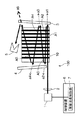
図1及び図2は、本発明の実施の形態1に係る波長変換レーザ100の概略構成図である。図1と図2とは、変換波光を優先して出射させる基本波光路を異ならせている点で相違している。
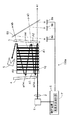
図5及び図6は、本発明の実施の形態2に係る波長変換レーザ200の概略構成図である。図5と図6とは、変換波光を優先して出射させる基本波光路を異ならせている点で相違している。
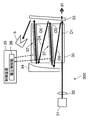
図7〜図9は本発明の実施の形態3に係る波長変換レーザ300の概略構成図である。図7と図9とは、変換波光を優先して出射させる基本波光路を異ならせている点で相違している。
Claims (10)
- 基本波を出射する基本波光源と、
前記基本波光源からの基本波を変換波光に変換するための波長変換素子と、
前記波長変換素子を異なる角度で通過する複数の基本波光路を規定するように前記基本波を反射する1対の基本波反射面と、
前記1対の基本波反射面の間で別々の方向を向く前記複数の基本波光路のうち、特定の基本波光路における波長変換効率が最も高くなるように波長変換効率を制御する制御装置とを備え、
前記1対の基本波反射面のうち少なくとも一方の反射面は、前記変換波光を透過する出力面であり、
前記制御装置は、前記波長変換素子の温度を制御する温度制御部を備え、
前記温度制御部は、前記波長変換素子を温度制御することにより前記特定の基本波光路を選択することを特徴とする波長変換レーザ。 - 基本波を出射する基本波光源と、
前記基本波光源からの基本波を変換波光に変換するための波長変換素子と、
前記波長変換素子を異なる角度で通過する複数の基本波光路を規定するように前記基本波を反射する1対の基本波反射面と、
前記1対の基本波反射面の間で別々の方向を向く前記複数の基本波光路のうち、特定の基本波光路における波長変換効率が最も高くなるように波長変換効率を制御する制御装置とを備え、
前記1対の基本波反射面のうち少なくとも一方の反射面は、前記変換波光を透過する出力面であり、
前記制御装置は、前記基本波光源による前記基本波の発振波長を制御する発振波長制御部を備え、
前記発振波長制御部は、前記基本波の発振波長を制御することにより前記特定の基本波光路を選択することを特徴とする波長変換レーザ。 - 基本波を出射する基本波光源と、
前記基本波光源からの基本波を変換波光に変換するための波長変換素子と、
前記波長変換素子を異なる角度で通過する複数の基本波光路を規定するように前記基本波を反射する1対の基本波反射面と、
前記1対の基本波反射面の間で別々の方向を向く前記複数の基本波光路のうち、特定の基本波光路における波長変換効率が最も高くなるように波長変換効率を制御する制御装置とを備え、
前記1対の基本波反射面のうち少なくとも一方の反射面は、前記変換波光を透過する出力面であり、
前記制御装置は、前記波長変換素子に電界を生じさせるために前記波長変換素子に電圧を印加する電圧制御部を備え、
前記電圧制御部は、前記波長変換素子に電界を生じさせることにより前記特定の基本波光路を選択することを特徴とする波長変換レーザ。 - 前記各基本波光路の少なくとも1つから出射された変換波光の光量を検出可能な受光素子をさらに備え、
前記制御装置は、前記受光素子により検出された光量に基づいて前記特定の基本波光路における波長変換効率が最も大きくなるように波長変換効率を制御することを特徴とする請求項1〜3の何れか1項に記載の波長変換レーザ。 - 前記制御装置は、前記各基本波光路のうち少なくとも2以上の光路において生じた変換波光を同時にマルチビームとして出射させるとともに、前記温度制御部が前記波長変換素子を温度制御することにより前記特定の基本波光路を選択することによって前記マルチビームの強度分布を制御することを特徴とする請求項1に記載の波長変換レーザ。
- 前記基本波光源は、前記基本波をパルス発振し、
前記制御装置は、前記各基本波光路のうち前記変換波光を出射させる光路の数を増減することにより、前記出力面から出射する変換波光のパルス幅、間隔の少なくとも一方を制御することを特徴とする請求項1〜5の何れか1項に記載の波長変換レーザ。 - 前記制御部は、前記各基本波光路のうち前記基本波が初めに通過する光路よりもその後に通過する光路における波長変換効率が大きくなるように波長変換効率を制御することを特徴とする請求項1〜6の何れか1項に記載の波長変換レーザ。
- 前記制御装置は、前記出力面から出射された変換波光が所定の範囲を走査するように、前記変換波光を出射する基本波光路を順次切り換えることを特徴とする請求項1〜7の何れか1項に記載の波長変換レーザ。
- 請求項1〜8の何れか1項に記載の波長変換レーザと、
所定の画像を表示するために前記波長変換レーザから出射された変換波光の変調を行う変調素子とを備えていることを特徴とする画像表示装置。 - 請求項1〜8の何れか1項に記載の波長変換レーザと、
前記波長変換レーザから出射された変換波光を集光する集光光学系とを備え、
前記各基本波光路のうち変換波光を出射させる光路の数を増減することにより、前記変換波光のスポット形状が変化することを特徴とするレーザ加工装置。
Priority Applications (1)
| Application Number | Priority Date | Filing Date | Title |
|---|---|---|---|
| JP2009550462A JP5450101B2 (ja) | 2008-01-21 | 2009-01-20 | 波長変換レーザ、画像表示装置、及びレーザ加工装置 |
Applications Claiming Priority (4)
| Application Number | Priority Date | Filing Date | Title |
|---|---|---|---|
| JP2008010876 | 2008-01-21 | ||
| JP2008010876 | 2008-01-21 | ||
| JP2009550462A JP5450101B2 (ja) | 2008-01-21 | 2009-01-20 | 波長変換レーザ、画像表示装置、及びレーザ加工装置 |
| PCT/JP2009/000176 WO2009093439A1 (ja) | 2008-01-21 | 2009-01-20 | 波長変換レーザ、画像表示装置、及びレーザ加工装置 |
Publications (2)
| Publication Number | Publication Date |
|---|---|
| JPWO2009093439A1 JPWO2009093439A1 (ja) | 2011-05-26 |
| JP5450101B2 true JP5450101B2 (ja) | 2014-03-26 |
Family
ID=40900951
Family Applications (1)
| Application Number | Title | Priority Date | Filing Date |
|---|---|---|---|
| JP2009550462A Expired - Fee Related JP5450101B2 (ja) | 2008-01-21 | 2009-01-20 | 波長変換レーザ、画像表示装置、及びレーザ加工装置 |
Country Status (5)
| Country | Link |
|---|---|
| US (1) | US8014429B2 (ja) |
| EP (1) | EP2246735B1 (ja) |
| JP (1) | JP5450101B2 (ja) |
| CN (1) | CN101689007B (ja) |
| WO (1) | WO2009093439A1 (ja) |
Families Citing this family (10)
| Publication number | Priority date | Publication date | Assignee | Title |
|---|---|---|---|---|
| JP5222256B2 (ja) * | 2009-09-09 | 2013-06-26 | 日本電信電話株式会社 | 光偏向器 |
| JP4991834B2 (ja) * | 2009-12-17 | 2012-08-01 | シャープ株式会社 | 車両用前照灯 |
| JP5232815B2 (ja) * | 2010-02-10 | 2013-07-10 | シャープ株式会社 | 車両用前照灯 |
| CN104482477A (zh) * | 2010-05-17 | 2015-04-01 | 夏普株式会社 | 发光体及发光装置 |
| US8733996B2 (en) | 2010-05-17 | 2014-05-27 | Sharp Kabushiki Kaisha | Light emitting device, illuminating device, and vehicle headlamp |
| US9816677B2 (en) | 2010-10-29 | 2017-11-14 | Sharp Kabushiki Kaisha | Light emitting device, vehicle headlamp, illumination device, and laser element |
| JP6029283B2 (ja) * | 2012-02-08 | 2016-11-24 | 株式会社アドバンテスト | 波長変換装置、光源装置、および波長変換方法 |
| CN103684579A (zh) * | 2013-12-04 | 2014-03-26 | 国网安徽省电力公司信息通信分公司 | 带有波段转换功能的光路保护仪及控制方法 |
| JP6698453B2 (ja) * | 2016-07-13 | 2020-05-27 | 株式会社ディスコ | 波長変換装置 |
| JP7302472B2 (ja) * | 2017-07-12 | 2023-07-04 | ソニーグループ株式会社 | 画像表示装置 |
Citations (4)
| Publication number | Priority date | Publication date | Assignee | Title |
|---|---|---|---|---|
| JPH04318528A (ja) * | 1991-04-17 | 1992-11-10 | Fuji Photo Film Co Ltd | 光波長変換装置 |
| JPH05341334A (ja) * | 1992-04-10 | 1993-12-24 | Mitsubishi Electric Corp | 波長変換装置 |
| JPH086081A (ja) * | 1994-06-20 | 1996-01-12 | Internatl Business Mach Corp <Ibm> | 波長変換装置及び波長変換方法 |
| JP2007156438A (ja) * | 2005-11-11 | 2007-06-21 | Matsushita Electric Ind Co Ltd | 表示装置 |
Family Cites Families (16)
| Publication number | Priority date | Publication date | Assignee | Title |
|---|---|---|---|---|
| US5377291A (en) * | 1989-01-13 | 1994-12-27 | Kabushiki Kaisha Toshiba | Wavelength converting optical device |
| JPH03148888A (ja) * | 1989-11-06 | 1991-06-25 | Toshiba Corp | 高調波発生装置 |
| US5047668A (en) * | 1990-06-26 | 1991-09-10 | Cornell Research Foundation, Inc. | Optical walkoff compensation in critically phase-matched three-wave frequency conversion systems |
| JP2763710B2 (ja) * | 1992-05-08 | 1998-06-11 | 財団法人鉄道総合技術研究所 | 非接触式自動改札装置 |
| JP3052651B2 (ja) * | 1992-06-17 | 2000-06-19 | 松下電器産業株式会社 | 短波長光源 |
| US5321718A (en) * | 1993-01-28 | 1994-06-14 | Sdl, Inc. | Frequency converted laser diode and lens system therefor |
| JP2000357833A (ja) * | 1999-06-16 | 2000-12-26 | Shimadzu Corp | 波長変換レーザ装置 |
| DE10063977A1 (de) * | 2000-12-14 | 2002-07-25 | Eckhard Zanger | Optischer resonanter Frequenzwandler |
| US6671297B2 (en) * | 2001-04-26 | 2003-12-30 | Matsushita Electric Industrial Co., Ltd. | Wavelength conversion device |
| JP2003121895A (ja) * | 2001-10-10 | 2003-04-23 | Sumitomo Heavy Ind Ltd | 高調波発生装置、レーザアニール装置及び高調波発生方法 |
| KR101170570B1 (ko) * | 2003-12-22 | 2012-08-01 | 파나소닉 주식회사 | 이차원 화상 표시 장치 |
| WO2005083854A1 (ja) * | 2004-02-27 | 2005-09-09 | Matsushita Electric Industrial Co., Ltd. | コヒーレント光源およびその制御方法、並びにそれらを用いたディスプレイ装置およびレーザディスプレイ |
| JP2006145584A (ja) * | 2004-11-16 | 2006-06-08 | Hitachi Via Mechanics Ltd | 波長が紫外域の複数のレーザの形成方法および形成装置並びにレーザ加工装置 |
| US7301981B2 (en) * | 2004-12-09 | 2007-11-27 | Electro Scientific Industries, Inc. | Methods for synchronized pulse shape tailoring |
| JP4883503B2 (ja) * | 2005-06-21 | 2012-02-22 | 独立行政法人情報通信研究機構 | 多重光路の固体スラブレーザロッドまたは非線形光学結晶を用いたレーザ装置 |
| US7612934B2 (en) * | 2007-12-13 | 2009-11-03 | Photodigm Inc. | Nonresonant multiple pass nonlinear structure |
-
2009
- 2009-01-20 WO PCT/JP2009/000176 patent/WO2009093439A1/ja active Application Filing
- 2009-01-20 CN CN200980000182XA patent/CN101689007B/zh not_active Expired - Fee Related
- 2009-01-20 EP EP09704279.0A patent/EP2246735B1/en not_active Not-in-force
- 2009-01-20 JP JP2009550462A patent/JP5450101B2/ja not_active Expired - Fee Related
- 2009-01-20 US US12/532,213 patent/US8014429B2/en not_active Expired - Fee Related
Patent Citations (4)
| Publication number | Priority date | Publication date | Assignee | Title |
|---|---|---|---|---|
| JPH04318528A (ja) * | 1991-04-17 | 1992-11-10 | Fuji Photo Film Co Ltd | 光波長変換装置 |
| JPH05341334A (ja) * | 1992-04-10 | 1993-12-24 | Mitsubishi Electric Corp | 波長変換装置 |
| JPH086081A (ja) * | 1994-06-20 | 1996-01-12 | Internatl Business Mach Corp <Ibm> | 波長変換装置及び波長変換方法 |
| JP2007156438A (ja) * | 2005-11-11 | 2007-06-21 | Matsushita Electric Ind Co Ltd | 表示装置 |
Also Published As
| Publication number | Publication date |
|---|---|
| EP2246735A4 (en) | 2012-05-16 |
| EP2246735A1 (en) | 2010-11-03 |
| CN101689007B (zh) | 2012-11-28 |
| US20100103966A1 (en) | 2010-04-29 |
| WO2009093439A9 (ja) | 2009-12-03 |
| EP2246735B1 (en) | 2017-11-08 |
| US8014429B2 (en) | 2011-09-06 |
| JPWO2009093439A1 (ja) | 2011-05-26 |
| CN101689007A (zh) | 2010-03-31 |
| WO2009093439A1 (ja) | 2009-07-30 |
Similar Documents
| Publication | Publication Date | Title |
|---|---|---|
| JP5450101B2 (ja) | 波長変換レーザ、画像表示装置、及びレーザ加工装置 | |
| JP5904502B2 (ja) | スペックルおよび画像フリッカを低減する走査型レーザプロジェクタの動作方法 | |
| US8270440B2 (en) | Laser light source and optical device | |
| JP5295969B2 (ja) | 波長変換レーザ装置およびこれを用いた画像表示装置 | |
| JP5096379B2 (ja) | 固体レーザー装置、表示装置及び波長変換素子 | |
| JP4240122B2 (ja) | 光源装置及びその制御方法、照明装置、モニタ装置、並びに画像表示装置 | |
| US7769061B2 (en) | Laser light source device, illumination apparatus, monitor, and projector | |
| JP5113668B2 (ja) | レーザ装置 | |
| WO2009104392A1 (ja) | 光源装置、照明装置及び画像表示装置 | |
| US9188846B2 (en) | Scanning-type image display device and its image display method | |
| WO2006137326A1 (ja) | 2次元画像表示装置、照明光源及び露光照明装置 | |
| JP2013533502A (ja) | 拡散性表面を用いてスペックルを低減するためのシステム及び方法 | |
| US20090190618A1 (en) | System and Methods For Speckle Reduction | |
| US8199396B2 (en) | Laser light source, and image display apparatus and processing apparatus using the same | |
| JP2010204197A (ja) | レーザ装置、レーザディスプレイ装置、レーザ照射装置及び非線形光学素子 | |
| KR101206031B1 (ko) | 변조 가능한 외부 공진기형 면발광 레이저 및 이를 채용한디스플레이 장치 | |
| US8259385B2 (en) | Methods for controlling wavelength-converted light sources to reduce speckle | |
| JP2007163702A (ja) | スペックルキャンセラ及びこれを用いたプロジェクタ | |
| JP5262231B2 (ja) | 光源装置及び画像表示装置 | |
| JP2009259854A (ja) | 固体レーザー装置およびこれを用いた画像表示装置 | |
| WO2009081913A1 (ja) | 光源装置 | |
| JP2005266187A (ja) | 波面曲率変調器および画像表示装置 | |
| JP2008175868A (ja) | 光源装置、照明装置、モニタ装置、画像表示装置及びプロジェクタ |
Legal Events
| Date | Code | Title | Description |
|---|---|---|---|
| A621 | Written request for application examination |
Free format text: JAPANESE INTERMEDIATE CODE: A621 Effective date: 20110831 |
|
| A131 | Notification of reasons for refusal |
Free format text: JAPANESE INTERMEDIATE CODE: A131 Effective date: 20130521 |
|
| A521 | Written amendment |
Free format text: JAPANESE INTERMEDIATE CODE: A523 Effective date: 20130620 |
|
| TRDD | Decision of grant or rejection written | ||
| A01 | Written decision to grant a patent or to grant a registration (utility model) |
Free format text: JAPANESE INTERMEDIATE CODE: A01 Effective date: 20131203 |
|
| A61 | First payment of annual fees (during grant procedure) |
Free format text: JAPANESE INTERMEDIATE CODE: A61 Effective date: 20131225 |
|
| R150 | Certificate of patent or registration of utility model |
Ref document number: 5450101 Country of ref document: JP Free format text: JAPANESE INTERMEDIATE CODE: R150 Free format text: JAPANESE INTERMEDIATE CODE: R150 |
|
| LAPS | Cancellation because of no payment of annual fees |