JP5439365B2 - 開口部を持つ支持構造体によって保持される波長変換素子を備える照明装置 - Google Patents
開口部を持つ支持構造体によって保持される波長変換素子を備える照明装置 Download PDFInfo
- Publication number
- JP5439365B2 JP5439365B2 JP2010508955A JP2010508955A JP5439365B2 JP 5439365 B2 JP5439365 B2 JP 5439365B2 JP 2010508955 A JP2010508955 A JP 2010508955A JP 2010508955 A JP2010508955 A JP 2010508955A JP 5439365 B2 JP5439365 B2 JP 5439365B2
- Authority
- JP
- Japan
- Prior art keywords
- support structure
- opening
- wavelength conversion
- conversion element
- light source
- Prior art date
- Legal status (The legal status is an assumption and is not a legal conclusion. Google has not performed a legal analysis and makes no representation as to the accuracy of the status listed.)
- Active
Links
- 238000006243 chemical reaction Methods 0.000 title claims description 43
- 238000005286 illumination Methods 0.000 title description 7
- 239000000919 ceramic Substances 0.000 claims description 30
- 230000003287 optical effect Effects 0.000 claims description 22
- 239000000463 material Substances 0.000 claims description 14
- 239000011248 coating agent Substances 0.000 claims description 11
- 238000000576 coating method Methods 0.000 claims description 11
- 239000006117 anti-reflective coating Substances 0.000 claims description 5
- 239000012780 transparent material Substances 0.000 claims description 5
- 239000000758 substrate Substances 0.000 claims description 4
- OAICVXFJPJFONN-UHFFFAOYSA-N Phosphorus Chemical compound [P] OAICVXFJPJFONN-UHFFFAOYSA-N 0.000 description 16
- 239000002245 particle Substances 0.000 description 7
- 239000011230 binding agent Substances 0.000 description 5
- 229910052782 aluminium Inorganic materials 0.000 description 4
- XAGFODPZIPBFFR-UHFFFAOYSA-N aluminium Chemical compound [Al] XAGFODPZIPBFFR-UHFFFAOYSA-N 0.000 description 4
- 238000000926 separation method Methods 0.000 description 4
- 239000004065 semiconductor Substances 0.000 description 3
- 239000004593 Epoxy Substances 0.000 description 2
- 229920000106 Liquid crystal polymer Polymers 0.000 description 2
- 239000004977 Liquid-crystal polymers (LCPs) Substances 0.000 description 2
- 239000002223 garnet Substances 0.000 description 2
- 239000011521 glass Substances 0.000 description 2
- 238000010438 heat treatment Methods 0.000 description 2
- 230000005855 radiation Effects 0.000 description 2
- 229920005989 resin Polymers 0.000 description 2
- 239000011347 resin Substances 0.000 description 2
- 229910052710 silicon Inorganic materials 0.000 description 2
- 239000010703 silicon Substances 0.000 description 2
- 239000010409 thin film Substances 0.000 description 2
- RYGMFSIKBFXOCR-UHFFFAOYSA-N Copper Chemical compound [Cu] RYGMFSIKBFXOCR-UHFFFAOYSA-N 0.000 description 1
- 229910004283 SiO 4 Inorganic materials 0.000 description 1
- 229910004122 SrSi Inorganic materials 0.000 description 1
- 239000003086 colorant Substances 0.000 description 1
- 229910052802 copper Inorganic materials 0.000 description 1
- 239000010949 copper Substances 0.000 description 1
- 230000008878 coupling Effects 0.000 description 1
- 238000010168 coupling process Methods 0.000 description 1
- 238000005859 coupling reaction Methods 0.000 description 1
- 125000003700 epoxy group Chemical group 0.000 description 1
- 239000010408 film Substances 0.000 description 1
- 238000003754 machining Methods 0.000 description 1
- QSHDDOUJBYECFT-UHFFFAOYSA-N mercury Chemical compound [Hg] QSHDDOUJBYECFT-UHFFFAOYSA-N 0.000 description 1
- 229910052753 mercury Inorganic materials 0.000 description 1
- 229910052751 metal Inorganic materials 0.000 description 1
- 239000002184 metal Substances 0.000 description 1
- 229910001092 metal group alloy Inorganic materials 0.000 description 1
- 230000004048 modification Effects 0.000 description 1
- 238000012986 modification Methods 0.000 description 1
- 238000000465 moulding Methods 0.000 description 1
- 239000004038 photonic crystal Substances 0.000 description 1
- 229920000647 polyepoxide Polymers 0.000 description 1
- 229920001296 polysiloxane Polymers 0.000 description 1
- 239000000843 powder Substances 0.000 description 1
- 229920006395 saturated elastomer Polymers 0.000 description 1
- 229910052709 silver Inorganic materials 0.000 description 1
- 239000004332 silver Substances 0.000 description 1
- 229910000679 solder Inorganic materials 0.000 description 1
- 229910052724 xenon Inorganic materials 0.000 description 1
- FHNFHKCVQCLJFQ-UHFFFAOYSA-N xenon atom Chemical compound [Xe] FHNFHKCVQCLJFQ-UHFFFAOYSA-N 0.000 description 1
Images


Classifications
-
- H—ELECTRICITY
- H01—ELECTRIC ELEMENTS
- H01L—SEMICONDUCTOR DEVICES NOT COVERED BY CLASS H10
- H01L33/00—Semiconductor devices with at least one potential-jump barrier or surface barrier specially adapted for light emission; Processes or apparatus specially adapted for the manufacture or treatment thereof or of parts thereof; Details thereof
- H01L33/48—Semiconductor devices with at least one potential-jump barrier or surface barrier specially adapted for light emission; Processes or apparatus specially adapted for the manufacture or treatment thereof or of parts thereof; Details thereof characterised by the semiconductor body packages
- H01L33/50—Wavelength conversion elements
- H01L33/507—Wavelength conversion elements the elements being in intimate contact with parts other than the semiconductor body or integrated with parts other than the semiconductor body
-
- H—ELECTRICITY
- H01—ELECTRIC ELEMENTS
- H01L—SEMICONDUCTOR DEVICES NOT COVERED BY CLASS H10
- H01L33/00—Semiconductor devices with at least one potential-jump barrier or surface barrier specially adapted for light emission; Processes or apparatus specially adapted for the manufacture or treatment thereof or of parts thereof; Details thereof
- H01L33/48—Semiconductor devices with at least one potential-jump barrier or surface barrier specially adapted for light emission; Processes or apparatus specially adapted for the manufacture or treatment thereof or of parts thereof; Details thereof characterised by the semiconductor body packages
- H01L33/58—Optical field-shaping elements
-
- H—ELECTRICITY
- H01—ELECTRIC ELEMENTS
- H01L—SEMICONDUCTOR DEVICES NOT COVERED BY CLASS H10
- H01L33/00—Semiconductor devices with at least one potential-jump barrier or surface barrier specially adapted for light emission; Processes or apparatus specially adapted for the manufacture or treatment thereof or of parts thereof; Details thereof
- H01L33/48—Semiconductor devices with at least one potential-jump barrier or surface barrier specially adapted for light emission; Processes or apparatus specially adapted for the manufacture or treatment thereof or of parts thereof; Details thereof characterised by the semiconductor body packages
- H01L33/483—Containers
-
- Y—GENERAL TAGGING OF NEW TECHNOLOGICAL DEVELOPMENTS; GENERAL TAGGING OF CROSS-SECTIONAL TECHNOLOGIES SPANNING OVER SEVERAL SECTIONS OF THE IPC; TECHNICAL SUBJECTS COVERED BY FORMER USPC CROSS-REFERENCE ART COLLECTIONS [XRACs] AND DIGESTS
- Y10—TECHNICAL SUBJECTS COVERED BY FORMER USPC
- Y10S—TECHNICAL SUBJECTS COVERED BY FORMER USPC CROSS-REFERENCE ART COLLECTIONS [XRACs] AND DIGESTS
- Y10S362/00—Illumination
- Y10S362/80—Light emitting diode
Description
Claims (25)
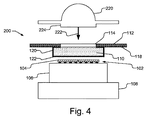
- 光を放射する光源と、前記光源から放射光を受け取り、前記放射光を少なくとも部分的に変換し、変換光を生成する波長変換素子と、開口部を持つ不透明な支持構造体とを有する装置であって、
前記波長変換素子が、前記波長変換素子によって生成された前記変換光が前記開口部を通して放射されるように前記開口部と位置合わせされ、前記波長変換素子及び前記支持構造体の重なり合う部分において前記支持構造体に取り付けられ、前記重なり合う部分が反射性であり、
前記波長変換素子の側面が反射コーティングで覆われる装置。 - 前記波長変換素子が、自己支持剛体材料である請求項1に記載の装置。
- 前記波長変換素子が、発光セラミックである請求項1に記載の装置。
- 前記開口部が、前記支持構造体を通る穴である請求項1に記載の装置。
- 前記支持構造体が、前記開口部を規定する反射層で覆われる透明材料から形成される請求項1に記載の装置。
- 前記開口部に結合される光学素子を更に有する請求項1に記載の装置。
- 前記光学素子が、前記開口部を介して前記波長変換素子に取り付けられる請求項6に記載の装置。
- 前記光学素子が、前記支持構造体及び前記開口部と一体的に形成される請求項6に記載の装置。
- 前記開口部を位置合わせのために用いて前記支持構造体に取り付けられる光学素子を更に有する請求項1に記載の装置。
- 前記光源が少なくとも1つの発光ダイオードを有する請求項1に記載の装置。
- 基板を更に有し、前記少なくとも1つの発光ダイオードが、前記基板に結合され、前記支持構造体が、前記基板に結合される請求項9に記載の装置。
- ヒートシンクを更に有し、前記少なくとも1つの発光ダイオードが、前記ヒートシンクに結合され、前記支持構造体が、前記ヒートシンクに結合される請求項9に記載の装置。
- 前記支持構造体が、前記波長変換素子を、前記波長変換素子が前記光源と物理的に接触しないように保持する請求項1に記載の装置。
- 前記支持構造体が、前記波長変換素子を、前記波長変換素子が前記光源と物理的に接触するように保持する請求項1に記載の装置。
- 前記波長変換素子上に反射防止コーティングを更に有し、前記反射防止コーティングが、前記波長変換素子と前記光源との間に位置する請求項1に記載の装置。
- 光を放射する少なくとも1つの発光ダイオードを含む光源と、前記光源から放射光を受け取り、前記放射光を少なくとも部分的に変換し、変換光を生成する発光セラミックと、開口部を持つ不透明な支持構造体とを有する装置であって、
前記発光セラミックが、前記発光セラミックによって生成された前記変換光が前記開口部を通して放射されるように前記開口部と位置合わせされ、前記発光セラミック及び前記支持構造体の重なり合う部分において前記支持構造体に取り付けられ、前記重なり合う部分が反射性であり、
前記発光セラミックの側面が反射コーティングで覆われる装置。 - 前記開口部が、前記支持構造体を通る穴である請求項16に記載の装置。
- 前記支持構造体が、前記開口部を規定する反射層で覆われる透明材料から形成される請求項16に記載の装置。
- 前記開口部に結合される光学素子を更に有する請求項16に記載の装置。
- 前記光学素子が、前記開口部を介して前記発光セラミックに取り付けられる請求項19に記載の装置。
- 前記光学素子が、前記支持構造体及び前記開口部と一体的に形成される請求項19に記載の装置。
- 前記開口部を位置合わせのために用いて前記支持構造体に取り付けられる光学素子を更に有する請求項16に記載の装置。
- 前記支持構造体が、前記発光セラミックを、前記発光セラミックが前記光源と物理的に接触しないように保持する請求項16に記載の装置。
- 前記支持構造体が、前記発光セラミックを、前記発光セラミックが前記光源と物理的に接触するように保持する請求項16に記載の装置。
- 前記発光セラミック上に反射防止コーティングを更に有し、前記反射防止コーティングが、前記発光セラミックと前記光源との間に位置する請求項16に記載の装置。
Applications Claiming Priority (3)
| Application Number | Priority Date | Filing Date | Title |
|---|---|---|---|
| US11/754,210 US7700967B2 (en) | 2007-05-25 | 2007-05-25 | Illumination device with a wavelength converting element held by a support structure having an aperture |
| US11/754,210 | 2007-05-25 | ||
| PCT/IB2008/051999 WO2008146200A1 (en) | 2007-05-25 | 2008-05-21 | Illumination device with a wavelength converting element held by a support structure having an aperture |
Publications (3)
| Publication Number | Publication Date |
|---|---|
| JP2010528467A JP2010528467A (ja) | 2010-08-19 |
| JP2010528467A5 JP2010528467A5 (ja) | 2013-05-23 |
| JP5439365B2 true JP5439365B2 (ja) | 2014-03-12 |
Family
ID=39761868
Family Applications (1)
| Application Number | Title | Priority Date | Filing Date |
|---|---|---|---|
| JP2010508955A Active JP5439365B2 (ja) | 2007-05-25 | 2008-05-21 | 開口部を持つ支持構造体によって保持される波長変換素子を備える照明装置 |
Country Status (9)
| Country | Link |
|---|---|
| US (1) | US7700967B2 (ja) |
| EP (1) | EP2162925B1 (ja) |
| JP (1) | JP5439365B2 (ja) |
| KR (1) | KR101477474B1 (ja) |
| CN (1) | CN101711435B (ja) |
| BR (1) | BRPI0812044B1 (ja) |
| RU (1) | RU2470413C2 (ja) |
| TW (1) | TWI446592B (ja) |
| WO (1) | WO2008146200A1 (ja) |
Families Citing this family (27)
| Publication number | Priority date | Publication date | Assignee | Title |
|---|---|---|---|---|
| EP2346101A4 (en) * | 2008-10-15 | 2015-11-25 | Koito Mfg Co Ltd | LIGHT-EMITTING MODULE, MANUFACTURING METHOD FOR A LIGHT-EMITTING MODULE AND LIGHTING BODY |
| DE102009003936B4 (de) * | 2009-01-05 | 2011-02-24 | Siemens Aktiengesellschaft | Licht emittierendes Bauelement mit einer Konverterkeramik und einer Kühleinrichtung |
| WO2010131402A1 (ja) * | 2009-05-15 | 2010-11-18 | 株式会社小糸製作所 | 発光モジュール、発光モジュールの製造方法、および灯具ユニット |
| US9547119B2 (en) | 2009-07-14 | 2017-01-17 | Philips Lighting Holding B.V. | Color temperature variable light emitter |
| US8936377B2 (en) * | 2010-03-31 | 2015-01-20 | Alcon Research, Ltd. | Apparatus for enhancing brightness of a wavelength converting element |
| CN102376842A (zh) * | 2010-08-11 | 2012-03-14 | 亿广科技(上海)有限公司 | 发光二极管封装结构 |
| US20120119241A1 (en) * | 2010-11-17 | 2012-05-17 | Luminus Devices, Inc. | Etendue and Light Extraction System and Method |
| KR101878270B1 (ko) * | 2011-09-15 | 2018-07-13 | 엘지이노텍 주식회사 | 광여기 판을 포함하는 조명 장치 및 광여기 테이프 |
| DE102012005654B4 (de) * | 2011-10-25 | 2021-03-04 | Schott Ag | Optischer Konverter für hohe Leuchtdichten |
| DE102012005657B4 (de) * | 2012-03-22 | 2020-06-10 | Schott Ag | Weißlichtbeleuchtungsvorrichtung |
| JP6089686B2 (ja) * | 2012-12-25 | 2017-03-08 | 日亜化学工業株式会社 | 発光装置 |
| JP6075712B2 (ja) * | 2013-03-25 | 2017-02-08 | ウシオ電機株式会社 | 発光デバイス |
| DE102013013296B4 (de) * | 2013-08-12 | 2020-08-06 | Schott Ag | Konverter-Kühlkörperverbund mit metallischer Lotverbindung und Verfahren zu dessen Herstellung |
| CN104566229B (zh) * | 2013-10-15 | 2016-06-08 | 深圳市光峰光电技术有限公司 | 波长转换装置的制造方法 |
| TWI517450B (zh) * | 2013-10-21 | 2016-01-11 | 隆達電子股份有限公司 | 發光二極體封裝體 |
| KR20170002618A (ko) * | 2014-05-15 | 2017-01-06 | 쓰리엠 이노베이티브 프로퍼티즈 컴파니 | 반사성 기판 상의 가요성 회로 |
| JP2016018921A (ja) * | 2014-07-09 | 2016-02-01 | 日本電気硝子株式会社 | 波長変換部材及び発光デバイス |
| US10211187B2 (en) | 2014-07-18 | 2019-02-19 | Koninklijke Philips N.V. | Light emitting diodes and reflector |
| KR102556681B1 (ko) * | 2015-03-30 | 2023-07-18 | 코닌클리케 필립스 엔.브이. | 고휘도 발광 디바이스들을 위한 주변 히트 싱크 배열 |
| JP6332294B2 (ja) * | 2015-11-30 | 2018-05-30 | 日亜化学工業株式会社 | 発光装置 |
| JP6955135B2 (ja) | 2016-10-19 | 2021-10-27 | 日亜化学工業株式会社 | 発光装置およびその製造方法 |
| WO2018199901A1 (en) * | 2017-04-24 | 2018-11-01 | Hewlett-Packard Development Company, L.P. | Micro light-emitting diode display with 3d orifice plating and light filtering |
| KR102405589B1 (ko) * | 2017-05-26 | 2022-06-08 | 쑤저우 레킨 세미컨덕터 컴퍼니 리미티드 | 반도체소자 |
| JP2019028096A (ja) * | 2017-07-25 | 2019-02-21 | 日本電気硝子株式会社 | 波長変換部材 |
| DE102017129623B4 (de) * | 2017-12-12 | 2024-03-28 | OSRAM Opto Semiconductors Gesellschaft mit beschränkter Haftung | Licht emittierendes Halbleiterbauelement |
| JP6888129B2 (ja) * | 2019-02-21 | 2021-06-16 | シャープ株式会社 | 発光装置 |
| JP2020136671A (ja) * | 2019-02-21 | 2020-08-31 | シャープ株式会社 | 発光装置 |
Family Cites Families (22)
| Publication number | Priority date | Publication date | Assignee | Title |
|---|---|---|---|---|
| JPS6273560U (ja) * | 1985-10-24 | 1987-05-11 | ||
| US6504301B1 (en) * | 1999-09-03 | 2003-01-07 | Lumileds Lighting, U.S., Llc | Non-incandescent lightbulb package using light emitting diodes |
| US6357889B1 (en) * | 1999-12-01 | 2002-03-19 | General Electric Company | Color tunable light source |
| JP3614776B2 (ja) * | 2000-12-19 | 2005-01-26 | シャープ株式会社 | チップ部品型ledとその製造方法 |
| EP1672707B1 (en) * | 2001-04-20 | 2019-07-31 | Nichia Corporation | Light emitting device |
| JP2002344029A (ja) * | 2001-05-17 | 2002-11-29 | Rohm Co Ltd | 発光ダイオードの色調調整方法 |
| JP2003110146A (ja) * | 2001-07-26 | 2003-04-11 | Matsushita Electric Works Ltd | 発光装置 |
| JP4009828B2 (ja) * | 2002-03-22 | 2007-11-21 | 日亜化学工業株式会社 | 窒化物蛍光体及びその製造方法 |
| JP3707688B2 (ja) * | 2002-05-31 | 2005-10-19 | スタンレー電気株式会社 | 発光装置およびその製造方法 |
| JP2004031101A (ja) * | 2002-06-25 | 2004-01-29 | Tdk Corp | 発光素子及び発光パネル |
| US7038370B2 (en) * | 2003-03-17 | 2006-05-02 | Lumileds Lighting, U.S., Llc | Phosphor converted light emitting device |
| JP2004349646A (ja) * | 2003-05-26 | 2004-12-09 | Matsushita Electric Works Ltd | 発光装置 |
| US7482638B2 (en) | 2003-08-29 | 2009-01-27 | Philips Lumileds Lighting Company, Llc | Package for a semiconductor light emitting device |
| WO2005097938A1 (ja) * | 2004-03-31 | 2005-10-20 | Nippon Electric Glass Co., Ltd. | 蛍光体及び発光ダイオード |
| US7361938B2 (en) * | 2004-06-03 | 2008-04-22 | Philips Lumileds Lighting Company Llc | Luminescent ceramic for a light emitting device |
| WO2006001316A1 (ja) * | 2004-06-24 | 2006-01-05 | Ube Industries, Ltd. | 白色発光ダイオード装置 |
| US20060124953A1 (en) * | 2004-12-14 | 2006-06-15 | Negley Gerald H | Semiconductor light emitting device mounting substrates and packages including cavities and cover plates, and methods of packaging same |
| JP4866003B2 (ja) | 2004-12-22 | 2012-02-01 | パナソニック電工株式会社 | 発光装置 |
| EP1875781B1 (en) * | 2005-04-20 | 2008-10-08 | Philips Intellectual Property & Standards GmbH | Illumination system comprising a ceramic luminescence converter |
| JP4894186B2 (ja) | 2005-07-26 | 2012-03-14 | 日本電気硝子株式会社 | 蛍光体及び発光ダイオード |
| RU53500U1 (ru) * | 2005-11-22 | 2006-05-10 | Емельян Михайлович Гамарц | Электролюминесцентный излучатель |
| US7663152B2 (en) * | 2006-08-09 | 2010-02-16 | Philips Lumileds Lighting Company, Llc | Illumination device including wavelength converting element side holding heat sink |
-
2007
- 2007-05-25 US US11/754,210 patent/US7700967B2/en active Active
-
2008
- 2008-05-19 TW TW097118395A patent/TWI446592B/zh active
- 2008-05-21 WO PCT/IB2008/051999 patent/WO2008146200A1/en active Application Filing
- 2008-05-21 BR BRPI0812044A patent/BRPI0812044B1/pt active IP Right Grant
- 2008-05-21 CN CN2008800175121A patent/CN101711435B/zh active Active
- 2008-05-21 KR KR1020097027125A patent/KR101477474B1/ko active IP Right Grant
- 2008-05-21 RU RU2009148312/28A patent/RU2470413C2/ru active
- 2008-05-21 JP JP2010508955A patent/JP5439365B2/ja active Active
- 2008-05-21 EP EP08751277.8A patent/EP2162925B1/en active Active
Also Published As
| Publication number | Publication date |
|---|---|
| KR101477474B1 (ko) | 2014-12-30 |
| BRPI0812044A2 (pt) | 2017-03-21 |
| US20080290362A1 (en) | 2008-11-27 |
| TW200913319A (en) | 2009-03-16 |
| WO2008146200A1 (en) | 2008-12-04 |
| JP2010528467A (ja) | 2010-08-19 |
| US7700967B2 (en) | 2010-04-20 |
| EP2162925B1 (en) | 2014-07-16 |
| RU2009148312A (ru) | 2011-06-27 |
| TWI446592B (zh) | 2014-07-21 |
| RU2470413C2 (ru) | 2012-12-20 |
| EP2162925A1 (en) | 2010-03-17 |
| CN101711435B (zh) | 2011-09-28 |
| CN101711435A (zh) | 2010-05-19 |
| BRPI0812044B1 (pt) | 2018-11-13 |
| KR20100017930A (ko) | 2010-02-16 |
Similar Documents
| Publication | Publication Date | Title |
|---|---|---|
| JP5439365B2 (ja) | 開口部を持つ支持構造体によって保持される波長変換素子を備える照明装置 | |
| RU2581426C2 (ru) | Светоизлучающий модуль, лампа, осветительное устройство и устройство отображения | |
| KR101193990B1 (ko) | 투명 열 전도성 층을 구비한 발광 디바이스 | |
| US7842960B2 (en) | Light emitting packages and methods of making same | |
| JP6531030B2 (ja) | 制御された角度の非一様性を備えるled | |
| JP5743548B2 (ja) | 照明装置 | |
| US20100133555A1 (en) | Solid metal block semiconductor light emitting device mounting substrates | |
| US20080203911A1 (en) | Light Source With Glass Housing | |
| CN103797597A (zh) | 发光模块、灯、照明器和显示装置 | |
| CN102217099A (zh) | 具有耐熔荧光层的发光器件 | |
| WO2011016295A1 (ja) | 発光装置及び発光装置の製造方法 | |
| EP2743999A2 (en) | Light emitting device package including phosphor film, method of manufacturing the same, and lighting apparatus using the same | |
| KR20210041539A (ko) | 인광체 조명 시스템에 대한 반사 컬러 보정 | |
| JP2008078225A (ja) | 発光装置 | |
| US9753357B2 (en) | Compact solid-state camera flash | |
| JP4868960B2 (ja) | 発光装置およびその製造方法 | |
| JP7339518B2 (ja) | 発光モジュールの製造方法 | |
| WO2016163520A1 (ja) | 発光装置、照明装置、及び発光装置の製造方法 | |
| JP5561296B2 (ja) | 発光装置 | |
| JP5291162B2 (ja) | 発光装置およびその製造方法 | |
| JP2018006704A (ja) | 発光装置および照明装置 |
Legal Events
| Date | Code | Title | Description |
|---|---|---|---|
| A621 | Written request for application examination |
Free format text: JAPANESE INTERMEDIATE CODE: A621 Effective date: 20110427 |
|
| A977 | Report on retrieval |
Free format text: JAPANESE INTERMEDIATE CODE: A971007 Effective date: 20121031 |
|
| A131 | Notification of reasons for refusal |
Free format text: JAPANESE INTERMEDIATE CODE: A131 Effective date: 20130108 |
|
| A524 | Written submission of copy of amendment under article 19 pct |
Free format text: JAPANESE INTERMEDIATE CODE: A524 Effective date: 20130405 |
|
| A131 | Notification of reasons for refusal |
Free format text: JAPANESE INTERMEDIATE CODE: A131 Effective date: 20130725 |
|
| A521 | Request for written amendment filed |
Free format text: JAPANESE INTERMEDIATE CODE: A523 Effective date: 20131022 |
|
| TRDD | Decision of grant or rejection written | ||
| A01 | Written decision to grant a patent or to grant a registration (utility model) |
Free format text: JAPANESE INTERMEDIATE CODE: A01 Effective date: 20131119 |
|
| A61 | First payment of annual fees (during grant procedure) |
Free format text: JAPANESE INTERMEDIATE CODE: A61 Effective date: 20131216 |
|
| R150 | Certificate of patent or registration of utility model |
Free format text: JAPANESE INTERMEDIATE CODE: R150 Ref document number: 5439365 Country of ref document: JP Free format text: JAPANESE INTERMEDIATE CODE: R150 |
|
| R250 | Receipt of annual fees |
Free format text: JAPANESE INTERMEDIATE CODE: R250 |
|
| R250 | Receipt of annual fees |
Free format text: JAPANESE INTERMEDIATE CODE: R250 |
|
| R250 | Receipt of annual fees |
Free format text: JAPANESE INTERMEDIATE CODE: R250 |
|
| S111 | Request for change of ownership or part of ownership |
Free format text: JAPANESE INTERMEDIATE CODE: R313113 |
|
| S533 | Written request for registration of change of name |
Free format text: JAPANESE INTERMEDIATE CODE: R313533 |
|
| R350 | Written notification of registration of transfer |
Free format text: JAPANESE INTERMEDIATE CODE: R350 |
|
| R250 | Receipt of annual fees |
Free format text: JAPANESE INTERMEDIATE CODE: R250 |
|
| R250 | Receipt of annual fees |
Free format text: JAPANESE INTERMEDIATE CODE: R250 |
|
| R250 | Receipt of annual fees |
Free format text: JAPANESE INTERMEDIATE CODE: R250 |
|
| R250 | Receipt of annual fees |
Free format text: JAPANESE INTERMEDIATE CODE: R250 |
|
| R250 | Receipt of annual fees |
Free format text: JAPANESE INTERMEDIATE CODE: R250 |