JP5439365B2 - Illumination device comprising a wavelength conversion element held by a support structure having an opening - Google Patents
Illumination device comprising a wavelength conversion element held by a support structure having an opening Download PDFInfo
- Publication number
- JP5439365B2 JP5439365B2 JP2010508955A JP2010508955A JP5439365B2 JP 5439365 B2 JP5439365 B2 JP 5439365B2 JP 2010508955 A JP2010508955 A JP 2010508955A JP 2010508955 A JP2010508955 A JP 2010508955A JP 5439365 B2 JP5439365 B2 JP 5439365B2
- Authority
- JP
- Japan
- Prior art keywords
- support structure
- opening
- wavelength conversion
- conversion element
- light source
- Prior art date
- Legal status (The legal status is an assumption and is not a legal conclusion. Google has not performed a legal analysis and makes no representation as to the accuracy of the status listed.)
- Active
Links
- 238000006243 chemical reaction Methods 0.000 title claims description 43
- 238000005286 illumination Methods 0.000 title description 7
- 239000000919 ceramic Substances 0.000 claims description 30
- 230000003287 optical effect Effects 0.000 claims description 22
- 239000000463 material Substances 0.000 claims description 14
- 239000011248 coating agent Substances 0.000 claims description 11
- 238000000576 coating method Methods 0.000 claims description 11
- 239000006117 anti-reflective coating Substances 0.000 claims description 5
- 239000012780 transparent material Substances 0.000 claims description 5
- 239000000758 substrate Substances 0.000 claims description 4
- OAICVXFJPJFONN-UHFFFAOYSA-N Phosphorus Chemical compound [P] OAICVXFJPJFONN-UHFFFAOYSA-N 0.000 description 16
- 239000002245 particle Substances 0.000 description 7
- 239000011230 binding agent Substances 0.000 description 5
- 229910052782 aluminium Inorganic materials 0.000 description 4
- XAGFODPZIPBFFR-UHFFFAOYSA-N aluminium Chemical compound [Al] XAGFODPZIPBFFR-UHFFFAOYSA-N 0.000 description 4
- 238000000926 separation method Methods 0.000 description 4
- 239000004065 semiconductor Substances 0.000 description 3
- 239000004593 Epoxy Substances 0.000 description 2
- 229920000106 Liquid crystal polymer Polymers 0.000 description 2
- 239000004977 Liquid-crystal polymers (LCPs) Substances 0.000 description 2
- 239000002223 garnet Substances 0.000 description 2
- 239000011521 glass Substances 0.000 description 2
- 238000010438 heat treatment Methods 0.000 description 2
- 230000005855 radiation Effects 0.000 description 2
- 229920005989 resin Polymers 0.000 description 2
- 239000011347 resin Substances 0.000 description 2
- 229910052710 silicon Inorganic materials 0.000 description 2
- 239000010703 silicon Substances 0.000 description 2
- 239000010409 thin film Substances 0.000 description 2
- RYGMFSIKBFXOCR-UHFFFAOYSA-N Copper Chemical compound [Cu] RYGMFSIKBFXOCR-UHFFFAOYSA-N 0.000 description 1
- 229910004283 SiO 4 Inorganic materials 0.000 description 1
- 229910004122 SrSi Inorganic materials 0.000 description 1
- 239000003086 colorant Substances 0.000 description 1
- 229910052802 copper Inorganic materials 0.000 description 1
- 239000010949 copper Substances 0.000 description 1
- 230000008878 coupling Effects 0.000 description 1
- 238000010168 coupling process Methods 0.000 description 1
- 238000005859 coupling reaction Methods 0.000 description 1
- 125000003700 epoxy group Chemical group 0.000 description 1
- 239000010408 film Substances 0.000 description 1
- 238000003754 machining Methods 0.000 description 1
- QSHDDOUJBYECFT-UHFFFAOYSA-N mercury Chemical compound [Hg] QSHDDOUJBYECFT-UHFFFAOYSA-N 0.000 description 1
- 229910052753 mercury Inorganic materials 0.000 description 1
- 229910052751 metal Inorganic materials 0.000 description 1
- 239000002184 metal Substances 0.000 description 1
- 229910001092 metal group alloy Inorganic materials 0.000 description 1
- 230000004048 modification Effects 0.000 description 1
- 238000012986 modification Methods 0.000 description 1
- 238000000465 moulding Methods 0.000 description 1
- 239000004038 photonic crystal Substances 0.000 description 1
- 229920000647 polyepoxide Polymers 0.000 description 1
- 229920001296 polysiloxane Polymers 0.000 description 1
- 239000000843 powder Substances 0.000 description 1
- 229920006395 saturated elastomer Polymers 0.000 description 1
- 229910052709 silver Inorganic materials 0.000 description 1
- 239000004332 silver Substances 0.000 description 1
- 229910000679 solder Inorganic materials 0.000 description 1
- 229910052724 xenon Inorganic materials 0.000 description 1
- FHNFHKCVQCLJFQ-UHFFFAOYSA-N xenon atom Chemical compound [Xe] FHNFHKCVQCLJFQ-UHFFFAOYSA-N 0.000 description 1
Images


Classifications
-
- H—ELECTRICITY
- H01—ELECTRIC ELEMENTS
- H01L—SEMICONDUCTOR DEVICES NOT COVERED BY CLASS H10
- H01L33/00—Semiconductor devices with at least one potential-jump barrier or surface barrier specially adapted for light emission; Processes or apparatus specially adapted for the manufacture or treatment thereof or of parts thereof; Details thereof
- H01L33/48—Semiconductor devices with at least one potential-jump barrier or surface barrier specially adapted for light emission; Processes or apparatus specially adapted for the manufacture or treatment thereof or of parts thereof; Details thereof characterised by the semiconductor body packages
- H01L33/50—Wavelength conversion elements
- H01L33/507—Wavelength conversion elements the elements being in intimate contact with parts other than the semiconductor body or integrated with parts other than the semiconductor body
-
- H—ELECTRICITY
- H01—ELECTRIC ELEMENTS
- H01L—SEMICONDUCTOR DEVICES NOT COVERED BY CLASS H10
- H01L33/00—Semiconductor devices with at least one potential-jump barrier or surface barrier specially adapted for light emission; Processes or apparatus specially adapted for the manufacture or treatment thereof or of parts thereof; Details thereof
- H01L33/48—Semiconductor devices with at least one potential-jump barrier or surface barrier specially adapted for light emission; Processes or apparatus specially adapted for the manufacture or treatment thereof or of parts thereof; Details thereof characterised by the semiconductor body packages
- H01L33/58—Optical field-shaping elements
-
- H—ELECTRICITY
- H01—ELECTRIC ELEMENTS
- H01L—SEMICONDUCTOR DEVICES NOT COVERED BY CLASS H10
- H01L33/00—Semiconductor devices with at least one potential-jump barrier or surface barrier specially adapted for light emission; Processes or apparatus specially adapted for the manufacture or treatment thereof or of parts thereof; Details thereof
- H01L33/48—Semiconductor devices with at least one potential-jump barrier or surface barrier specially adapted for light emission; Processes or apparatus specially adapted for the manufacture or treatment thereof or of parts thereof; Details thereof characterised by the semiconductor body packages
- H01L33/483—Containers
-
- Y—GENERAL TAGGING OF NEW TECHNOLOGICAL DEVELOPMENTS; GENERAL TAGGING OF CROSS-SECTIONAL TECHNOLOGIES SPANNING OVER SEVERAL SECTIONS OF THE IPC; TECHNICAL SUBJECTS COVERED BY FORMER USPC CROSS-REFERENCE ART COLLECTIONS [XRACs] AND DIGESTS
- Y10—TECHNICAL SUBJECTS COVERED BY FORMER USPC
- Y10S—TECHNICAL SUBJECTS COVERED BY FORMER USPC CROSS-REFERENCE ART COLLECTIONS [XRACs] AND DIGESTS
- Y10S362/00—Illumination
- Y10S362/80—Light emitting diode
Description
本発明は、照明装置に関し、とりわけ、半導体発光装置などの高放射輝度光源によって生成される光の波長変換に関する。 The present invention relates to a lighting device, and more particularly to wavelength conversion of light generated by a high radiance light source such as a semiconductor light emitting device.
多くの照明用途において、発光ダイオード(LED)を用いる照明装置がだんだん一般的になっている。一般に、LEDは、白色光を生成するために一次発光の蛍光体変換を用いるが、蛍光体は、赤色、緑色及び黄色のようなより多くの飽和色を作成するためにも用いられ得る。 In many lighting applications, lighting devices that use light emitting diodes (LEDs) are becoming increasingly common. In general, LEDs use primary emission phosphor conversion to produce white light, but phosphors can also be used to create more saturated colors such as red, green and yellow.
蛍光体をLEDと物理的に接触させる従来の装置には、結合温度範囲が限られるなどの不利な点がある。更に、結合材の選択は、コストに影響を及ぼし得るばかりでなく、例えば、熱的に誘導される機械的応力に起因して、信頼性にも影響を及ぼし得る。したがって、改善が望ましい。 Conventional devices that physically contact the phosphor with the LED have disadvantages such as a limited bonding temperature range. Furthermore, the choice of binder can not only affect the cost, but can also affect reliability, for example due to thermally induced mechanical stress. Improvement is therefore desirable.
本発明の実施例によれば、照明装置は、1つ以上の発光ダイオードなどの光源と、不透明な支持構造体に取り付けられる波長変換素子とを含む。前記支持構造体は、開口部を含み、前記波長変換素子は、変換光が前記開口部を通して放射されるように前記開口部と位置合わせされる。前記波長変換素子は、発光セラミックなどの硬い構造体であってもよく、前記開口部は、前記支持構造体を通る穴であってもよい。前記支持構造体は、前記波長変換素子を、前記波長変換素子が前記光源から物理的に分離されるように保持してもよく、又は他の例においては、前記支持構造体は、前記波長変換素子を前記光源と物理的に接触させてもよい。 According to an embodiment of the present invention, the lighting device includes one or more light sources such as light emitting diodes and a wavelength converting element attached to the opaque support structure. The support structure includes an opening, and the wavelength conversion element is aligned with the opening such that converted light is emitted through the opening. The wavelength conversion element may be a hard structure such as a luminescent ceramic, and the opening may be a hole that passes through the support structure. The support structure may hold the wavelength conversion element such that the wavelength conversion element is physically separated from the light source, or in another example, the support structure may include the wavelength conversion element. The element may be in physical contact with the light source.
本発明の実施例によれば、照明装置の波長変換素子は、開口部であって、変換された光が前記開口部を通して放射されてもよく、必要に応じて、ポンプ光の一部が前記開口部を通して放射されてもよい開口部を含む構造体によって物理的に支持される。 According to the embodiment of the present invention, the wavelength conversion element of the illumination device may be an opening, and the converted light may be emitted through the opening, and a part of the pump light may be emitted as necessary. It is physically supported by a structure that includes an opening that may be emitted through the opening.
図1は、本発明の或る実施例による照明装置100を図示する側面図である。照明装置100は光源102を含む。前記光源102は、例えば、1つ以上の発光ダイオード(LED)104などの半導体発光装置、又はキセノンランプ若しくは水銀ランプなどの短波長光を生成することができる他のタイプの光源であり得る。LED104は、例えば、青色又は紫外線(UV)LEDであり、本開示と同じ譲受人を持つ、2003年8月29日に出願されたFrank Wal他による"Package for a Semiconductor Light Emitting Device"という題名の米国シリアル番号第10/652,348号、公開公報第2005/0045901号に記載されているタイプのような高放射輝度装置であってもよい。この文献は、参照により本願明細書に盛り込まれる。LED104の角度放射パターンは、ランバート放射パターンであり得る、又は格子構造などのフォトニック結晶を用いて制御され得る。発光ダイオード104は、サブマウント106に取り付けられるように図示されている。前記サブマウント106は、例えば、セラミック又はシリコンであってもよく、LED104のための必要な電気的接触を含み得る。サブマウント106は、ヒートシンク108に取り付けられてもよい。必要に応じて、サブマウント106及びヒートシンク108以外の支持構造体が用いられてもよい。
FIG. 1 is a side view illustrating a
照明装置100は、支持構造体112に取り付けられ、支持構造体112によって保持される波長変換素子110を含み、前記支持構造体112は、開口部114を含む。図1には示されていないが、支持構造体112は、後述するように、照明装置の様々な部分に、物理的に、取り付けられ得る、又は接続され得る。開口部114は、波長変換素子110からの順方向放射光(及びLED104からの、波長変換素子110を通過するあらゆるポンプ光)を伝達するよう、波長変換素子119の上に配置される或る実施例においては、支持構造体112は、開口部114が支持構造体112を通る穴であるように製造され得る。前記支持構造体112は、スタンピング、モールディング又は機械加工よって不透明材料から製造され得る。支持構造体112は、一例として、アルミニウム、銅又は他の適切な材料などの金属又は金属合金から製造され得る。波長変換素子110は、例えば、エポキシ、ガラス、はんだ又は他の適切な材料によって、支持構造体112の重なり合う部分116に取り付けられる。別の実施例においては、支持構造体112は、例えば、波長変換素子110が取り付けられる面118を、反射材料で被覆される透明材料、例えば、LCP(液晶ポリマ)ガラス、シリコン又は他の適切な材料から製造され得る。このような実施例においては、開口部114は、反射材料がないことによって規定される。
The
波長変換素子110を光源102に向かい合うように支持構造体112に取り付けることによって、照明装置100の組立体は、簡単にされ、LED104を大きな温度逸脱にさらさないようにする。更に、支持構造体112は、青色光の漏れを阻止し、波長変換素子110は、多数のダイからの光と混ぜ合わせ、場合によっては、見かけ上連続した光源を供給する。
By attaching the
或る実施例においては、波長変換素子110からの側面放射光を再利用するために、波長変換素子110の側面は、アルミニウム、銀若しくは3MのESR反射フィルム、又は任意の他の適切な反射材料の層などの反射コーティング120で覆われ得る。更に、支持構造体112及び/又は結合材の重なり合う部分116は、開口部114を通して放射されない光の再利用を向上させるために反射性であり得る。
In some embodiments, the side surface of the
とりわけ、開口部114が支持構造体112を通る穴として形成される実施例においては、波長変換素子110は、硬い材料から形成され得る。波長変換素子110は、一例として、本願明細書では時として「発光セラミック」と呼ぶセラミックスラブであってもよい。セラミックスラブは、一般に、自己支持層であり、特定の波長に対して半透明又は透明であり得る。このことは、共形層などの不透明波長変換層と関連する散乱損失を減らし得る。発光セラミック層は、薄膜又は共形蛍光体層よりロバストであり得る。実施例によっては、波長変換素子110、例えば結合材中の蛍光体として、発光セラミック以外の材料が用いられ得る。
In particular, in embodiments where the
発光セラミック層にされ得る蛍光体の例は、黄色−緑色領域内の光を放射するLu3Al5O12:Ce3+及びY3Al5O12:Ce3+などの一般式(Lu1-x-y-a-bYxGdy)3(Al1-zGaz)5O12:CeaPrbを備え、ここで、0<x<1、0<y<1、0<z≦0.1、0<a≦0.2且つ0<b≦0.1であるアルミニウムガーネット蛍光体と、赤色領域内の光を放射するSr2Si5N8:Eu2+などの一般式(Sr1-x-yBaxCay)2-zSi5-aAlaN8-a0a:Euz 2+を備え、ここで、0≦a<5、0<x≦1、0≦y≦1且つ0<z≦1であるアルミニウムガーネット蛍光体とを含む。適切なY3Al5O12:Ce3+セラミックスラブは、ノースカロライナ州シャーロットのBaikowski International Corporationから購入され得る。例えばSrSi2N2O2:Eu2+を含む(Sr1-a-bCabBac)SixNyOz:Eua 2+(a=0.002乃至0.2、b=0.0乃至0.25、c=0.0乃至0.25、x=1.5乃至2.5、z=1.5乃至2.5)と、例えばSrGa2S4:Eu2+を含む(Sr1-u-v-xMguCavBax)(Ga2-y-zAlyInzS4):Eu2+と、Sr1-xBaxSiO4:Eu2+と、例えばCaS:Eu2+及びSrS:Eu2+を含む(Ca1-xSrx)S:Eu2+(0<x≦1)とを含む他の緑色、黄色及び赤色も適切であり得る。 Examples of phosphors that can be made into luminescent ceramic layers include general formulas such as Lu 3 Al 5 O 12 : Ce 3+ and Y 3 Al 5 O 12 : Ce 3+ that emit light in the yellow-green region (Lu 1 -xyab Y x Gd y ) 3 (Al 1 -z Ga z ) 5 O 12 : Ce a Pr b , where 0 <x <1, 0 <y <1, 0 <z ≦ 0.1, Aluminum garnet phosphors with 0 <a ≦ 0.2 and 0 <b ≦ 0.1, and general formulas such as Sr 2 Si 5 N 8 : Eu 2+ that emit light in the red region (Sr 1-xy Ba x Ca y ) 2-z Si 5-a Al a N 8-a 0 a : Eu z 2+ where 0 ≦ a <5, 0 <x ≦ 1, 0 ≦ y ≦ 1 and 0 And an aluminum garnet phosphor satisfying <z ≦ 1. Suitable Y 3 Al 5 O 12 : Ce 3+ ceramic slabs can be purchased from Baikowski International Corporation, Charlotte, NC. For example, (Sr 1-ab Ca b Ba c ) Si x N y O z : Eu a 2+ (a = 0.002 to 0.2, b = 0.0 containing SrSi 2 N 2 O 2 : Eu 2+ To 0.25, c = 0.0 to 0.25, x = 1.5 to 2.5, z = 1.5 to 2.5), and for example, SrGa 2 S 4 : Eu 2+ (Sr 1-uvx Mg u Ca v Ba x) (Ga 2-yz Al y In z S 4): and Eu 2+, Sr 1-x Ba x SiO 4: Eu 2+ and, for example, CaS: Eu 2+ and SrS : including Eu 2+ (Ca 1-x Sr x) S: Eu 2+ (0 <x ≦ 1) and the other green including also yellow and red may be suitable.
発光セラミックは、蛍光体粒子の表面が軟化し始め、溶け始めるまで粉末蛍光体を高圧で加熱することによって形成され得る。部分的に溶けた粒子は、くっつき合って粒子の硬いかたまりを形成する。発光セラミックは、光学的に、光学的な不連続性のない単一の大きな蛍光体粒子として振る舞う薄膜とは異なり、異なる蛍光体粒子間の境界面に小さな光学的な不連続性があるような密集している別々の蛍光体粒子として振る舞う。したがって、発光セラミックは、光学的にほぼ均質であり、発光セラミックを形成する蛍光体材料と同じ屈折率を持つ。発光セラミックは、樹脂などの透明材料内に配置される蛍光体層又は共形蛍光体層とは異なり、一般に、蛍光体自体以外の(有機樹脂又はエポキシなどの)結合材を必要とせず、故に、個々の蛍光体粒子間の異なる屈折率の空間又は材料はごくわずかしかない。結果として、発光セラミックは、共形蛍光体層とは異なり、透明又は半透明である。本発明で用いられ得る発光セラミックに関するより多くの情報については、米国特許出願公開公報第2005/0269582号を参照されたい。この文献は、参照により本願明細書に盛り込まれる。 The luminescent ceramic can be formed by heating the powder phosphor at high pressure until the surface of the phosphor particles begins to soften and melt. Partially melted particles stick together to form a hard mass of particles. Luminescent ceramics, unlike thin films that behave optically as single large phosphor particles without optical discontinuities, have small optical discontinuities at the interface between different phosphor particles. It behaves as a dense, discrete phosphor particle. Thus, the luminescent ceramic is optically nearly homogeneous and has the same refractive index as the phosphor material forming the luminescent ceramic. Luminescent ceramics generally do not require binders (such as organic resins or epoxies) other than the phosphor itself, unlike phosphor layers or conformal phosphor layers that are placed in transparent materials such as resins. There is very little space or material of different refractive index between individual phosphor particles. As a result, the luminescent ceramic is transparent or translucent, unlike the conformal phosphor layer. For more information on luminescent ceramics that can be used in the present invention, see US Patent Application Publication No. 2005/0269582. This document is incorporated herein by reference.
波長変換素子110の入力面には反射防止コーティング122が置かれ、故に、波長変換素子110とLED104との間には反射防止コーティング122がある。別の実施例においては、コーティング122は、青色ポンプ光を透過し、波長変換素子110によって変換された光の領域内の波長を反射するダイクロイックフィルタなどの色分解素子であってもよい。色分解素子116は、波長変換素子110の、光源102に面している入力面111に直接付される高角度受理コーティングであってもよい。
An
図1において図示されているように、支持構造体112は、波長変換素子110が、(矢印103によって大まかに図示されている)光路に沿って光源102から物理的に切り離されるように配置され得る。したがって、波長変換素子110(及び反射防止コーティング122)は、光源102と接触していない。波長変換素子110(及び反射防止コーティング122)と光源102との間の媒体は、例えば、空気、ガス又は真空であり得る。したがって、光源102によって放射される光は、光源102と波長変換素子110(及び反射防止コーティング122)との間のギャップを通って進まなければならない。光源102と波長変換素子110との間の物理的分離の長さは、様々であり得るが、或る実施例においては、50μm乃至250μmの範囲内である。或る実施例においては、光源102と波長変換素子110との間の物理的分離は、光源102による波長変換素子110の実質的な伝導加熱を防止するのに十分である。別の実施例においては、光源102と波長変換素子110との間のギャップを埋めるのに、フィルタ、又はシリコーンゲル若しくは他の適切な材料などの結合材が用いられ得る。
As illustrated in FIG. 1, the
図2は、本発明の別の実施例による照明装置150を図示する側面図である。照明装置150は、所定の素子が同じであるように、図1に示されている照明装置100とほぼ同じである。しかしながら、図2において図示されているように、照明装置150の支持構造体112は、波長変換素子110と光源102との間にギャップがないように、即ち、波長変換素子110が、反射防止コーティング122を介して光源102と物理的に接触するように波長変換素子110を保持する。波長変換素子110は、最適な光結合のために望ましい場合には光源102に結合され得る。
FIG. 2 is a side view illustrating a
図3は、照明装置200を図示する側面図である。前記照明装置200は、所定の素子が同じであるように、図1に示されている照明装置100とほぼ同じである。しかしながら、照明装置200は、開口部114内にドームレンズなどの光学素子202を含む。光学素子202は、開口部114を介して波長変換素子110に取り付けられてもよい。他の例においては、支持構造体112が、開口部114を規定するよう反射コーティングを備える透明材料である場合には、光学素子202は、支持構造体112に結合されてもよく、又は支持構造体112と一体的に形成されてもよい。照明装置200の支持構造体112は、図2において図示されているように波長変換素子110を光源102と接触させるよう配置されてもよいことを理解されたい。
FIG. 3 is a side view illustrating the
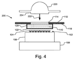
開口部114を備える支持構造体112を用いる利点の1つは、開口部114が、照明装置100に付加的な素子を取り付けるための位置合わせとして用いられることができ、他の例においては、照明装置100を別の構造体に取り付けるための位置合わせとして用いられることができることである。図4は、一例として、矢印222によって図示されているように照明装置100に取り付けられる光学素子220を図示している。光学素子220は、開口部114に嵌合する大きさに作られる突出部224を含む。したがって、開口部114は、光学素子220のための位置合わせの役割を果たす。勿論、他の光学素子又は非光学素子も開口部114を位置合わせのために用い得る。
One advantage of using a
図5は、図3に示されている照明装置200と同様であるが、拡張基板308に取り付けられる支持構造体312を備える照明装置300の側面図を図示している。図6は、図5と同様であるが、光源102のための密閉環境を供給し得る、ヒートシンク356に取り付けられる支持構造体362を持つ照明装置350を備える。
FIG. 5 illustrates a side view of a
教示目的のために、本発明を、特定の実施例に関連して説明しているが、本発明は、これらの特定の実施例に限定されない。本発明の範囲から逸脱せずに、様々な変更及び修正がなされ得る。それ故、添付の請求項の精神及び範囲は、上記の記載に限定されてはならない。 For purposes of teaching, the invention has been described with reference to particular embodiments, but the invention is not limited to these particular embodiments. Various changes and modifications can be made without departing from the scope of the invention. Therefore, the spirit and scope of the appended claims should not be limited to the above description.
Claims (25)
前記波長変換素子が、前記波長変換素子によって生成された前記変換光が前記開口部を通して放射されるように前記開口部と位置合わせされ、前記波長変換素子及び前記支持構造体の重なり合う部分において前記支持構造体に取り付けられ、前記重なり合う部分が反射性であり、
前記波長変換素子の側面が反射コーティングで覆われる装置。 An apparatus comprising: a light source that emits light; a wavelength converting element that receives the emitted light from the light source, at least partially converts the emitted light to generate converted light; and an opaque support structure having an opening. There,
The wavelength conversion element is aligned with the opening so that the converted light generated by the wavelength conversion element is emitted through the opening, and the support is provided at an overlapping portion of the wavelength conversion element and the support structure. Attached to the structure, the overlapping part is reflective;
An apparatus in which a side surface of the wavelength conversion element is covered with a reflective coating.
前記発光セラミックが、前記発光セラミックによって生成された前記変換光が前記開口部を通して放射されるように前記開口部と位置合わせされ、前記発光セラミック及び前記支持構造体の重なり合う部分において前記支持構造体に取り付けられ、前記重なり合う部分が反射性であり、
前記発光セラミックの側面が反射コーティングで覆われる装置。 A light source including at least one light emitting diode that emits light, a luminescent ceramic that receives the emitted light from the light source, at least partially converts the emitted light, and generates converted light, and an opaque support structure having an opening A device having a body,
The luminescent ceramic is aligned with the opening such that the converted light generated by the luminescent ceramic is emitted through the opening, and the luminescent ceramic is placed on the support structure at an overlapping portion of the luminescent ceramic and the support structure. Attached, the overlapping part is reflective,
An apparatus in which a side surface of the luminescent ceramic is covered with a reflective coating.
Applications Claiming Priority (3)
| Application Number | Priority Date | Filing Date | Title |
|---|---|---|---|
| US11/754,210 | 2007-05-25 | ||
| US11/754,210 US7700967B2 (en) | 2007-05-25 | 2007-05-25 | Illumination device with a wavelength converting element held by a support structure having an aperture |
| PCT/IB2008/051999 WO2008146200A1 (en) | 2007-05-25 | 2008-05-21 | Illumination device with a wavelength converting element held by a support structure having an aperture |
Publications (3)
| Publication Number | Publication Date |
|---|---|
| JP2010528467A JP2010528467A (en) | 2010-08-19 |
| JP2010528467A5 JP2010528467A5 (en) | 2013-05-23 |
| JP5439365B2 true JP5439365B2 (en) | 2014-03-12 |
Family
ID=39761868
Family Applications (1)
| Application Number | Title | Priority Date | Filing Date |
|---|---|---|---|
| JP2010508955A Active JP5439365B2 (en) | 2007-05-25 | 2008-05-21 | Illumination device comprising a wavelength conversion element held by a support structure having an opening |
Country Status (9)
| Country | Link |
|---|---|
| US (1) | US7700967B2 (en) |
| EP (1) | EP2162925B1 (en) |
| JP (1) | JP5439365B2 (en) |
| KR (1) | KR101477474B1 (en) |
| CN (1) | CN101711435B (en) |
| BR (1) | BRPI0812044B1 (en) |
| RU (1) | RU2470413C2 (en) |
| TW (1) | TWI446592B (en) |
| WO (1) | WO2008146200A1 (en) |
Families Citing this family (27)
| Publication number | Priority date | Publication date | Assignee | Title |
|---|---|---|---|---|
| WO2010044240A1 (en) * | 2008-10-15 | 2010-04-22 | 株式会社小糸製作所 | Light-emitting module, manufacturing method for light-emitting module, and light fixture unit |
| DE102009003936B4 (en) * | 2009-01-05 | 2011-02-24 | Siemens Aktiengesellschaft | Light-emitting component with a converter ceramic and a cooling device |
| WO2010131402A1 (en) * | 2009-05-15 | 2010-11-18 | 株式会社小糸製作所 | Light-emitting module, method of producing light-emitting module, and lighting fixture unit |
| EP2454753B1 (en) * | 2009-07-14 | 2016-10-05 | Philips Lighting Holding B.V. | Color temperature variable light emitter |
| US8936377B2 (en) * | 2010-03-31 | 2015-01-20 | Alcon Research, Ltd. | Apparatus for enhancing brightness of a wavelength converting element |
| CN102376842A (en) * | 2010-08-11 | 2012-03-14 | 亿广科技(上海)有限公司 | Light emitting diode package structure |
| US20120119241A1 (en) * | 2010-11-17 | 2012-05-17 | Luminus Devices, Inc. | Etendue and Light Extraction System and Method |
| KR101878270B1 (en) * | 2011-09-15 | 2018-07-13 | 엘지이노텍 주식회사 | Lighting device comprising photoluminescent plate and photoluminescent tape |
| DE102012005654B4 (en) * | 2011-10-25 | 2021-03-04 | Schott Ag | Optical converter for high luminance levels |
| DE102012005657B4 (en) * | 2012-03-22 | 2020-06-10 | Schott Ag | White light lighting device |
| JP6089686B2 (en) * | 2012-12-25 | 2017-03-08 | 日亜化学工業株式会社 | Light emitting device |
| JP6075712B2 (en) * | 2013-03-25 | 2017-02-08 | ウシオ電機株式会社 | Light emitting device |
| DE102013013296B4 (en) * | 2013-08-12 | 2020-08-06 | Schott Ag | Converter-heat sink assembly with metallic solder connection and method for its production |
| CN104566229B (en) * | 2013-10-15 | 2016-06-08 | 深圳市光峰光电技术有限公司 | The manufacture method of Wavelength converter |
| TWI517450B (en) * | 2013-10-21 | 2016-01-11 | 隆達電子股份有限公司 | Light emitting diode package |
| SG11201609088VA (en) * | 2014-05-15 | 2016-11-29 | 3M Innovative Properties Co | Flexible circuit on reflective substrate |
| JP2016018921A (en) * | 2014-07-09 | 2016-02-01 | 日本電気硝子株式会社 | Wavelength conversion member and light-emitting device |
| WO2016009088A1 (en) * | 2014-07-18 | 2016-01-21 | Koninklijke Philips N.V. | Light emitting diodes and reflector |
| WO2016156135A1 (en) * | 2015-03-30 | 2016-10-06 | Koninklijke Philips N.V. | Peripheral heat sinking arrangement for high brightness light emitting devices |
| JP6332294B2 (en) * | 2015-11-30 | 2018-05-30 | 日亜化学工業株式会社 | Light emitting device |
| JP6955135B2 (en) | 2016-10-19 | 2021-10-27 | 日亜化学工業株式会社 | Light emitting device and its manufacturing method |
| WO2018199901A1 (en) * | 2017-04-24 | 2018-11-01 | Hewlett-Packard Development Company, L.P. | Micro light-emitting diode display with 3d orifice plating and light filtering |
| KR102405589B1 (en) * | 2017-05-26 | 2022-06-08 | 쑤저우 레킨 세미컨덕터 컴퍼니 리미티드 | Semiconductor device |
| JP2019028096A (en) * | 2017-07-25 | 2019-02-21 | 日本電気硝子株式会社 | Wavelength conversion member |
| DE102017129623B4 (en) * | 2017-12-12 | 2024-03-28 | OSRAM Opto Semiconductors Gesellschaft mit beschränkter Haftung | Light-emitting semiconductor component |
| JP2020136671A (en) * | 2019-02-21 | 2020-08-31 | シャープ株式会社 | Light-emitting device |
| JP6888129B2 (en) * | 2019-02-21 | 2021-06-16 | シャープ株式会社 | Light emitting device |
Family Cites Families (22)
| Publication number | Priority date | Publication date | Assignee | Title |
|---|---|---|---|---|
| JPS6273560U (en) * | 1985-10-24 | 1987-05-11 | ||
| US6504301B1 (en) * | 1999-09-03 | 2003-01-07 | Lumileds Lighting, U.S., Llc | Non-incandescent lightbulb package using light emitting diodes |
| US6357889B1 (en) * | 1999-12-01 | 2002-03-19 | General Electric Company | Color tunable light source |
| JP3614776B2 (en) * | 2000-12-19 | 2005-01-26 | シャープ株式会社 | Chip component type LED and its manufacturing method |
| WO2002086978A1 (en) * | 2001-04-20 | 2002-10-31 | Nichia Corporation | Light emitting device |
| JP2002344029A (en) * | 2001-05-17 | 2002-11-29 | Rohm Co Ltd | Method of adjusting color tone of light-emitting diode |
| JP2003110146A (en) * | 2001-07-26 | 2003-04-11 | Matsushita Electric Works Ltd | Light-emitting device |
| JP4009828B2 (en) * | 2002-03-22 | 2007-11-21 | 日亜化学工業株式会社 | Nitride phosphor and method of manufacturing the same |
| JP3707688B2 (en) * | 2002-05-31 | 2005-10-19 | スタンレー電気株式会社 | Light emitting device and manufacturing method thereof |
| JP2004031101A (en) * | 2002-06-25 | 2004-01-29 | Tdk Corp | Light emitting device and light emitting panel |
| US7038370B2 (en) * | 2003-03-17 | 2006-05-02 | Lumileds Lighting, U.S., Llc | Phosphor converted light emitting device |
| JP2004349646A (en) * | 2003-05-26 | 2004-12-09 | Matsushita Electric Works Ltd | Light-emitting device |
| US7482638B2 (en) | 2003-08-29 | 2009-01-27 | Philips Lumileds Lighting Company, Llc | Package for a semiconductor light emitting device |
| WO2005097938A1 (en) * | 2004-03-31 | 2005-10-20 | Nippon Electric Glass Co., Ltd. | Fluorescent substance and light emitting diode |
| US7361938B2 (en) * | 2004-06-03 | 2008-04-22 | Philips Lumileds Lighting Company Llc | Luminescent ceramic for a light emitting device |
| KR100800207B1 (en) * | 2004-06-24 | 2008-02-01 | 우베 고산 가부시키가이샤 | White light emitting diode device |
| US20060124953A1 (en) * | 2004-12-14 | 2006-06-15 | Negley Gerald H | Semiconductor light emitting device mounting substrates and packages including cavities and cover plates, and methods of packaging same |
| JP4866003B2 (en) | 2004-12-22 | 2012-02-01 | パナソニック電工株式会社 | Light emitting device |
| JP2008538652A (en) * | 2005-04-20 | 2008-10-30 | コーニンクレッカ フィリップス エレクトロニクス エヌ ヴィ | Lighting system including ceramic luminescence converter |
| JP4894186B2 (en) | 2005-07-26 | 2012-03-14 | 日本電気硝子株式会社 | Phosphor and light emitting diode |
| RU53500U1 (en) * | 2005-11-22 | 2006-05-10 | Емельян Михайлович Гамарц | ELECTROLUMINESCENT RADIATOR |
| US7663152B2 (en) * | 2006-08-09 | 2010-02-16 | Philips Lumileds Lighting Company, Llc | Illumination device including wavelength converting element side holding heat sink |
-
2007
- 2007-05-25 US US11/754,210 patent/US7700967B2/en active Active
-
2008
- 2008-05-19 TW TW097118395A patent/TWI446592B/en active
- 2008-05-21 KR KR1020097027125A patent/KR101477474B1/en active IP Right Grant
- 2008-05-21 CN CN2008800175121A patent/CN101711435B/en active Active
- 2008-05-21 EP EP08751277.8A patent/EP2162925B1/en active Active
- 2008-05-21 JP JP2010508955A patent/JP5439365B2/en active Active
- 2008-05-21 RU RU2009148312/28A patent/RU2470413C2/en active
- 2008-05-21 BR BRPI0812044A patent/BRPI0812044B1/en active IP Right Grant
- 2008-05-21 WO PCT/IB2008/051999 patent/WO2008146200A1/en active Application Filing
Also Published As
| Publication number | Publication date |
|---|---|
| TWI446592B (en) | 2014-07-21 |
| BRPI0812044B1 (en) | 2018-11-13 |
| US7700967B2 (en) | 2010-04-20 |
| EP2162925B1 (en) | 2014-07-16 |
| TW200913319A (en) | 2009-03-16 |
| WO2008146200A1 (en) | 2008-12-04 |
| CN101711435B (en) | 2011-09-28 |
| KR20100017930A (en) | 2010-02-16 |
| RU2009148312A (en) | 2011-06-27 |
| BRPI0812044A2 (en) | 2017-03-21 |
| EP2162925A1 (en) | 2010-03-17 |
| KR101477474B1 (en) | 2014-12-30 |
| JP2010528467A (en) | 2010-08-19 |
| RU2470413C2 (en) | 2012-12-20 |
| US20080290362A1 (en) | 2008-11-27 |
| CN101711435A (en) | 2010-05-19 |
Similar Documents
| Publication | Publication Date | Title |
|---|---|---|
| JP5439365B2 (en) | Illumination device comprising a wavelength conversion element held by a support structure having an opening | |
| RU2581426C2 (en) | Light-emitting module, lamp, lighting device and display device | |
| KR101193990B1 (en) | A light emitting device having a transparent thermally conductive layer | |
| US7842960B2 (en) | Light emitting packages and methods of making same | |
| JP6531030B2 (en) | LED with controlled angular non-uniformity | |
| JP5743548B2 (en) | Lighting device | |
| US20100133555A1 (en) | Solid metal block semiconductor light emitting device mounting substrates | |
| US20080203911A1 (en) | Light Source With Glass Housing | |
| CN103797597A (en) | A light emitting module, a lamp, a luminaire and a display device | |
| CN102217099A (en) | A light emitting device having a refractory phosphor layer | |
| WO2011016295A1 (en) | Light emitting device and method for manufacturing light emitting device | |
| EP2743999A2 (en) | Light emitting device package including phosphor film, method of manufacturing the same, and lighting apparatus using the same | |
| KR20210041539A (en) | Specular color correction for phosphor lighting systems | |
| JP2008078225A (en) | Light-emitting device | |
| US9753357B2 (en) | Compact solid-state camera flash | |
| JP4868960B2 (en) | Light emitting device and manufacturing method thereof | |
| JP7339518B2 (en) | Method for manufacturing light-emitting module | |
| WO2016163520A1 (en) | Light emitting device, lighting device and method for manufacturing light emitting device | |
| JP5561296B2 (en) | Light emitting device | |
| JP5291162B2 (en) | Light emitting device and manufacturing method thereof | |
| JP2018006704A (en) | Light-emitting device and illumination apparatus |
Legal Events
| Date | Code | Title | Description |
|---|---|---|---|
| A621 | Written request for application examination |
Free format text: JAPANESE INTERMEDIATE CODE: A621 Effective date: 20110427 |
|
| A977 | Report on retrieval |
Free format text: JAPANESE INTERMEDIATE CODE: A971007 Effective date: 20121031 |
|
| A131 | Notification of reasons for refusal |
Free format text: JAPANESE INTERMEDIATE CODE: A131 Effective date: 20130108 |
|
| A524 | Written submission of copy of amendment under article 19 pct |
Free format text: JAPANESE INTERMEDIATE CODE: A524 Effective date: 20130405 |
|
| A131 | Notification of reasons for refusal |
Free format text: JAPANESE INTERMEDIATE CODE: A131 Effective date: 20130725 |
|
| A521 | Request for written amendment filed |
Free format text: JAPANESE INTERMEDIATE CODE: A523 Effective date: 20131022 |
|
| TRDD | Decision of grant or rejection written | ||
| A01 | Written decision to grant a patent or to grant a registration (utility model) |
Free format text: JAPANESE INTERMEDIATE CODE: A01 Effective date: 20131119 |
|
| A61 | First payment of annual fees (during grant procedure) |
Free format text: JAPANESE INTERMEDIATE CODE: A61 Effective date: 20131216 |
|
| R150 | Certificate of patent or registration of utility model |
Free format text: JAPANESE INTERMEDIATE CODE: R150 Ref document number: 5439365 Country of ref document: JP Free format text: JAPANESE INTERMEDIATE CODE: R150 |
|
| R250 | Receipt of annual fees |
Free format text: JAPANESE INTERMEDIATE CODE: R250 |
|
| R250 | Receipt of annual fees |
Free format text: JAPANESE INTERMEDIATE CODE: R250 |
|
| R250 | Receipt of annual fees |
Free format text: JAPANESE INTERMEDIATE CODE: R250 |
|
| S111 | Request for change of ownership or part of ownership |
Free format text: JAPANESE INTERMEDIATE CODE: R313113 |
|
| S533 | Written request for registration of change of name |
Free format text: JAPANESE INTERMEDIATE CODE: R313533 |
|
| R350 | Written notification of registration of transfer |
Free format text: JAPANESE INTERMEDIATE CODE: R350 |
|
| R250 | Receipt of annual fees |
Free format text: JAPANESE INTERMEDIATE CODE: R250 |
|
| R250 | Receipt of annual fees |
Free format text: JAPANESE INTERMEDIATE CODE: R250 |
|
| R250 | Receipt of annual fees |
Free format text: JAPANESE INTERMEDIATE CODE: R250 |
|
| R250 | Receipt of annual fees |
Free format text: JAPANESE INTERMEDIATE CODE: R250 |
|
| R250 | Receipt of annual fees |
Free format text: JAPANESE INTERMEDIATE CODE: R250 |