JP5407903B2 - Electronic device and method of manufacturing electronic device - Google Patents
Electronic device and method of manufacturing electronic device Download PDFInfo
- Publication number
- JP5407903B2 JP5407903B2 JP2010016373A JP2010016373A JP5407903B2 JP 5407903 B2 JP5407903 B2 JP 5407903B2 JP 2010016373 A JP2010016373 A JP 2010016373A JP 2010016373 A JP2010016373 A JP 2010016373A JP 5407903 B2 JP5407903 B2 JP 5407903B2
- Authority
- JP
- Japan
- Prior art keywords
- electronic component
- substrate
- cap body
- wall surface
- electronic device
- Prior art date
- Legal status (The legal status is an assumption and is not a legal conclusion. Google has not performed a legal analysis and makes no representation as to the accuracy of the status listed.)
- Expired - Fee Related
Links
Images


Classifications
-
- H—ELECTRICITY
- H03—ELECTRONIC CIRCUITRY
- H03H—IMPEDANCE NETWORKS, e.g. RESONANT CIRCUITS; RESONATORS
- H03H9/00—Networks comprising electromechanical or electro-acoustic elements; Electromechanical resonators
- H03H9/02—Details
- H03H9/05—Holders or supports
- H03H9/10—Mounting in enclosures
- H03H9/1007—Mounting in enclosures for bulk acoustic wave [BAW] devices
- H03H9/1014—Mounting in enclosures for bulk acoustic wave [BAW] devices the enclosure being defined by a frame built on a substrate and a cap, the frame having no mechanical contact with the BAW device
- H03H9/1021—Mounting in enclosures for bulk acoustic wave [BAW] devices the enclosure being defined by a frame built on a substrate and a cap, the frame having no mechanical contact with the BAW device the BAW device being of the cantilever type
Landscapes
- Piezo-Electric Or Mechanical Vibrators, Or Delay Or Filter Circuits (AREA)
Description
本発明は、基板上に接合された電子部品をキャップ体により封止した電子装置、および、その製造方法に関するものである。 The present invention relates to an electronic device in which an electronic component bonded on a substrate is sealed with a cap body, and a method for manufacturing the same.
従来より、基板に接合した電子部品をキャップ体により封止した表面実装用の電子装置が広く用いられている。例えば、情報通信機器やコンピューターなどのOA機器、民生機器などの様々な電子機器の電子回路のクロック源として、電子部品としての圧電振動片を基板に接合し、その圧電振動片を覆うように基板上に凹状のキャップ体を接合することにより、基板とキャップ体とによる凹部空間内に圧電振動片を気密封止した電子装置としての圧電デバイスが広く使用されている(例えば、特許文献1を参照)。 Conventionally, an electronic device for surface mounting in which an electronic component bonded to a substrate is sealed with a cap body has been widely used. For example, as a clock source for electronic circuits of various electronic devices such as OA equipment such as information communication equipment and computers, consumer equipment, etc., a piezoelectric vibrating piece as an electronic component is joined to the board, and the substrate is covered with the piezoelectric vibrating piece. A piezoelectric device is widely used as an electronic device in which a piezoelectric vibrating piece is hermetically sealed in a concave space formed by a substrate and a cap body by bonding a concave cap body on the top (see, for example, Patent Document 1). ).
特許文献1に記載の圧電デバイス(水晶振動子)は、平板状の基板(平板状基板)と、圧電振動片(水晶片)と、フランジを有する凹状のキャップ体(金属カバー)と、を有している。セラミックからなる基板は、圧電デバイスの外底面となる一方の主面に外部実装端子が設けられ、他方の主面の周縁部に金属層(金属膜)が設けられているとともに、その金属層の内側に圧電振動片が接合される接合端子(水晶端子)を有している。そして、基板の接合端子に圧電振動片の一端部を導電性接着剤などの接合部材により接合した後、キャップ体の開口端面と基板の外周端より内側に位置決めし、キャップ体の外周面と基板の金属層との接触部近傍にろう材を当接させ、ろう材を加熱溶融させてろう付けすることにより、基板とキャップ体とにより形成される凹部空間内に圧電振動片を気密封止している。
The piezoelectric device (quartz crystal resonator) described in
しかしながら、特許文献1に記載の圧電デバイスでは、圧電振動片が接合された基板上にてキャップ体が位置ずれを起こし、例えば、圧電デバイスの外周からキャップ体が突出して平面外形の寸法規格を満足せずに外観不良となる虞があるとともに、キャップ体の接合強度や気密度の低下を招く虞があった。
また、キャップ体と基板との接合に供する当接部分がキャップ体の開口端面だけに限られるので、キャップ体と基板との接合強度が低くなり、耐衝撃性や接合強度の劣化、あるいはそれらによる封止の気密度の低下が起こる虞があるという課題があった。
However, in the piezoelectric device described in
In addition, since the abutting portion used for joining the cap body and the substrate is limited only to the opening end face of the cap body, the joining strength between the cap body and the substrate is lowered, and the impact resistance or the joining strength is deteriorated, or due to them. There existed a subject that the fall of the airtightness of sealing might occur.
本発明は、上述の課題の少なくとも一部を解決するためになされたものであり、以下の形態または適用例として実現することが可能である。 SUMMARY An advantage of some aspects of the invention is to solve at least a part of the problems described above, and the invention can be implemented as the following forms or application examples.
〔適用例1〕本適用例にかかる電子装置は、電子部品接合領域、前記電子部品接合領域の周囲に段部、及び前記電子部品接合領域と前記段部との間にあり、かつ前記段部側から前記電子部品接合領域側に傾斜した面である壁面がある基板と、前記電子部品接合領域に接合されている電子部品と、凹部と、前記凹部の外周部に設けられ前記段部に対面した鍔状の当接脚部と、を有し、前記電子部品を覆い、かつ前記段部に接合されているキャップ体と、を備え、前記凹部の内周面と前記当接脚部の前記段部側の面との境界部が、前記基板の平面視にて、前記壁面内に位置していることを特徴とする。 Application Example 1 An electronic device according to this application example includes an electronic component bonding region, a step portion around the electronic component bonding region, and the step portion between the electronic component bonding region and the step portion. A substrate having a wall surface inclined from the side to the electronic component bonding region side, an electronic component bonded to the electronic component bonding region, a concave portion, and an outer peripheral portion of the concave portion facing the stepped portion And a cap body that covers the electronic component and is joined to the stepped portion, and an inner peripheral surface of the recess and the contact leg portion A boundary with the step side surface is located in the wall surface in plan view of the substrate .
上記適用例の電子装置によれば、電子部品接合領域に接合された電子部品を覆うようにキャップ体を基板に接合する際に、キャップ体の開口形状に製造ばらつきがあった場合でも、電子部品接合領域側から段部側に傾斜した壁面をガイドにして容易にキャップ体の位置決めをすることができる。
また、基板の段部と壁面とにキャップ体との接合面が形成されるので、基板の平坦な面にキャップを接合する場合に比して、基板の面積の増大を抑えながらキャップ体の基板への接合面積を大きくすることにより接合強度を向上させることができる。
したがって、キャップ体の位置ズレを防止しながら基板に強固に接合することにより電子部品を確実に気密封止することができるので、落下などに対する耐衝撃性に優れ、高信頼性を有する小型の電子装置を提供することができる。
According to the electronic device of the above application example, when the cap body is bonded to the substrate so as to cover the electronic component bonded to the electronic component bonding region, even if there is a manufacturing variation in the opening shape of the cap body, the electronic component The cap body can be easily positioned using the wall surface inclined from the joining region side to the stepped portion side as a guide.
In addition, since the joining surface of the cap body is formed on the stepped portion and the wall surface of the substrate, the cap body substrate can be formed while suppressing an increase in the area of the substrate as compared with the case where the cap is joined to the flat surface of the substrate. The bonding strength can be improved by increasing the bonding area.
Therefore, it is possible to reliably hermetically seal the electronic component by firmly bonding to the substrate while preventing the displacement of the cap body, so that the small electronic device having excellent impact resistance against dropping and high reliability. An apparatus can be provided.
〔適用例2〕上記適用例に係る電子装置において、前記壁面と前記段部との接続部分の断面形状が曲線であることを特徴とする。 Application Example 2 In the electronic device according to the application example, a cross-sectional shape of a connection portion between the wall surface and the stepped portion is a curve .
この構成によれば、基板の厚みが薄くなる基点となる段部と壁面との接続部分に応力が生じた場合に起こり得るクラックなど発生を抑えることができる。 According to this structure, generation | occurrence | production of the crack etc. which can occur when stress arises in the connection part of the step part used as the base point from which the thickness of a board | substrate becomes thin, and a wall surface can be suppressed.
〔適用例3〕上記適用例にかかる電子装置において、前記段部および前記壁面上に金属層が形成されており、前記壁面上の前記金属層と前記境界部が当接し、前記金属層と前記境界部との当接部より外側では、前記段部上の前記金属層と前記当接脚部とがろう材を介して接合され、前記当接部より内側では、前記壁面上の前記金属層と前記凹部の内周面とがろう材を介して接合されていることを特徴とする。 Application Example 3 In the electronic device according to the application example, a metal layer is formed on the stepped portion and the wall surface, the metal layer on the wall surface is in contact with the boundary portion, and the metal layer and the Outside the contact part with the boundary part, the metal layer on the step part and the contact leg part are joined via a brazing material, and inside the contact part, the metal layer on the wall surface. And the inner peripheral surface of the recess are joined via a brazing material.
この構成によれば、キャップ体と基板との接合において、金属や合金などからなる接合部材を用いて、より強固で良好な接合を行うことができる。
例えば、キャップ体および壁面それぞれの接合部分の金属よりも融点の低い合金(ろう)を接合部材として接合(ろう付け)するろう付けにより、キャップ体や基板側の金属や金属層を溶融させずに強固に接合することができる。
According to this structure, in joining the cap body and the substrate, it is possible to perform stronger and better joining using a joining member made of a metal or an alloy.
For example, by brazing an alloy (brazing) having a melting point lower than that of the metal at the joining portion of the cap body and the wall surface as a joining member, the cap body and the metal or metal layer on the substrate side are not melted. It can be firmly joined.
〔適用例4〕上記適用例にかかる電子装置において、前記壁面にある前記金属層が、前記電子部品接合領域とは隙間を空けて設けられていることを特徴とする。 Application Example 4 In the electronic device according to the application example, the metal layer on the wall surface is provided with a gap from the electronic component bonding region .
この構成によれば、例えば、基板とキャップ体との接合を金属や合金からなる接合部材を介して接合する場合に、接合時に発生する接合金属の溶融飛沫が電子部品に飛散するのを抑えることができる。 According to this configuration, for example, when joining the substrate and the cap body via a joining member made of a metal or an alloy, it is possible to suppress the molten splash of the joining metal generated during joining from being scattered on the electronic component. Can do.
〔適用例5〕本適用例にかかる電子装置の製造方法は、電子部品接合領域、前記電子部品接合領域の周囲に段部、及び前記電子部品接合領域と前記段部との間にあり、かつ前記段部側から前記電子部品接合領域側に傾斜した面である壁面がある基板と、前記電子部品接合領域に接合されている電子部品と、凹部と、前記凹部の外周部に設けられ前記段部に対面した鍔状の当接脚部と、を有し、前記電子部品を覆い、かつ前記段部に接合されているキャップ体と、を備え、前記凹部の内周面と前記当接脚部の前記段部側の面との境界部が、前記基板の平面視にて、前記壁面内に位置している電子装置の製造方法であって、前記基板を形成可能な基板シートを準備するステップと、プレス加工により前記基板シートから個片の前記基板に分割するための分割溝を形成する分割溝形成ステップと、前記電子部品接合領域に前記電子部品を接合するステップと、前記電子部品を覆うように前記基板に前記キャップ体を接合するステップと、を含むことを特徴とする。 Application Example 5 An electronic device manufacturing method according to this application example includes an electronic component bonding region, a step around the electronic component bonding region, and between the electronic component bonding region and the step, and A substrate having a wall surface that is a surface inclined from the step side to the electronic component bonding region side, an electronic component bonded to the electronic component bonding region, a concave portion, and an outer peripheral portion of the concave portion. And a cap body that covers the electronic component and is joined to the stepped portion, and an inner peripheral surface of the recess and the contact leg A substrate sheet capable of forming the substrate is provided in the method for manufacturing an electronic device in which a boundary portion of the portion with the surface on the stepped portion side is located in the wall surface in a plan view of the substrate And dividing the substrate sheet into individual pieces of the substrate by pressing and pressing. Include a dividing groove forming step of forming dividing grooves in order, the steps of bonding the electronic component to the electronic component bonding region, comprising the steps of bonding the cap member to the substrate so as to cover the electronic component, the It is characterized by.
上記適用例の電子装置の製造方法によれば、キャップ体を接合するステップで、キャップ体の開口形状に製造ばらつきがあった場合でも、電子部品接合領域側から段部側に傾斜した壁面をガイドにして容易にキャップ体の位置決めをすることが可能な電子装置を製造することができる。また、基板の段部と壁面とにキャップ体との接合面が形成されるので、基板の平坦な面にキャップを接合する電子装置に比して、基板の面積の増大を抑えながらキャップ体の基板への接合面積を大きくすることにより接合強度を向上させることができる。
したがって、従来の電子装置の製造工程に含まれる分割溝形成ステップで、段部形成用の押圧刃を用いて段部形成するステップを付加することのみにより、落下などに対する耐衝撃性に優れ、高信頼性を有する電子装置を製造することができる。
According to the manufacturing method of the electronic device of the above application example, even when there is a manufacturing variation in the opening shape of the cap body in the step of joining the cap body, the wall surface inclined from the electronic component joining region side to the stepped portion side is guided. Thus, an electronic device capable of easily positioning the cap body can be manufactured. In addition, since the bonding surface of the cap body is formed on the stepped portion and the wall surface of the substrate, the cap body can be formed while suppressing an increase in the area of the substrate as compared with an electronic device in which the cap is bonded to the flat surface of the substrate. By increasing the bonding area to the substrate, the bonding strength can be improved.
Therefore, by adding a step of forming a step using a pressing blade for forming a step in the divided groove forming step included in the manufacturing process of the conventional electronic device, the shock resistance against dropping and the like is excellent. A reliable electronic device can be manufactured.
〔適用例6〕上記適用例にかかる電子装置の製造方法において、前記基板シートの材料として未焼成のセラミックシートが用いられ、前記セラミックシートを焼成する焼成ステップを含み、前記焼成ステップの前に前記分割溝形成ステップを含むことを特徴とする。 Application Example 6] The method of manufacturing an electronic device according to the application example, green ceramic sheet is used as a material for the substrate sheet comprises a firing step of firing the ceramic sheet, said prior to said firing step It is characterized by including a dividing groove forming step .
この構成によれば、未焼成のセラミックシートは可塑性を有するので、押圧刃でプレス加工することにより、電子部品接合領域側から周縁方向に傾斜した壁面を有する段部の形状を容易に形成することができる。 According to this configuration, since the unfired ceramic sheet has plasticity, the shape of the stepped portion having the wall surface inclined in the peripheral direction from the electronic component joining region side can be easily formed by pressing with a pressing blade. Can do.
〔適用例7〕上記適用例にかかる電子装置の製造方法において、前記段部が、平面視で角部が丸みを帯びた矩形状を有し、前記分割溝形成ステップが、平面視で矩形状の前記段部を形成するステップと、前記段部の前記角部を曲線形状に加工するステップと、を含むことを特徴とする。 Application Example 7 In the electronic device manufacturing method according to the application example, the step portion has a rectangular shape with rounded corners in plan view, and the dividing groove forming step has a rectangular shape in plan view. Forming the step portion, and processing the corner portion of the step portion into a curved shape .
この構成によれば、複数回に分けて押圧加工することにより、1回の押圧加工の際に印加する圧力が低くて済むので基板シートに加わるダメージが軽減されるとともに、コーナー部ごとに形成位置を精緻に調整することが可能になり形状の安定化を図ることができる。 According to this configuration, by performing the pressing process in a plurality of times, the pressure applied at the time of one pressing process can be reduced, so that the damage applied to the substrate sheet is reduced, and the formation position is set for each corner portion. Can be precisely adjusted, and the shape can be stabilized.
〔適用例8〕上記適用例にかかる電子装置の製造方法において、前記キャップ体が、少なくとも前記基板との当接部分に金属または金属層を有し、前記基板シートに導体パターンを形成する導体パターン形成ステップを含み、前記導体パターン形成ステップで、前記基板の前記壁面となる部分、および、前記段部となる部分の少なくとも前記段部または前記壁面の何れか一方との接続部分の近傍に前記導体パターンを形成することを特徴とする。 Application Example 8 In the method of manufacturing an electronic device according to the application example, the cap body has a metal or a metal layer at least in a contact portion with the substrate, and forms a conductor pattern on the substrate sheet. The conductor pattern forming step, wherein the conductor is formed in the vicinity of a portion that becomes the wall surface of the substrate and a connection portion between at least one of the step portion and the wall surface of the portion that becomes the step portion. A pattern is formed .
この構成によれば、金属同士を接合し得る接合部材を介して、比較的容易にキャップ体と基板とを強固に接合することができる。 According to this configuration, the cap body and the substrate can be strongly bonded relatively easily through the bonding member that can bond the metals together.
以下、本発明の好適な実施形態について、図面を参照しながら説明する。 Preferred embodiments of the present invention will be described below with reference to the drawings.
(圧電デバイス)
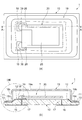
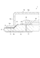
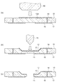
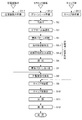
図1は、電子装置としての圧電デバイスの一実施形態を説明するものであり、(a)は上側からみた概略平面図、(b)は(a)のA−A線断面を示す概略断面図である。なお、図1(a)では、圧電デバイスの内部の構造を説明する便宜上、圧電デバイスの上方に設けられるキャップ体(19)の一部を切り欠いて図示している。また、図2は、図1(b)のD部を拡大して詳しく説明する部分断面図である。
(Piezoelectric device)
1A and 1B are diagrams for explaining an embodiment of a piezoelectric device as an electronic apparatus, wherein FIG. 1A is a schematic plan view seen from above, and FIG. 1B is a schematic cross-sectional view showing a cross section taken along line AA in FIG. It is. In FIG. 1A, for convenience of explanation of the internal structure of the piezoelectric device, a part of the cap body (19) provided above the piezoelectric device is cut out. FIG. 2 is a partial cross-sectional view illustrating the D portion of FIG.
図1において、圧電デバイス1は、基板としてのセラミック基板10と、そのセラミック基板10上に接合された電子部品としての圧電振動片20と、圧電振動片20を覆うようにセラミック基板10上に接合された凹状のキャップ体19と、を有し、セラミック基板10とキャップ体19とにより形成されるキャビティーT内に圧電振動片20が気密封止されている。
In FIG. 1, a
セラミック基板10は、平板状の絶縁性基材の一方の主面に複数の外部実装端子16を有し、他方の主面に圧電振動片20が接合される振動片接合端子18を有している。振動片接合端子18、および、図示しないその他の端子は、セラミック基板10に設けた貫通孔(ビアホール)に高融点金属を含む導体ペーストを埋設することにより形成された層内配線(ビア)17により対応する外部実装端子16に接続されている。
外部実装端子16が設けられたセラミック基板10の一方の主面は圧電デバイス1の外底面となり、その外底面に設けられた外部実装端子16によって、圧電デバイス1を電子機器などの外部実装基板に実装することができる。本実施形態のセラミック基板10はセラミック基板用のグリーンシートを成形・加工してから焼成することにより形成されている(詳細について後述する)。
The
One main surface of the
セラミック基板10の振動片接合端子18が設けられた電子部品接合領域としての振動片接合領域側の面(他方の主面)の周縁部には、その振動片接合領域の面と平行に、且つ、振動片接合領域を囲むように環状の段部11が形成されている。段部11と振動片接合領域とによる段差の壁面12は、段部11側から振動片接合領域の面側に傾斜して設けられている。
また、段部11上と壁面12上には、振動片接合領域を囲むように環状の金属層13が設けられている。
The peripheral part of the surface (the other main surface) on the side of the resonator element bonding region as the electronic component bonding region provided with the resonator
An
圧電振動片20は、例えば、水晶などの圧電体材料により形成された平板状の圧電基板の両主面に、対向電極としての励振電極25が設けられている。また、圧電振動片20の各主面の一端部側には外部接続電極26が設けられ、各々が対応する励振電極25から引き出された電極間配線により電気的に接続されている。なお、圧電振動片20の材質として、水晶以外の圧電体材料では、例えばタンタル酸リチウム、ニオブ酸リチウムなどが挙げられ、また、圧電体材料以外では、シリコンなどを挙げることができる。
In the piezoelectric vibrating
セラミック基板10上(他方の主面側)において、圧電振動片20は、その一端側に設けられた外部接続電極26をセラミック基板10の対応する振動片接合端子18と位置合わせした状態で、例えば銀ペーストなどの接合部材39により電気的な接続をはかりながら接合され、他端部側を自由端として片持ち支持されている。
On the ceramic substrate 10 (the other main surface side), the piezoelectric vibrating
凹状のキャップ体19は、例えば42アロイやコバール、あるいはリン青銅などの金属からなる板材を従来周知の板金加工により成形してなり、中央部に凹部が形成され、外周部には段部11と全周に渡って対面可能な鍔状の当接脚部19cが環状に形成されている。すなわち、キャップ体19は、中央部に水平部19aを有し、その水平部19aの外周側で一旦鉛直方向に曲げられて側壁部19bが形成され、さらにその側壁部19bから外周側に垂直に曲げられることにより、キャップ体19の外周部に水平部19aと略平行な環状の当接脚部19cが形成されている。
The
このキャップ体19は、水平部19aと側壁部19bとにより形成される凹部の開口部側をセラミック基板10側に向けた状態で、当接脚部19cをセラミック基板10の段部11に対向させて接合されている。本実施形態では、図2に示すように、セラミック基板10の段部11および壁面12上の金属層13と、キャップ体19の当接脚部19cの下面側およびその側面の内側(凹部側)の当接脚部19c寄りとが、例えば、比較的低融点の合金からなる接合部材としてのろう材29を介して接合されている。キャップ体19は、その凹部とセラミック基板10の圧電振動片20接合面とで囲まれたキャビティーT内に圧電振動片20を収容させることによって圧電振動片20の搭載領域を気密封止するためのものである。
The
ここで、本実施形態の圧電デバイス1では、上述したように、セラミック基板10の振動片接合領域側の面の周縁部に、振動片接合領域の面側に傾斜して設けられた壁面12と連結した段部11が形成されている。これにより、壁面12と圧電振動片20接合面とにより形成される凸部に、その壁面12をガイドにしてキャップ体19を嵌め込むようにして容易に位置決めすることができるので、キャップ体19の開口形状に製造ばらつきがあった場合でも、キャップ体19の位置ずれを防止して、例えば、圧電デバイス1の外周からキャップ体が突出して平面外形の寸法規格を満足せずに外観不良となったり、キャップ体19の接合強度や封止気密度が低下したりする不具合を回避することができる。
また、周縁部に段部11が設けられたセラミック基板10を用いた本実施形態の圧電デバイス1によれば、従来のセラミック基板のように平坦な面上にキャップ体を接合した場合に比して、キャップ体19の当接脚部19cとセラミック基板10の段部11との接合だけでなく、壁面12の段部11との境界部近傍と側壁部19bとの接合もされるので、セラミック基板10へのキャップ体19の接合強度が向上し、圧電振動片20を確実に気密封止することができるようになっている。
Here, in the
Moreover, according to the
また、キャップ体19は、段部11および壁面12に設けられた金属層13を介してセラミック基板10の図示しないグランド端子に電気的に接続されることが好ましい。このようにすれば、圧電デバイス1の使用時に、金属からなるキャップ体19がグランド電位に保持されることにより、圧電振動片20をキャップ体19のシールド効果によって外部からの不要な電気的作用、例えばノイズなどから保護することができる。
The
かくして上述した圧電デバイス1は、セラミック基板10の底面に設けられた外部実装端子16を介して圧電振動片20の両主面に設けられた励振電極25間に外部からの変動電圧を印加し、圧電振動片20の特性に応じた所定の周波数で振動を起こさせることによって圧電デバイス1として機能し、かかる圧電デバイス1の共振周波数に基づいて外部の発振回路で所定周波数の基準信号を発振・出力することができる。そして、このような基準信号は、例えば携帯用通信機器などの電子機器におけるクロック信号として利用することができる。
Thus, the
(圧電デバイスの製造方法)
次に、上記構成の圧電デバイス1の製造方法について、特に、セラミック基板10の製造方法を中心として図面に沿って説明する。
図3は、圧電デバイス1の製造方法の一実施形態を説明するフローチャートである。
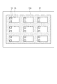
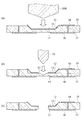
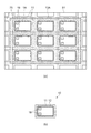
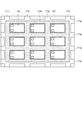
また、図4〜図9は、グリーンシートにより多数のセラミック基板を一括製造する過程を模式的に示すものであり、図4、図5、および図8は概略平面図、図6、図7、および図9は、図2と同じ断面を拡大して説明する部分断面図である。
(Piezoelectric device manufacturing method)
Next, a method for manufacturing the
FIG. 3 is a flowchart for explaining an embodiment of a method for manufacturing the
FIGS. 4 to 9 schematically show a process of collectively manufacturing a large number of ceramic substrates using a green sheet. FIGS. 4, 5, and 8 are schematic plan views, FIGS. FIG. 9 is a partial cross-sectional view illustrating the same cross section as FIG. 2 in an enlarged manner.
圧電デバイス1の製造工程は、圧電振動片20、セラミック基板10、およびキャップ体19をそれぞれ準備する前工程と、セラミック基板10上に圧電振動片20を接合してからキャップ体19を接合して圧電振動片20を気密封止する後工程(組立工程)とに大別することができる。まず、前工程のうち、圧電振動片20、およびキャップ体19の準備について概略を説明する。
The manufacturing process of the
ステップS1−1に示す圧電振動片20準備では、圧電振動片20を製造して圧電デバイス1組立ができる形態にする。圧電振動片20は、例えば水晶などの圧電体材料を所定のサイズに切り出して研磨した大判のウェハーに複数並べて一括形成することができる。概要を説明すると、まず、結晶軸に対して所定のカット角で切り出してから所望の厚さおよび表面状態となるように研磨加工した大判の水晶基板(水晶ウェハー)を準備する。そして、フォトリソグラフィを用いたウェットエッチングにより、水晶基板に複数の圧電振動片20の外形を形成する。なお、圧電振動片20の外形は、水晶基板から完全に切り離されないようにミシン目状の折り取り部などにより水晶ウェハーにつなげたまま、以降の工程を水晶基板(ウェハー)状態にて効率的に流動することが好ましい。そして、スパッタリングや蒸着などによって、励振電極25や外部接続電極26などの電極形成を行うことにより、水晶ウェハーに複数の圧電振動片20がマトリクス状に形成される。
In the preparation of the piezoelectric vibrating
ステップS1−3に示すキャップ体19準備では、キャップ体19を製造して圧電デバイス1組立ができる形態にする。キャップ体19は、例えば、42アロイやコバール、あるいはリン青銅などの金属からなる板材を、従来周知の板金加工により成形することによって、中央部に凹部が形成され、外周部に当接脚部19cが環状に設けられたキャップ体19を形成する。
In the preparation of the
次に、セラミック基板10の製造から圧電デバイス1組立までの製造工程を続けて説明する。
本実施形態では、セラミック基板10の基材としてセラミックのグリーンシートが用いられており、セラミック基板10の製造では、まず、ステップS1−2に示すように、複数のセラミック基板10をマトリクス状、すなわち、m列×n行(n,mは2以上の自然数)の行列状に並べて形成できるサイズのグリーンシート51(図4を参照)の準備をする。なお、図4,5,8,11,12に示すグリーンシート51において、1つのセラミック基板10の形成領域は圧電デバイス形成領域1Aとして図示している。グリーンシート51は、一般に、セラミック粉末を含むスラリーをドクターブレード法によりフィルム上に均一に載せ、そのスラリーを乾燥させてから所望の大きさの矩形状に切断することによって得ることができる。なお、セラミック粉末の材料は特に限定されるものではないが、耐熱性、耐絶縁性、耐磨耗性、耐気密性などの特性や、電気的特性に優れるアルミナ(Al2O3)やアルミナイトライド(AlN=窒化アルミニウム)などを用いることができる。また、スラリーには、セラミック粉末の他に有機バインダー、可塑剤、及び溶剤などが添加され、グリーンシート51が未焼成のこの段階では、グリーンシート51は比較的高い可塑性を有している。
Next, the manufacturing process from manufacturing the
In the present embodiment, a ceramic green sheet is used as the base material of the
次に、ステップS2に示すように、各圧電デバイス形成領域1Aにおいて、セラミック基板10の両主面の導通を図るために必要となる通電用の層内配線を形成するための貫通孔(ビアホール)を、例えばプレス加工やパンチング加工などにより形成する孔あけを行う。
次に、ステップS3に示すように、セラミック基板10にあけた貫通孔に、例えばタングステン(W)やモリブデン(Mo)などの高融点金属を含む導体ペーストをスクリーン印刷などの方法により充填することによってビアホール導通化を図り、セラミック基板10の両主面間を電気的に接続する層内配線17を形成する。
次に、ステップS4に示すように、例えばタングステンやモリブデンなどの高融点金属を含む導体ペーストをスクリーン印刷することにより、振動片接合端子18や金属層13、あるいは端子間配線やめっき用導体パターンなどの下地となる導体パターンを形成する。めっき用導体パターンは、後述するステップS7の導体パターンめっきステップにて、振動片接合端子18や金属層13に必要な金属めっき皮膜を電解めっきにより形成する際に、端子間配線を介してめっき電圧を供給するためのめっき用配線を指す。なお、図4は、グリーンシート51の複数の圧電デバイス形成領域1Aに振動片接合端子18の下地となる導体パターンが印刷され、さらに、金属層13の原形となる導体パターン13Aが形成された状態を示している(端子間配線やビアホールおよびめっき用導体パターンなどは図示を省略)。
なお、ステップS3のビアホール導通化とステップS4の導体パターン印刷は、スクリーン印刷により同時に行うことも可能である。
Next, as shown in step S2, in each piezoelectric
Next, as shown in step S3, a conductive paste containing a refractory metal such as tungsten (W) or molybdenum (Mo) is filled in the through holes formed in the
Next, as shown in step S4, for example, a conductive paste containing a refractory metal such as tungsten or molybdenum is screen-printed, so that the resonator
The via hole conduction in step S3 and the conductor pattern printing in step S4 can be simultaneously performed by screen printing.
次に、ステップS5に示すように、グリーンシート51から個片の圧電デバイス1に分割する際に折り取り可能となるように設ける分割溝と、段部11とを、押圧刃で押圧して設ける(図5および図6(a),(b)を参照、ただし、分割溝は図示を省略)。なお、図示を省略した分割溝は、段部11よりも幅狭な押圧刃を使用して、段部11よりも強く押圧することにより凹部の深い分割溝を形成する。分割溝の大きさおよび深さは、通常のハンドリングなどでは折れない程度で、且つ、無理なく折り取り作業をすることが可能な形状とする(ただし、本実施形態では、分割溝に沿って折り取ることにより圧電デバイスを個片化する方法ではなく、個々の圧電デバイスに加わるダメージを軽減するためにダイシングを用いて個片化する方法について後述する)。
Next, as shown in step S5, the dividing groove provided so that it can be folded when the
以下、分割溝および段部11を形成するステップにおける段部11の形成について説明する。
段部11の形成では、図6(a)に示すように、グリーンシート51と最初に当接される面に対して垂直な所定の傾斜で外側に広がる両側面を有する押圧刃60を、所定の圧力でグリーンシート51を押圧する。すると、図6(b)に示すように、可塑性を有する未焼成のグリーンシート51の塑性変形により押圧刃60の形状の凹部が形成される。すなわち、グリーンシート51の振動片接合端子18が設けられた振動片接合領域の面と平行な段部11と、その段部11から振動片接合領域の面に向かって傾斜する壁面12とが形成される。
このように、振動片接合領域の面側に傾斜した壁面12を有する段部11の形成は、従来のセラミック基板の製造工程に含まれるプレス加工による分割溝形成ステップにおいて、段部11形成用の押圧刃60を用いることのみにより、新たな工程や設備を増設することなく行うことができる。
Hereinafter, the formation of the
In the formation of the
As described above, the formation of the
次に、ステップS6に示すように、壁面12を有する段部11が形成されたグリーンシート51を還元雰囲気中の高温で焼成してセラミックシートを形成する。例えば、グリーンシート51のセラミック粉末がアルミナの場合には1550℃程度の高温で上記導体パターンの高融点金属と同時焼成する。なお、以降のステップS7から完成までのステップの説明のなかで記載したグリーンシート51とは、焼成したグリーンシート51であって、すなわちセラミックシートのことを指す。
次に、ステップS7に示すように、焼成したグリーンシート51を電解めっき液中に浸漬し、上記しためっき用導体パターンを介して通電を行い、振動片接合端子18や金属層13などの露出する高融点金属からなる全ての導体パターンに電解めっき皮膜(図示せず)を形成する。この電解めっき皮膜は、特に種類を限定するものではないが、例えば、電解ニッケル皮膜や電解金皮膜、あるいはニッケルと金とをこの順に積層させた複数層の電解めっき皮膜などがある。
以上、ステップS1−2のグリーンシート51準備からステップS2〜ステップS7までのステップにより、段部11を有するセラミック基板10がマトリクス状に複数形成されたグリーンシート51が完成する(図5を参照)。
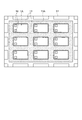
なお、この段階で、グリーンシート51から個片のセラミック基板10に分割することもできる。例えば、図8(a)に示すように、複数の圧電デバイス形成領域1Aがマトリクス状に形成されたグリーンシート51を、図中、想像線(二点鎖線)で示すダイシングライン75に沿ってダイシングすることなどにより、図8(b)に示す個片のセラミック基板10を得ることができる。
本実施形態では、複数のセラミック基板10が一体に形成されたグリーンシート51の状態のままで、圧電デバイス1の組立を効率的に行う方法について、以下、説明する。
Next, as shown in step S6, the
Next, as shown in step S <b> 7, the fired
As described above, the
At this stage, the
In the present embodiment, a method for efficiently assembling the
圧電デバイス組立工程では、まず、ステップS8に示すように、グリーンシート51の各圧電デバイス形成領域1Aに、上記ステップS1−1で準備した圧電振動片20を接合する。具体的には、各圧電デバイス形成領域1Aの振動片接合端子18上に、ディスペンサーやスクリーン印刷などにより銀ペーストなどの接合部材39を塗布してから、圧電振動片20の一端側に設けられた外部接続電極26を、対応する振動片接合端子18に位置合わせして仮止めする。そして、接合部材39の硬化方法に応じた処理、例えば、熱硬化型の接合部材39であれば所定の温度で加熱し、また、紫外線硬化型の接合部材であれば紫外線を照射することにより接合部材39を固化させて、圧電振動片20を片持ち支持された態様に接合する。
In the piezoelectric device assembly process, first, as shown in step S8, the piezoelectric vibrating
次に、ステップS9に示すように、圧電振動片20が接合されたグリーンシート51の各圧電デバイス形成領域1Aにキャップ体19を配置する。この工程では、キャップ体19を、上述した段部11形成ステップによりグリーンシート51の各圧電デバイス形成領域1Aに形成された壁面12と振動片接合領域の面とによる凸部にキャップ体19を嵌め込むようにすることにより容易に位置合わせして配置することができる。なお、このとき、段部11および壁面12の表面の金属層13とキャップ体19の側壁部19bおよび当接脚部19cとの間にはろう材29を介在させる。
ろう材29としては、金−ニッケル(Au−Ni)や金−錫(Au−Sn)あるいは金−ゲルマニウム(Au−Ge)などの合金(共晶合金)や半田などのろう材を用いることができる。また、低融点ガラスや、封止材として用いられる接着剤などを利用することもできる。なお、ろう材29は、セラミック基板10の金属層13上や、キャップ体19のセラミック基板10との当接部分にその一部を設けておく構成としてもよい。
Next, as shown in step S <b> 9, the
As the
次に、ステップS10に示すように、キャップ体19とセラミック基板10の段部11および壁面12(金属層13)とがろう材29を介して当接された状態のグリーンシート51を、例えば、300℃〜350℃の温度に保持された恒温炉内に入れて、ろう材29を加熱・溶融させることによりキャップ体19をセラミック基板10に接合する。本実施形態では、金属からなるキャップ体19を、金属系のろう材をろう材29として接合することにより、キャップ体19による圧電振動片20の気密封止をより強固で確実なものとすることができる。
Next, as shown in step S10, the
なお、上述した一連のセラミック基板10へのキャップ体19接合ステップ(ステップS9のキャップ体19配置、および、ステップS10のキャップ体19接合)は、例えば、窒素ガスやアルゴンガスなどの不活性ガス雰囲気、あるいは減圧空間内で行うことが好ましい。これによって、圧電振動片20が収納されるセラミック基板10とキャップ体19とにより形成されるキャビティーTの内部が不活性ガスが充満され、あるいは減圧空間に密閉・封止されるので、圧電振動片20が酸素や大気中の水分などによって腐食・劣化するのを有効に防止することができる。
以上、説明した一連のステップを経て、グリーンシート51に、複数の圧電デバイス1がマトリクス状に形成される。
In addition, the above-described series of
As described above, the plurality of
次に、ステップS11に示すように、上述したステップS10までのステップを経たグリーンシート51を分割して複数の個片の圧電デバイス1を同時に得る。グリーンシート51の分割は、例えば図8に示すダイシングライン75に沿って、図6(b)に示すダイシングソーの高速回転するダイシングブレード70によってダイシングすることなどにより、図6(c)に示すように切断することができる。
Next, as shown in step S11, the
ただし、図6に示すように、グリーンシート51に形成された金属層13がダイシングライン75にかかっている場合には、金属層13を切断する際とグリーンシート51のセラミック基材を切断する場合とでダイシングブレード70を交換しないと、切断面にバリやカエリなどの形状品質異常が生じたり、ダイシングブレード70の劣化が早く進行したりして製造効率を低下させる虞がある。
このような不具合を回避する方法として、上記ステップS5の分割溝・段部形成ステップで分割溝および段部11を形成した後で、図7(a)に示すように、角錐状の断面を有する押圧刃60Bを用いて段部11のダイシングライン上に圧痕52を形成する。このとき、圧痕52の幅はダイシングブレード70の幅と同じか若干広くすることが好ましい。これにより、圧痕52を形成した部分の金属層はさらに圧延されて極薄くなるので、グリーンシート51の基材をダイシングするのに適したダイシングブレード70を用いてダイシングすることにより、図7(c)に示すように良好な切断面にて複数の圧電デバイス1が形成されたグリーンシート51の分割をすることができる。
また、さらに良好なダイシングを行なう方法として、上記ステップS4の導体パターン印刷ステップで、図9(a)に示すように、グリーンシート51のダイシングラインとなる領域を避けて金属層13の原形となる導体パターン13Bを形成する。このようにすれば、図9(b)に示すようにグリーンシート51の基材をダイシングするのに適したダイシングブレード80を用いてダイシングすることにより、図9(c)に示すようにさらに良好な切断面にて圧電デバイス(1)のグリーンシート51からの分割をすることができる。
However, as shown in FIG. 6, when the
As a method for avoiding such a problem, as shown in FIG. 7A, after forming the dividing groove and
Further, as a method for performing better dicing, in the conductor pattern printing step of step S4, as shown in FIG. 9A, the original shape of the
分割ステップにより得られた圧電デバイス1は、ステップS12に示すように、電気的特性や外観品質の検査を行なうことにより完成され、一連の圧電デバイス1の製造工程を終了する。
The
上記実施形態の圧電デバイス1の製造方法によれば、セラミック基板10の振動片接合領域側の面の周縁部に、振動片接合領域の面側に傾斜して設けられた壁面12と連結した段部11が形成されている。これにより、壁面12と圧電振動片20接合面とにより形成される凸部に、その壁面12をガイドにしてキャップ体19を嵌め込むようにして容易に位置決めすることができるので、キャップ体19の開口形状に製造ばらつきがあった場合でも、キャップ体19の位置ずれを防止して、例えば、圧電デバイス1の外周からキャップ体が突出して平面外形の寸法規格を満足せずに外観不良となったり、キャップ体19の接合強度や封止気密度が低下したりする不具合を回避することができる。
また、周縁部に段部11が設けられたセラミック基板10を用いた本実施形態の圧電デバイス1によれば、従来のセラミック基板のように平坦な面上にキャップ体を接合した場合に比して、キャップ体19の当接脚部19cとセラミック基板10の段部11との接合だけでなく、壁面12の段部11との境界部近傍と側壁部19bとの接合もされるので、セラミック基板10へのキャップ体19の接合強度が向上し、圧電振動片20を確実に気密封止することができる。
According to the method for manufacturing the
Moreover, according to the
また、上記実施形態では、セラミック基板の材料として可塑性を有する未焼成のグリーンシート51を利用し、そのグリーンシートを用いたセラミック基板の製造工程において標準的なステップである押圧刃60による分割溝形成ステップにて、段部11を形成してから焼成を行う工順とした。
これにより、既存の設備を利用して、また、従来の製造工程からの増大を抑えながら、比較的容易に段部11および段部11の壁面12を形成することができる。
Moreover, in the said embodiment, the division | segmentation groove | channel formation by the
Thereby, it is possible to form the
上記実施形態で説明した圧電デバイスおよびその製造方法は、以下の変形例として実施することも可能である。 The piezoelectric device and the manufacturing method thereof described in the above embodiment can be implemented as the following modifications.
(変形例1)
上記実施形態の圧電デバイス1の製造方法では、グリーンシート51の複数の圧電デバイス形成領域1Aに対して、平面視でコーナー部が丸められた矩形状の段部11(図5を参照)を、押圧刃60により一括により形成(図5,図6を参照)する方法を説明した。これに限らず、複数種類の押圧刃を用意して段部11の形状を複数回に分けて形成する構成としてもよい。
図10は、段部の形状を複数回に分けて形成する圧電デバイスの製造方法の変形例を説明するフローチャートである。また、図11および図12は、グリーンシートに、複数種類の押圧刃を用いて複数回に分けて段部を形成する過程を説明する概略平面図である。なお、段部が完成した状態のグリーンシートの図は、上記実施形態の説明で用いた図5を参照する。また、図10に示すフローチャートや、図11および図12に示すグリーンシートにおいて、上記実施形態と同じ構成については同一符号を付して説明を省略する。
(Modification 1)
In the manufacturing method of the
FIG. 10 is a flowchart for explaining a modified example of the method for manufacturing a piezoelectric device in which the shape of the step portion is formed in a plurality of times. FIG. 11 and FIG. 12 are schematic plan views for explaining the process of forming a step portion in a plurality of times using a plurality of types of pressing blades on the green sheet. In addition, the figure of the green sheet in a state where the stepped portion is completed refers to FIG. 5 used in the description of the above embodiment. Further, in the flowchart shown in FIG. 10 and the green sheets shown in FIGS. 11 and 12, the same components as those in the above embodiment are denoted by the same reference numerals and description thereof is omitted.
本変形例の分割溝および段部形成ステップ(図3のステップS5)では、まず、図10のステップS5−1に示すように、角付きの段部を形成する。ここで、本変形例では、角付きの段部を、さらに二段階に分けて形成する方法を説明する。
すなわち、上記実施形態の圧電デバイス1の製造方法の導体パターン印刷ステップ(ステップS4)までのステップを経て、振動片接合端子18や金属層の原形となる導体パターン13Aなどが形成されたグリーンシート51(図4を参照)に、図11に示すように、まず、マトリクス状に配置された複数の圧電デバイス形成領域1Aの段部(11)の縦横いずれか一方の外形となる複数の段部11aを形成する。本変形例では、各圧電デバイス形成領域1Aの段部(11)の長手方向側の外形となる段部11aを最初に形成した例を示している。
なお、図11では、グリーンシート51に4列の段部11aを形成した例を図示しているが、これら4列の段部11aは、4列の段部11aを形成できる形状の押圧刃を用意して一括して押圧加工することにより形成することができる。この場合、加工時間をより短縮することができる。
また、4列の段部11aは、1列の段部11aを形成できる形状の押圧刃を用意して、4回に分けて押圧加工することにより形成することができる。また、2列の段部11aを形成できる押圧刃を用意して2回に分けて4列の段部11aを形成することもできる。このように、最終的に形成される段部11aの列数の約数の段部11aを形成可能な押圧刃により複数回に分けて段部11aを形成する方法を用いた場合には、押圧刃の汎用化が可能になり、また、1回の押圧加工の際に押圧刃に印加する圧力が低くて済むとともに、1つの段部11aごとに形成位置を調整することも可能なので、段部11aの位置精度や形状を安定化させ易い。
In the dividing groove and step forming step (step S5 in FIG. 3) of this modification, first, a stepped portion with a corner is formed as shown in step S5-1 in FIG. Here, in this modification, a method of forming the stepped portion with corners in two steps will be described.
That is, through the steps up to the conductor pattern printing step (step S4) of the manufacturing method of the
FIG. 11 shows an example in which four rows of
Further, the four rows of
次に、図12に示すように、複数の圧電デバイス形成領域1Aの段部(11)の縦横の外形のうち、上記の段部11aとは異なる他方の外形となる複数の段部11bを形成する。
なお、図12では、グリーンシート51に形成された4列の段部11bを形成した例を図示しているが、上記の段部11aの場合と同様に、4列の段部11bを、4列の段部11bを形成できる形状の押圧刃を用意して一括して押圧加工することにより形成することもでき、また、最終的に形成される段部11bの列数の約数の段部11bを形成可能な押圧刃により、複数回に分けて形成することもできる。
Next, as shown in FIG. 12, among the vertical and horizontal outer shapes of the step portion (11) of the plurality of piezoelectric
FIG. 12 shows an example in which four rows of
ここまでのステップにより、グリーンシート51に形成された各圧電デバイス形成領域1Aの段部(11)のうち、平面視でコーナー部が丸められていない矩形状の段部11a,11bには、次に、ステップS5−2に示すように、各コーナー部を平面視で丸めた形状に成形することが可能な押圧刃を用いて押圧加工することにより、図5に示すように、各圧電デバイス形成領域1Aにおけるコーナー部に丸みを有する段部11の形成を完了させる。
なお、このステップの押圧加工においても、コーナー部を丸めた形状に成形することが可能な形状の押圧刃は、グリーンシート51内の全てのコーナー部を一括して丸めた形状に押圧加工することにより形成してもよく、また、グリーンシート51内の一部のコーナー部を丸めた形状に成形することが可能な押圧刃により、複数回に分けて形成してもよい。
Of the steps (11) of each piezoelectric
Even in the pressing process of this step, the pressing blade having a shape that can be formed into a rounded corner portion is to press all the corner portions in the
上記変形例1の圧電デバイスの製造方法によれば、押圧刃を用いてプレス加工することにより段部11を形成する際に、複数回に分けて押圧加工することにより、1回の押圧加工の際に印加する圧力が低くて済むので、グリーンシート51に加わるダメージが軽減されるとともに、コーナー部ごとに形成位置を精緻に調整することが可能になり形状の安定化を図ることができる。
According to the method for manufacturing a piezoelectric device of the first modification, when the
(変形例2)
上記実施形態では、セラミック基板10の壁面12において、段部11から圧電振動片20接合面にまでに渡って金属層13を形成した。これに限らず、壁面の金属層を、圧電振動片20接合面から所定の隙間を設けて形成することにより、キャップ体接合時に発生する虞のある不具合を回避することが可能になる。
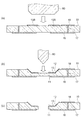
図13は、壁面の金属層の形成位置を規定した圧電デバイスの変形例2を示すものであり、図2と同じ断面を拡大して説明する部分断面図である。なお、図13に示す圧電デバイスの変形例2において、上記実施形態の圧電デバイス1と同じ構成については同一符号を付して説明を省略する。
(Modification 2)
In the above embodiment, the
FIG. 13 shows a second modification of the piezoelectric device in which the formation position of the metal layer on the wall surface is shown, and is a partial cross-sectional view illustrating the same cross-section as in FIG. In addition, in the modification 2 of the piezoelectric device shown in FIG. 13, the same code | symbol is attached | subjected about the same structure as the
図13において、本変形例の圧電デバイス101のセラミック基板10は、振動片接合端子18が設けられた圧電振動片20接合面の周縁部に、その振動片接合領域の面と平行に段部11が形成されている。段部11と振動片接合領域の面とを接続する壁面112は、段部11から振動片接合領域の面側に傾斜して設けられている。
また、段部11の面上と壁面112上には金属層13が設けられている。このうち、壁面112の金属層13は、振動片接合領域の面から隙間を空けて設けられている。
In FIG. 13, the
A
上記変形例2の構成によれば、壁面112の圧電振動片20接合面側に金属層13が無いので、圧電振動片20が接合されたセラミック基板10にろう付けによりキャップ体19を接合する際に、金属や合金からなるろう材29(ろう材)の溶融飛沫が圧電振動片20の励振電極25などに飛散することにより発生し得る圧電振動片20の振動特性の低下を抑えることができる。
According to the configuration of the second modification, since the
(変形例3)
上記実施形態および変形例1,2では、セラミック基板10の段部11と傾斜を有する壁面12,112との接続部分の断面形状が角部となっている形態について説明した。これに限らず、段部から壁面にかけての形状を、キャップ体の側壁部から当接脚部にかけての形状に合わせて丸みを帯びた形状とすることにより、圧電デバイスの機械的な強度、あるいは、セラミック基板へのキャップ体の接合強度の向上を図ることができる。
図14は、段部から壁面にかけての形状を変更した圧電デバイスの変形例3を示すものであり、図2(および図13)と同じ断面を拡大して説明する部分断面図である。なお、図14に示す圧電デバイスの変形例3において、上記実施形態の圧電デバイス1と同じ構成については同一符号を付して説明を省略する。
(Modification 3)
In the above-described embodiment and the first and second modifications, the embodiment in which the cross-sectional shape of the connection portion between the
FIG. 14 shows a third modification of the piezoelectric device in which the shape from the step portion to the wall surface is changed, and is a partial sectional view illustrating the same section as FIG. 2 (and FIG. 13) in an enlarged manner. In addition, in the modification 3 of the piezoelectric device shown in FIG. 14, the same components as those of the
図14において、本変形例の圧電デバイス1´のセラミック基板10は、振動片接合端子18が設けられた圧電振動片20接合面の周縁部に、その振動片接合領域の面と平行に段部11´が形成されている。段部11´と振動片接合領域の面とを接続する壁面12´は、段部11´から振動片接合領域の面側に傾斜して設けられている。
また、段部11´と壁面12´との接続部分111は、角張らずに丸みを帯びた断面形状を呈している。この接続部分111の丸みを帯びた断面形状は、段部11´と壁面12´とに当接させて接合されるキャップ体19の側壁部19bと当接脚部19cとの接続部と略同じ丸みにて形成されていることが望ましい。また、この丸みを帯びた接続部分111の形状は、段部11´を形成するステップ(図3のステップS5に示す分割溝・段部形成ステップ)で、丸みを帯びた接続部分111により接続された段部11´と壁面12´とを形成できる形状の押圧刃を用意して、その押圧刃により押圧加工することにより形成することができる。
In FIG. 14, the
Further, the connecting
上記実施形態のように、電子部品(圧電振動片20)を接合した基板(セラミック基板10)を、キャップ体19により気密封止する構造の電子装置(圧電デバイス1)では、キャップ体19は金属材料を周知の板金加工により形成することが多く、その場合、キャップ体19の側壁部19bと当接脚部19cとを垂直に接続する接続部分は丸みを帯びた断面形状にて曲げ加工される。
上記変形例3の圧電デバイス1´によれば、段部11´と壁面12´とを接続する接続部分111の断面形状が、キャップ体19の側壁部19bと当接脚部19cとを接続する丸みを帯びた断面形状の接続部分と近似な断面形状を有して形成されている。これにより、セラミック基板10の厚みが薄くなる基点となる段部11´と壁面12´との接続部分に応力が生じた場合に起こり得るクラックなど発生を抑えることができるので、圧電デバイス1´の機械的な強度の向上を図ることができる。
また、キャップ体19とセラミック基板10との接合において互いに当接される部分、または、近接する部分が大きくなることにより、良好な接合状態が得られやすく、高い気密度にて封止された動作安定性の高い圧電デバイス1´を提供することができる。
In the electronic device (piezoelectric device 1) having a structure in which the substrate (ceramic substrate 10) to which the electronic component (piezoelectric vibrating piece 20) is bonded is hermetically sealed by the
According to the
In addition, a portion that contacts or close to each other in the bonding of the
以上、発明者によってなされた本発明の実施の形態について具体的に説明したが、本発明は上記した実施の形態およびその変形例に限定されるものではなく、その要旨を逸脱しない範囲で種々の変更を加えることが可能である。 Although the embodiments of the present invention made by the inventor have been specifically described above, the present invention is not limited to the above-described embodiments and modifications thereof, and various modifications can be made without departing from the spirit of the present invention. It is possible to make changes.
例えば、上記実施形態および変形例では、基板としてのセラミック基板10が単層のグリーンシート51により形成された例を説明した。
これに限らず、グリーンシートからセラミック基板を製造する場合には、上記実施形態で説明した導電パターンが形成されたグリーンシート51を複数層積層させて形成する多層基板とすることもできる。
この場合、上記実施形態で説明した図3のステップS1−2のグリーンシート準備、および、ステップS2の孔あけから、ステップS4の導体パターン印刷までを経たグリーンシートを複数用意し、これら複数のグリーンシートを積層させて仮固定したのち、ステップS5の分割溝・段部形成を行ってからステップS6の焼成を行うことにより、段部を有する多層のセラミック基板を得ることができる。
For example, in the embodiment and the modification described above, an example in which the
However, the present invention is not limited thereto, and when a ceramic substrate is manufactured from a green sheet, a multilayer substrate formed by laminating a plurality of
In this case, a plurality of green sheets prepared from the green sheet preparation in step S1-2 in FIG. 3 described in the above embodiment and the drilling in step S2 to the conductor pattern printing in step S4 are prepared. After the sheets are stacked and temporarily fixed, the multi-layer ceramic substrate having the stepped portion can be obtained by performing the dividing groove / stepped portion formation in step S5 and then firing in step S6.
また、上記実施形態および変形例では、金属製のキャップ体19を用いて、また、セラミック基板10の段部11,11´および壁面12,12´,112に金属層13,13´を設けて、キャップ体19とセラミック基板10とを金属や合金からなるろう材29により接合する例を説明した。そのろう材による接合(ろう付け)は、母材(キャップ体19および金属層13,13´)よりも融点の低い金属や合金などからなるろう材29を接合部材として用いて、そのろう材29を溶融させて接合する方法を指し、例えば、接合前にキャップ体19とセラミック基板10との当接部分の間にろう材29を供給しておき、それを溶融させる方法の他に、キャップ体19およびセラミック基板10の両方またはいずれか一方に、ろう材29となる金属や合金の層を形成しておく方法なども含む。
また、本発明では、キャップ体19とセラミック基板10との接合に用いる接合部材は、上記実施形態および変形例のような金属や合金からなる接合部材に限らず、例えば、低融点ガラスや有機系(樹脂系)の接着剤を接合部材として接合する構成も含む。この場合、キャップ体19は金属製である必要はなく、また、段部11,11´および壁面12,12´に金属層13,13´を設ける必要がない。
Moreover, in the said embodiment and modification, the metal layers 13 and 13 'are provided in the
Further, in the present invention, the joining member used for joining the
また、上記実施形態および変形例で説明した特定の形態、例えば、セラミック基板10やグリーンシート51、あるいは電子部品としての圧電振動片20などの形状は限定されるものではない。
同様に、各電極、配線、端子などの位置や形状についても上記実施形態およびに限定されない。
In addition, the specific forms described in the above-described embodiments and modifications, for example, the shape of the
Similarly, the position and shape of each electrode, wiring, terminal, etc. are not limited to the above embodiment.
また、上記実施形態および変形例では、電子装置の一例として、電子部品としての圧電振動片20を搭載した圧電デバイス1,1´,101について説明した。これに限らず、上記実施形態および変形例に示す構成は、電子部品として半導体回路素子など種々の電子部品を基板に接合し、その電子部品をキャップ体により気密封止する構造の様々な電子装置に適用することができる。
In the embodiment and the modification, the
1…電子装置としての圧電デバイス、1A…圧電デバイス形成領域、10…基板としてのセラミック基板、11,11´…段部、11a…(段部の一部となるグリーンシートの)段部、12,12´,112…壁面、13…金属層、13A,13B…(金属層の原形となる)導体パターン、16…外部実装端子、18…振動片接合端子、19…キャップ体、19a…水平部、19b…側壁部、19c…当接脚部、20…電子部品としての圧電振動片、25…励振電極、26…外部接続電極、29…接合部材としてのろう材、39…接合部材、51…基板シートとしてのグリーンシート、52…圧痕、60,60B…押圧刃、70,80…ダイシングブレード、75…ダイシングライン、111…接続部分。
DESCRIPTION OF
Claims (8)
前記電子部品接合領域に接合されている電子部品と、
凹部と、前記凹部の外周部に設けられ前記段部に対面した鍔状の当接脚部と、を有し、前記電子部品を覆い、かつ前記段部に接合されているキャップ体と、を備え、
前記凹部の内周面と前記当接脚部の前記段部側の面との境界部が、前記基板の平面視にて、前記壁面内に位置していることを特徴とする電子装置。 An electronic component bonding region, a step portion around the electronic component bonding region, and a surface that is between the electronic component bonding region and the step portion and is inclined from the step portion side to the electronic component bonding region side. A substrate with walls,
An electronic component joined to the electronic component joining region;
A cap body that has a concave portion and a hook-shaped contact leg portion that is provided on an outer peripheral portion of the concave portion and faces the step portion, covers the electronic component, and is joined to the step portion. Prepared,
An electronic device , wherein a boundary portion between an inner peripheral surface of the concave portion and a surface of the contact leg portion on the stepped portion side is located in the wall surface in a plan view of the substrate .
前記壁面上の前記金属層と前記境界部が当接し、 The metal layer on the wall and the boundary abut,
前記金属層と前記境界部との当接部より外側では、前記段部上の前記金属層と前記当接脚部とがろう材を介して接合され、前記当接部より内側では、前記壁面上の前記金属層と前記凹部の内周面とがろう材を介して接合されていることを特徴とする請求項1または2に記載の電子装置。 Outside the contact portion between the metal layer and the boundary portion, the metal layer on the stepped portion and the contact leg portion are joined via a brazing material, and inside the contact portion, the wall surface 3. The electronic device according to claim 1, wherein the upper metal layer and the inner peripheral surface of the recess are joined via a brazing material.
前記電子部品接合領域に接合されている電子部品と、
凹部と、前記凹部の外周部に設けられ前記段部に対面した鍔状の当接脚部と、を有し、前記電子部品を覆い、かつ前記段部に接合されているキャップ体と、を備え、
前記凹部の内周面と前記当接脚部の前記段部側の面との境界部が、前記基板の平面視にて、前記壁面内に位置している電子装置の製造方法であって、
前記基板を形成可能な基板シートを準備するステップと、
プレス加工により前記基板シートから個片の前記基板に分割するための分割溝を形成する分割溝形成ステップと、
前記電子部品接合領域に前記電子部品を接合するステップと、
前記電子部品を覆うように前記基板に前記キャップ体を接合するステップと、
を含むことを特徴とする電子装置の製造方法。 An electronic component bonding region, a step portion around the electronic component bonding region, and a surface that is between the electronic component bonding region and the step portion and is inclined from the step portion side to the electronic component bonding region side. A substrate with walls,
An electronic component joined to the electronic component joining region;
A cap body that has a concave portion and a hook-shaped contact leg portion that is provided on an outer peripheral portion of the concave portion and faces the step portion, covers the electronic component, and is joined to the step portion. Prepared,
A method of manufacturing an electronic device , wherein a boundary between an inner peripheral surface of the recess and a surface of the contact leg on the stepped portion side is located in the wall surface in a plan view of the substrate ,
Providing a substrate sheet capable of forming the substrate;
A dividing groove forming step for forming a dividing groove for dividing the substrate sheet into the pieces of the substrate by pressing;
Bonding the electronic component to the electronic component bonding region;
Bonding the cap body to the substrate so as to cover the electronic component;
A method for manufacturing an electronic device, comprising:
前記セラミックシートを焼成する焼成ステップを含み、
前記焼成ステップの前に前記分割溝形成ステップを含むことを特徴とする請求項5に記載の電子装置の製造方法。 An unfired ceramic sheet is used as the material of the substrate sheet,
Including a firing step of firing the ceramic sheet;
6. The method for manufacturing an electronic device according to claim 5, further comprising the step of forming the dividing groove before the baking step.
前記分割溝形成ステップが、
平面視で矩形状の前記段部を形成するステップと、
前記段部の前記角部を曲線形状に加工するステップと、を含むことを特徴とする請求項5または6に記載の電子装置の製造方法。 The step has a rectangular shape with rounded corners in plan view,
The dividing groove forming step includes
Forming the rectangular stepped portion in plan view;
The method for manufacturing an electronic device according to claim 5, further comprising a step of processing the corner portion of the stepped portion into a curved shape.
前記基板シートに導体パターンを形成する導体パターン形成ステップを含み、
前記導体パターン形成ステップで、前記基板の前記壁面となる部分、および、前記段部となる部分の少なくとも前記段部または前記壁面の何れか一方との接続部分の近傍に前記導体パターンを形成することを特徴とする請求項5乃至7の何れか一項に記載の電子装置の製造方法。 The cap body has a metal or a metal layer at least in contact with the substrate;
Including a conductor pattern forming step of forming a conductor pattern on the substrate sheet,
In the conductor pattern forming step, the conductor pattern is formed in the vicinity of a portion that becomes the wall surface of the substrate and a connection portion between at least one of the step portion and the wall surface of the portion that becomes the step portion. The method for manufacturing an electronic device according to claim 5, wherein:
Priority Applications (3)
| Application Number | Priority Date | Filing Date | Title |
|---|---|---|---|
| JP2010016373A JP5407903B2 (en) | 2010-01-28 | 2010-01-28 | Electronic device and method of manufacturing electronic device |
| CN2010106234194A CN102185580A (en) | 2010-01-18 | 2010-12-28 | Electronic apparatus, method of manufacturing substrate, and method of manufacturing electronic apparatus |
| US12/984,929 US8941017B2 (en) | 2010-01-18 | 2011-01-05 | Electronic apparatus, method of manufacturing substrate, and method of manufacturing electronic apparatus |
Applications Claiming Priority (1)
| Application Number | Priority Date | Filing Date | Title |
|---|---|---|---|
| JP2010016373A JP5407903B2 (en) | 2010-01-28 | 2010-01-28 | Electronic device and method of manufacturing electronic device |
Publications (3)
| Publication Number | Publication Date |
|---|---|
| JP2011155172A JP2011155172A (en) | 2011-08-11 |
| JP2011155172A5 JP2011155172A5 (en) | 2013-03-14 |
| JP5407903B2 true JP5407903B2 (en) | 2014-02-05 |
Family
ID=44540921
Family Applications (1)
| Application Number | Title | Priority Date | Filing Date |
|---|---|---|---|
| JP2010016373A Expired - Fee Related JP5407903B2 (en) | 2010-01-18 | 2010-01-28 | Electronic device and method of manufacturing electronic device |
Country Status (1)
| Country | Link |
|---|---|
| JP (1) | JP5407903B2 (en) |
Families Citing this family (1)
| Publication number | Priority date | Publication date | Assignee | Title |
|---|---|---|---|---|
| JP5717869B2 (en) * | 2011-10-31 | 2015-05-13 | 京セラ株式会社 | Piezoelectric actuator |
Family Cites Families (10)
| Publication number | Priority date | Publication date | Assignee | Title |
|---|---|---|---|---|
| JP2637136B2 (en) * | 1988-02-12 | 1997-08-06 | 株式会社東芝 | Circuit board |
| JPS63208250A (en) * | 1987-02-25 | 1988-08-29 | Nec Corp | Package structure of integrated circuit |
| JP2895975B2 (en) * | 1991-03-13 | 1999-05-31 | 新光電気工業株式会社 | Ceramic package |
| JPH07221584A (en) * | 1994-02-09 | 1995-08-18 | Seikosha Co Ltd | Sealed container |
| JPH0964680A (en) * | 1995-08-25 | 1997-03-07 | Miyota Kk | Quartz oscillator and its production |
| JP3802225B2 (en) * | 1998-04-21 | 2006-07-26 | 日本電波工業株式会社 | Crystal oscillator |
| JP2001156193A (en) * | 1999-11-24 | 2001-06-08 | Kyocera Corp | Electronic component equipment |
| JP4369707B2 (en) * | 2003-08-28 | 2009-11-25 | 京セラ株式会社 | Piezoelectric vibrator |
| JP4699941B2 (en) * | 2006-05-17 | 2011-06-15 | 株式会社住友金属エレクトロデバイス | Ceramic package for electronic component storage |
| JP2011147054A (en) * | 2010-01-18 | 2011-07-28 | Seiko Epson Corp | Electronic apparatus, and method of manufacturing the same |
-
2010
- 2010-01-28 JP JP2010016373A patent/JP5407903B2/en not_active Expired - Fee Related
Also Published As
| Publication number | Publication date |
|---|---|
| JP2011155172A (en) | 2011-08-11 |
Similar Documents
| Publication | Publication Date | Title |
|---|---|---|
| US8941017B2 (en) | Electronic apparatus, method of manufacturing substrate, and method of manufacturing electronic apparatus | |
| JP2011147054A (en) | Electronic apparatus, and method of manufacturing the same | |
| CN1670978B (en) | Electronic device manufacturing method | |
| JP5312223B2 (en) | Wiring board | |
| JP7075810B2 (en) | Electronic component storage packages, electronic devices, and electronic modules | |
| JP5070973B2 (en) | Lid body assembly, piezoelectric vibration device using the lid body assembly, and method of manufacturing piezoelectric vibration device | |
| JP4859811B2 (en) | Electronic component storage package | |
| CN114762098B (en) | Electronic component storage package, electronic device and electronic module | |
| JP5407903B2 (en) | Electronic device and method of manufacturing electronic device | |
| JP5052470B2 (en) | Multi-cavity wiring board, wiring board and electronic device | |
| CN106229308B (en) | Ceramic package and its manufacturing method | |
| JP4439291B2 (en) | Piezoelectric vibrator storage package and piezoelectric device | |
| US11056635B2 (en) | Electronic component housing package, electronic device, and electronic module | |
| CN1734935A (en) | Ceramic package, assembled substrate, and manufacturing method therefor | |
| JP5725898B2 (en) | Electronic component storage package | |
| JP5252992B2 (en) | Crystal oscillator package and crystal oscillator | |
| JP4380419B2 (en) | Manufacturing method of electronic device | |
| JP4332037B2 (en) | Electronic component storage package and electronic device | |
| JP2013140876A (en) | Manufacturing method of electronic device, electronic device, piezoelectric oscillator, and electronic apparatus | |
| JP2004343072A (en) | Multi-cavity wiring board | |
| JP6129491B2 (en) | Multi-wiring board | |
| JP2005072421A (en) | Electronic component storage package and electronic device | |
| JP2013140874A (en) | Electronic device, ceramic substrate, manufacturing method, and piezoelectric oscillator | |
| JP2006332599A (en) | Electronic equipment | |
| JP2017022334A (en) | Multi-piece wiring board and manufacturing method thereof |
Legal Events
| Date | Code | Title | Description |
|---|---|---|---|
| A521 | Request for written amendment filed |
Free format text: JAPANESE INTERMEDIATE CODE: A523 Effective date: 20130124 |
|
| A621 | Written request for application examination |
Free format text: JAPANESE INTERMEDIATE CODE: A621 Effective date: 20130124 |
|
| A977 | Report on retrieval |
Free format text: JAPANESE INTERMEDIATE CODE: A971007 Effective date: 20130527 |
|
| A131 | Notification of reasons for refusal |
Free format text: JAPANESE INTERMEDIATE CODE: A131 Effective date: 20130604 |
|
| A521 | Request for written amendment filed |
Free format text: JAPANESE INTERMEDIATE CODE: A523 Effective date: 20130731 |
|
| RD03 | Notification of appointment of power of attorney |
Free format text: JAPANESE INTERMEDIATE CODE: A7423 Effective date: 20130731 |
|
| TRDD | Decision of grant or rejection written | ||
| A01 | Written decision to grant a patent or to grant a registration (utility model) |
Free format text: JAPANESE INTERMEDIATE CODE: A01 Effective date: 20131008 |
|
| A61 | First payment of annual fees (during grant procedure) |
Free format text: JAPANESE INTERMEDIATE CODE: A61 Effective date: 20131021 |
|
| R150 | Certificate of patent or registration of utility model |
Ref document number: 5407903 Country of ref document: JP Free format text: JAPANESE INTERMEDIATE CODE: R150 |
|
| S531 | Written request for registration of change of domicile |
Free format text: JAPANESE INTERMEDIATE CODE: R313531 |
|
| R350 | Written notification of registration of transfer |
Free format text: JAPANESE INTERMEDIATE CODE: R350 |
|
| LAPS | Cancellation because of no payment of annual fees |