JP2013140876A - Manufacturing method of electronic device, electronic device, piezoelectric oscillator, and electronic apparatus - Google Patents
Manufacturing method of electronic device, electronic device, piezoelectric oscillator, and electronic apparatus Download PDFInfo
- Publication number
- JP2013140876A JP2013140876A JP2012000502A JP2012000502A JP2013140876A JP 2013140876 A JP2013140876 A JP 2013140876A JP 2012000502 A JP2012000502 A JP 2012000502A JP 2012000502 A JP2012000502 A JP 2012000502A JP 2013140876 A JP2013140876 A JP 2013140876A
- Authority
- JP
- Japan
- Prior art keywords
- electronic device
- metal lid
- metallized layer
- ceramic substrate
- piezoelectric
- Prior art date
- Legal status (The legal status is an assumption and is not a legal conclusion. Google has not performed a legal analysis and makes no representation as to the accuracy of the status listed.)
- Withdrawn
Links
Images


Classifications
-
- H—ELECTRICITY
- H01—ELECTRIC ELEMENTS
- H01L—SEMICONDUCTOR DEVICES NOT COVERED BY CLASS H10
- H01L2924/00—Indexing scheme for arrangements or methods for connecting or disconnecting semiconductor or solid-state bodies as covered by H01L24/00
- H01L2924/15—Details of package parts other than the semiconductor or other solid state devices to be connected
- H01L2924/161—Cap
- H01L2924/1615—Shape
- H01L2924/16152—Cap comprising a cavity for hosting the device, e.g. U-shaped cap
-
- H—ELECTRICITY
- H01—ELECTRIC ELEMENTS
- H01L—SEMICONDUCTOR DEVICES NOT COVERED BY CLASS H10
- H01L2924/00—Indexing scheme for arrangements or methods for connecting or disconnecting semiconductor or solid-state bodies as covered by H01L24/00
- H01L2924/15—Details of package parts other than the semiconductor or other solid state devices to be connected
- H01L2924/161—Cap
- H01L2924/1615—Shape
- H01L2924/16195—Flat cap [not enclosing an internal cavity]
Abstract
Description
本発明は、電子部品が接合されたセラミック基板上に金属蓋体をレーザー光等を用いて局部加熱することにより接合して電子部品を封止した電子デバイスの製造方法、電子デバイス、圧電発振器、及び電子機器に関するものである。 The present invention relates to a method for manufacturing an electronic device in which a metal lid is bonded by locally heating the ceramic substrate to which the electronic component is bonded using laser light or the like to seal the electronic component, an electronic device, a piezoelectric oscillator, And electronic devices.
従来より、セラミック基板に接合した電子部品を金属蓋体により封止した表面実装用の電子デバイスが広く用いられている。例えば、情報通信機器やコンピューターなどのOA機器、民生機器などの様々な電子機器の電子回路のクロック源として、電子部品としての圧電振動片をセラミック基板に接合し、その圧電振動片を覆うようにセラミック基板上に凹状の金属蓋体を接合することにより、セラミック基板と金属蓋体とによる凹部空間内に圧電振動片を気密封止した電子装置としての圧電デバイスが広く使用されている。
一般に金属蓋体とセラミック(アルミナ)基板とをレーザー光、或いは電子ビームの照射により接合する場合には、セラミック基板側に予め環状に形成したメタライズ層上にロウ材を介して金属蓋体の環状の周縁部を重ねた状態で、レーザー光等を金属蓋体周縁部上に照射し、ロウ材を溶融、固化させることによって溶接している。ロウ材は、例えば金属蓋体の下面に予め積層形成されている。
Conventionally, an electronic device for surface mounting in which an electronic component bonded to a ceramic substrate is sealed with a metal lid has been widely used. For example, as a clock source for electronic circuits of various electronic devices such as OA equipment such as information communication equipment and computers, consumer equipment, etc., a piezoelectric vibrating piece as an electronic component is joined to a ceramic substrate and the piezoelectric vibrating piece is covered. 2. Description of the Related Art Piezoelectric devices are widely used as electronic devices in which a piezoelectric vibrating piece is hermetically sealed in a concave space formed by a ceramic substrate and a metal lid by joining a concave metal lid on the ceramic substrate.
In general, when a metal lid and a ceramic (alumina) substrate are joined by laser light or electron beam irradiation, the metal lid is annularly formed on the metallized layer formed in advance on the ceramic substrate side via a brazing material. In a state where the peripheral portions of the metal plates are overlapped, laser beam or the like is irradiated onto the peripheral portion of the metal lid, and the brazing material is melted and solidified for welding. For example, the brazing material is laminated in advance on the lower surface of the metal lid.
金属蓋体周縁部下面とメタライズ層上面とを周方向全長に渡って気密性よく接合するためには、レーザー照射によって溶融させたロウ材を両部材の接合面全体に渡って溶融、展開させる必要がある。
しかし、実際の接合作業においては、ロウ材の濡れ性が不足する箇所が部分的に発生して気密性が低下することがあった。その原因の一つは、セラミック基板面に存在する微細な凹凸がメタライズ層表面に反映されて形成されたメタライズ層表面の凹凸の存在と、薄い金属板を絞り加工によってキャップ状に成形した金属蓋体の周縁部に存する反り等の非平坦部の存在である。非平坦面であるメタライズ層表面と同様に非平坦面である金属蓋体周縁部とを接合する際には両接合面間の間隔が狭い部位と広い部位とが混在することとなるが、間隔が狭い部分にはロウ材は展開し易いため気密性良く接合が行われる一方で、間隔が広い接合面間にはロウ材は展開しにくいために気密性が低下し易い。
In order to join the lower surface of the metal lid peripheral part and the upper surface of the metallized layer with good airtightness over the entire length in the circumferential direction, it is necessary to melt and spread the brazing material melted by laser irradiation over the entire joint surface of both members. There is.
However, in an actual joining operation, a portion where the wettability of the brazing material is insufficient occurs partially and the airtightness may be lowered. One of the causes is the presence of irregularities on the surface of the metallized layer formed by reflecting the fine irregularities present on the ceramic substrate surface on the surface of the metallized layer, and a metal lid formed by drawing a thin metal plate into a cap shape. It is the presence of a non-flat part such as a warp in the peripheral part of the body. When joining the metal lid peripheral part which is a non-flat surface as well as the metallized layer surface which is a non-flat surface, there will be a mixture of a narrow part and a wide part between the joint surfaces. However, since the brazing material is easy to expand in a narrow portion, joining is performed with good airtightness. On the other hand, since the brazing material is difficult to develop between the joint surfaces having a wide interval, the airtightness is likely to decrease.
次に、メタライズ層表面と金属蓋体周縁部との接合部の気密性が低下する他の原因は、レーザー照射時におけるメタライズ層の温度のバラツキである。レーザーを照射する際には金属蓋体周縁部のみを狙った照射が行われ、メタライズ層を加熱する訳ではない。このため、レーザー照射時に環状のメタライズ層の温度は全周に渡って均一になる訳ではなく、部分的に低温部分が形成される。この場合、メタライズ層の低温部分と対応する位置にあるロウ材が十分に溶融しない状態で接合が行われるため、接合不良が発生する。
また、ロウ材の濡れ性の低下に起因した接合不良の発生箇所の有無を外観によって確認することは難しかった。
特許文献1には、レーザーを用いてAu系ロウ材を加熱溶融させることによって、セラミックパッケージに対してシールキャップを接合する電子デバイスの気密封止構造において、ロウ材の濡れ性が不足することによって封止精度が低下することを解決する従来技術が開示されている。本従来技術では、ベースへの接合面に金めっき層を形成した後、環状のAu系ロウ材を融着させてなるシールキャップにおいて、金めっき層の厚さを0.1〜3μmとすることで、適正な濡れ性が得られる、としている。
しかし、一面全体にロウ材を予め積層した構造のシールキャップ(金属蓋体)には、この従来技術は適用することができない。また、ロウ材からなるシールリングをパッケージ側に組み付けたとしても、Au系ロウ材を厚くすることは大幅なコストアップにつながる。
また、金属蓋体の周縁部にレーザー光を照射する際に、金属蓋体周縁部の外側に露出したセラミック基板面にレーザー光が照射されるとセラミック基板面がダメージを受けて耐久性が低下するため、従来はセラミック基板面にレーザー光を直接照射しないように照射精度を向上させるかレーザー照射径を小さくする必要があったが、これは装置のコストアップ、あるいは生産能力の低下に繋がっていた。
Next, another cause of the decrease in the airtightness of the joint between the metallized layer surface and the peripheral edge of the metal lid is a variation in the temperature of the metallized layer during laser irradiation. When irradiating a laser, irradiation aiming only at the peripheral part of the metal lid is performed, and the metallized layer is not heated. For this reason, at the time of laser irradiation, the temperature of the annular metallized layer is not uniform over the entire circumference, and a low temperature portion is partially formed. In this case, since bonding is performed in a state where the brazing material at a position corresponding to the low temperature portion of the metallized layer is not sufficiently melted, bonding failure occurs.
Further, it has been difficult to confirm by appearance the presence or absence of a bonding failure caused by a decrease in wettability of the brazing material.
However, this prior art cannot be applied to a seal cap (metal lid) having a structure in which brazing material is laminated on the entire surface in advance. Even if a seal ring made of a brazing material is assembled on the package side, increasing the thickness of the Au-based brazing material leads to a significant cost increase.
In addition, when irradiating the laser beam to the peripheral part of the metal lid, if the laser beam is irradiated to the ceramic substrate surface exposed outside the metal cover peripheral part, the ceramic substrate surface is damaged and durability is lowered. For this reason, conventionally, it has been necessary to improve the irradiation accuracy or reduce the laser irradiation diameter so that the laser beam is not directly irradiated onto the ceramic substrate surface, but this leads to an increase in the cost of the apparatus or a decrease in production capacity. It was.
本発明は上記に鑑みてなされたものであり、電子部品が搭載されたセラミック基板上に金属蓋体をレーザー光等を照射して接合する際に、セラミック基板面にレーザー光が照射されることによるダメージを発生させることなく、接合に使用するロウ材の濡れ性を高めて気密性を高めると共に、接合不良箇所を外観から確認することが容易となる電子デバイスの製造方法、電子デバイス、圧電発振器、及び電子機器を提供することを目的としている。 The present invention has been made in view of the above, and when a metal lid is irradiated with laser light or the like on a ceramic substrate on which electronic components are mounted, the surface of the ceramic substrate is irradiated with laser light. Electronic device manufacturing method, electronic device, and piezoelectric oscillator that can improve the wettability of the brazing material used for bonding without increasing damage and increase airtightness, and make it easy to check the bonding failure from the appearance And it aims at providing an electronic device.
本発明は、上述の課題の少なくとも一部を解決するためになされたものであり、以下の形態または適用例として実現することが可能である。 SUMMARY An advantage of some aspects of the invention is to solve at least a part of the problems described above, and the invention can be implemented as the following forms or application examples.
[適用例1]本適用例にかかる電子デバイスの製造方法は、電子デバイスの製造方法であって、電子部品と、環状のメタライズ層を備えている絶縁基板と、及び金属蓋体を夫々準備する工程と、前記絶縁基板上に前記電子部品を接合する工程と、前記絶縁基板上に前記金属蓋体の周縁部を前記環状のメタライズ層が見えるように配置して前記電子部品を収容する工程と、前記金属蓋体側から前記周縁部、及び前記周縁部より外側に見えている前記メタライズ層に加熱用の光、又は電子ビームを照射して接合する工程と、を有していることを特徴とする。 Application Example 1 An electronic device manufacturing method according to this application example is an electronic device manufacturing method, in which an electronic component, an insulating substrate including an annular metallized layer, and a metal lid are prepared. A step of bonding the electronic component on the insulating substrate, and a step of accommodating the electronic component by arranging a peripheral portion of the metal lid on the insulating substrate so that the annular metallized layer can be seen. And a step of irradiating the metallized layer visible from the metal lid side and the metallized layer on the outer side of the peripheral part by irradiation with heating light or an electron beam. To do.
本適用例の圧電デバイスの製造方法によれば、レーザー照射装置の精度向上や照射径縮小をすること無く絶縁基材がレーザー光から受けるダメージを低減できる。また、金属蓋体の周縁部とメタライズ層とを同時に加熱することで接合品質を向上することができる。また、金属蓋体外周の配線状態を検査することが容易となり、接合品質の良否を確認、把握することができる。 According to the method for manufacturing a piezoelectric device of this application example, it is possible to reduce damage to the insulating base material from the laser light without improving the accuracy of the laser irradiation apparatus or reducing the irradiation diameter. Moreover, joining quality can be improved by heating the peripheral part of a metal cover body, and a metallizing layer simultaneously. Moreover, it becomes easy to inspect the wiring state of the outer periphery of the metal lid, and it is possible to confirm and grasp the quality of the bonding quality.
[適用例2]適用例1に記載の電子デバイスの製造方法によって製造される電子デバイスであって、前記絶縁基材は前記電子部品を接合した一面が平坦面であり、前記金属蓋体は、前記電子部品を収容するための凹部を有していることを特徴とする。 Application Example 2 An electronic device manufactured by the method of manufacturing an electronic device according to Application Example 1, wherein the insulating base is a flat surface on which the electronic component is joined, and the metal lid is It has the recessed part for accommodating the said electronic component, It is characterized by the above-mentioned.
電子デバイスを構成する絶縁基材を平板状とし、金属蓋体を電子部品を収容するための凹部を有した構造としてもよいし、絶縁基材として上面に凹陥部を有した物を用い、金属蓋体を平板状としてもよい。 The insulating substrate constituting the electronic device may have a flat plate shape, and the metal lid may have a structure having a recess for accommodating an electronic component, or an insulating substrate having a recessed portion on the upper surface may be used. The lid may have a flat plate shape.
[適用例3]前記周縁部より外側に見えている前記メタライズ層は、前記絶縁基材の外周端縁まで延在していることを特徴とする。 Application Example 3 The metallized layer that is visible outside the peripheral edge extends to the outer peripheral edge of the insulating base material.
周縁部より外側に見えている前記メタライズ層を絶縁基材の外周縁一杯まで延在させることにより、絶縁基材面にレーザー光が照射されることを確実に防止できる。 By extending the metallized layer that is visible on the outer side from the peripheral edge to the outer peripheral edge of the insulating base material, it is possible to reliably prevent the surface of the insulating base material from being irradiated with laser light.
[適用例4]前記メタライズ層は、その表層に金膜を備えていることを特徴とする。 Application Example 4 The metallized layer has a gold film on the surface layer.
金膜は、レーザー光からの熱量の多くを反射するため、その直下に位置する絶縁基材へのダメージをなくすることができる一方で、ロウ材を融点まで昇温させるのに十分な程度には金膜も昇温するので、ロウ材の濡れ性を高めて接合性を向上させることができる。 Since the gold film reflects a large amount of heat from the laser beam, it can eliminate damage to the insulating substrate located immediately below it, while being sufficient to raise the temperature of the brazing material to the melting point. Since the temperature of the gold film also increases, the wettability of the brazing material can be improved and the bonding property can be improved.
[適用例5]本適用例にかかる圧電発振器では、適用例2、3又は4の何れか一項に記載の電子デバイスは圧電振動子であり、半導体素子を備えていることを特徴とする。 Application Example 5 In the piezoelectric oscillator according to this application example, the electronic device according to any one of application examples 2, 3 and 4 is a piezoelectric vibrator and includes a semiconductor element.
これによれば上記各適用例と同様の効果を得ることができる。 According to this, it is possible to obtain the same effects as those of the above application examples.
[適用例6]本適用例にかかる電子機器によれば、適用例2、3又は4の何れか一項に記載の電子デバイスを搭載していることを特徴とする。 Application Example 6 An electronic apparatus according to this application example is characterized in that the electronic device according to any one of application examples 2, 3 and 4 is mounted.
以下、本発明の好適な実施形態について、図面を参照しながら説明する。
図1は本発明の電子デバイスの一例としての圧電デバイスの一実施形態の平面図であり、図2(a)は圧電デバイスを上側からみた一部断面平面図、(b)は(a)のA−A線に沿った縦断面図である。なお、図2(a)では、圧電デバイスの内部の構造を説明する便宜上、圧電デバイスの上方に設けられる金属蓋体(19)の一部を切り欠いて図示している。また、図3(a)は図2(b)の一部(接合部)を拡大して詳しく説明する部分断面図であり、(b)は図3(a)の一部を更に拡大した断面図である。
Preferred embodiments of the present invention will be described below with reference to the drawings.
FIG. 1 is a plan view of an embodiment of a piezoelectric device as an example of an electronic device of the present invention, FIG. 2 (a) is a partial sectional plan view of the piezoelectric device as viewed from above, and FIG. It is a longitudinal cross-sectional view along the AA line. In FIG. 2A, for convenience of explanation of the internal structure of the piezoelectric device, a part of the metal lid (19) provided above the piezoelectric device is cut out. FIG. 3A is a partial cross-sectional view illustrating in detail a part (joint part) of FIG. 2B, and FIG. 3B is a cross-sectional view in which part of FIG. 3A is further enlarged. FIG.
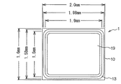
図1、図2において、圧電デバイス1は、絶縁基板としてのセラミック基板10と、セラミック基板10の一方の主面上(上面)に接合された電子部品としての圧電振動片20と、圧電振動片20を覆うようにセラミック基板10上に接合された凹状の金属蓋体19と、を有し、セラミック基板10と金属蓋体19とにより形成されるキャビティーT内に圧電振動片20が気密封止されている。
セラミック基板10と金属蓋体19は、パッケージを構成している。
セラミック基板10は、アルミナから成る平板状のセラミック基材(絶縁基材)11の一方の主面(上面)に圧電振動片20が接合される振動片接合端子18を有し、他方の主面(下面)に複数の外部実装端子16を有している。振動片接合端子18、および、図示しないその他の端子は、セラミック基材11に設けた貫通孔(ビアホール)に高融点金属を含む導体ペーストを埋設することにより形成された層内配線(ビア)17により対応する外部実装端子16に接続されている。
1 and 2, a
The
The
外部実装端子16が設けられたセラミック基板10の一方の主面は圧電デバイス1の外底面となり、その外底面に設けられた外部実装端子16によって、圧電デバイス1を電子機器などの外部実装基板に実装することができる。本実施形態のセラミック基板10を構成するセラミック基材11はグリーンシートを成形・加工してから焼成することにより形成されている。
圧電振動片20は、例えば、水晶などの圧電体材料により形成された平板状の圧電基板の両主面に、対向電極としての励振電極25を設けた構成を有している。また、圧電振動片20の各主面の一端部側には外部接続電極26が設けられ、各々が対応する励振電極25から引き出された電極間配線により電気的に接続されている。なお、圧電振動片20の材質として、水晶以外の圧電体材料では、例えばタンタル酸リチウム、ニオブ酸リチウムなどが挙げられ、また、圧電体材料以外では、シリコンなどを挙げることができる。セラミック基板10上(他方の主面側)において、圧電振動片20は、その一端側に設けられた外部接続電極26をセラミック基板10の対応する振動片接合端子18と位置合わせした状態で、例えば銀ペーストなどの接合部材30により電気的な接続をはかりながら接合され、他端部側を自由端として片持ち支持されている。
金属蓋体19は、その凹部とセラミック基板10の圧電振動片20接合面とで囲まれたキャビティーT内に圧電振動片20を収容させることによって圧電振動片20の搭載領域を気密封止するためのものである。
One main surface of the
The piezoelectric vibrating
The
凹状の金属蓋体19は、例えばコバール、42アロイ、あるいはリン青銅などの金属からなる板材を従来周知の板金加工により成形してなり、中央部下面に凹部(電子部品を収容するための凹部)が形成され、外周部には鍔状の当接脚部19cが環状に形成されている。すなわち、金属蓋体19は、中央部に水平部19aを有し、その水平部19aの外周側から下方へ延びる側壁部19bが形成され、さらに側壁部19bの下縁部を外周側に曲げることにより、金属蓋体19の外周部に水平部19aと略平行な環状の当接脚部19cが形成されている。なお、側壁部19bは図示のように外側へ向かって斜めに傾斜していてもよいし、垂直壁であってもよい。
また、金属蓋体19は、セラミック基板の線膨張係数(7ppm/℃)に近い線膨張係数を有した金属材料であるコバール(線膨張係数:5.5ppm/℃)から成る基材19Aと、基材の下面にクラッド法により積層されたロウ材としての銀ロウ19Bと、基材19Aの上面にクラッド法により積層された酸化防止膜としてのニッケル膜19Cと、から構成されている。なお、基材19Aの材料としては、コバール以外では、42ニッケル、SUSを使用することができる。
The
Further, the
図3に示すように当接脚部19cの下面が接合されるセラミック基板10の外周上面12には、振動片接合端子18と同一材料から成るメタライズ層13が環状に形成されている。メタライズ層13は、セラミック基板を構成するセラミック材料上に振動片接合端子18を形成する際に同時に形成されるため、振動片接合端子18と同一材料から成る。本例では、メタライズ層13は、セラミック基材11上に成膜された銅等の導体から成る配線材料13aと、配線材料上にニッケル膜13bを介して成膜された金膜13cと、から構成されている。
金属蓋体19は、水平部19aと側壁部19bとにより形成される凹部の開口部側をセラミック基板10側に向けた状態で、当接脚部19cをセラミック基板10のメタライズ層13に対向させて接合されている。そして、図3に示すように、セラミック基板10の外周上面の環状のメタライズ層13と、金属蓋体19の環状の当接脚部19cの下面とが、例えば、比較的低融点の合金からなる接合部材としてのロウ材層19Bを溶融、固化させることにより接合されている。
As shown in FIG. 3, a
The
また、金属蓋体19は、メタライズ層13を介してセラミック基板10の図示しないグランド端子に電気的に接続されることが好ましい。このようにすれば、圧電デバイス1の使用時に、金属からなる金属蓋体19がグランド電位に保持されることにより、圧電振動片20を金属蓋体19のシールド効果によって外部からの不要な電気的作用、例えばノイズなどから保護することができる。
かくして上述した圧電デバイス1は、セラミック基板10の底面に設けられた外部実装端子16を介して圧電振動片20の両主面に設けられた励振電極25間に外部からの変動電圧を印加し、圧電振動片20の特性に応じた所定の周波数で振動を起こさせることによって圧電デバイス1として機能し、かかる圧電デバイス1の共振周波数に基づいて外部の発振回路で所定周波数の基準信号を発振・出力することができる。そして、このような基準信号は、例えば携帯用通信機器などの電子機器におけるクロック信号として利用することができる。
The
Thus, the
本発明の圧電デバイス1の特徴的な構成は、セラミック基材(絶縁基材)11、及びセラミック基材上に形成されたメタライズ層13を備えたセラミック基板(絶縁基板)10と、絶縁基板の一面上に接合された電子部品20と、メタライズ層13上にロウ材19Bを介して周縁(当接脚部19c)を接合されることにより電子部品を封止する金属蓋体19と、を備え、メタライズ層13は、当接脚部19c(金属蓋体周縁部)下面と接合する接合領域13Aと、当接脚部19cよりも外側に位置する外周上面12上に張り出し形成した張出し領域(当接脚部により覆われていない領域、或いは金属蓋体周縁部より外側に見えているメタライズ層)13Bと、を備えている点にある。張出し領域13Bがセラミック基材11上に張出す位置は、図示のようにセラミック基材の端縁の手前であってもよいし、セラミック基材の端縁まで延在していてもよい。
なお、メタライズ層13を予め接合領域13Aと張出し領域13Bに厳密に分けて設計する訳ではなく、メタライズ層上に金属蓋体の当接脚部16cを位置決め載置した結果として、当接脚部下面と対向する(接する)メタライズ層の部分が接合領域13Aとなり、当接脚部の外側端縁よりも外側に位置するメタライズ層部分が張出し領域13Bとなる。
A characteristic configuration of the
It should be noted that the metallized
また、メタライズ層13の接合領域13A上にロウ材19Bを介して当接脚部19c(基材19A下面)を配置してからレーザー光、ハロゲンランプの光(加熱用の光)、又は電子ビームを照射してロウ材を溶融させることにより両部材13、19cを接合する際に、接合領域13A、及び張出し領域13Bにレーザー光を同時に照射することによって張出し領域13Bに対する加熱を同時に行って、ロウ材の濡れ性を高めて(溶融の確実化と、展開する範囲の拡大)接合不良箇所の発生を防止する点が特徴的である。
レーザー光を接合領域13Aに相当する当接脚部19cの上面のみに照射する場合にはメタライズ層13の昇温が不十分となるためにロウ材19Bが十分に溶融しない状態で冷却固化することがあり、その部分は接合不良箇所となって気密性が低下する。これに対して本発明では、当接脚部19cよりも外側へ張り出した張出し領域(当接脚部により覆われていない領域)13Bをレーザー光により照射して加熱するため、メタライズ層の昇温が不十分となることがなくなる。
Further, after the
When only the upper surface of the
また、セラミック基材のレーザー光吸収率は30%と高いために、波長が1070〜1090nm程度のレーザー光を当接脚部19cに照射する際に外周上面12に直接照射すると発熱によってセラミック基材がダメージを受けて劣化して不良品となる虞が高まるが、本発明のように当接脚部10cよりも外側の外周上面12上をメタライズ層の張出し領域13Bによってカバーした構成とすることによって、レーザー光がセラミック基材上に照射される虞を無くすることができる。
なお、レーザー光のスポット径を小さく絞ったり、照射位置精度を高めることによって、セラミック基材へ照射されることを防止することは可能であるが、生産性の低下をもたらす虞がある。
本発明ではメタライズ層13の表層にレーザー光の吸収率が5%程度である金膜13cが形成されていることにより、レーザー光の大半は反射され、金膜に吸収されるのは5%程度である。このため、メタライズ層の直下に位置するセラミック基材が熱によって劣化することが防止される一方で、メタライズ層13はレーザー光によって十分に加熱されるので、メタライズ層の全部、又は一部の昇温不足を原因としてロウ材19Bの溶融不良が発生することも防止できる。
Further, since the laser light absorption rate of the ceramic base material is as high as 30%, when the laser beam having a wavelength of about 1070 to 1090 nm is irradiated to the
Although it is possible to prevent the ceramic base material from being irradiated by reducing the spot diameter of the laser beam or by increasing the irradiation position accuracy, there is a risk that productivity will be reduced.
In the present invention, since the
また、個々のセラミック基材上のメタライズ層上に対する金属蓋体の当接脚部19cの位置決めに多少のずれ、バラツキが生じたとしても、メタライズ層の面積をセラミック基材の端縁に向けて十分に拡張しているので、位置ずれを吸収して十分な強度で接合することができる。
更に、張出し領域13Bを設けることにより、ロウ材の溶融状態が十分な場合には当接脚部19cの裏面に積層されているロウ材が張出し領域13B上に染み出して展開してくるので、当接脚部の外周縁からはみ出したロウ材の量を確認することにより、接合状態の良否を外観により判断することが可能となり、検査し易くなる。
In addition, even if there is a slight shift or variation in the positioning of the
Furthermore, by providing the
なお、メタライズ層13と振動片接合端子18の構成材料が同一となる理由は、セラミック基板の製造工程にある。即ち、配線パターンを有したセラミック基材11は、焼成前のグリーンシート上に配線材料(導体ペースト)を印刷したものを焼成することによって形成されており、グリーンシートの同一面上に形成される振動片接合端子18とメタライズ層13は、前記配線材料の印刷工程において同時に塗布され、焼成されることによりセラミック基材11と一体化する。
しかし、このようにグリーンシートを高温により焼成することによりセラミック基材11面に配線材料を一体化する製造方法では、銅を配線材料として使用することが難しかった。
The reason why the constituent materials of the metallized
However, in the manufacturing method in which the wiring material is integrated with the surface of the
そこで、近年セラミック基板面に、高温加熱を伴わないセミアディティブ法を用いて銅配線を形成する方法が開発されている。この方法は、グリーンシートに配線材料のペーストを印刷してから焼成するのではなく、焼成済みのグリーンシートにフォトリソグラフィ技術を用いてメッキ、スパッタ、エッチングを順次行うことにより、任意の銅配線を酸化させずに形成するものである。
本発明では、このセミアディティブ法を用いることによって、焼成済みのグリーンシートに対して後から、メタライズ層13と振動片接合端子18を含む銅配線を形成する場合を含むものである。
Therefore, in recent years, a method of forming a copper wiring on a ceramic substrate surface by using a semi-additive method without high temperature heating has been developed. This method does not print the wiring material paste on the green sheet and then fires it, but performs plating, sputtering, and etching on the fired green sheet in order using photolithography technology, thereby forming an arbitrary copper wiring. It is formed without being oxidized.
In the present invention, by using this semi-additive method, a case where a copper wiring including the metallized
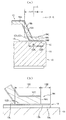
次に、図3に基づいてメタライズ層13と金属蓋体19との接合部の構造について詳細に説明する。
レーザー光によりメタライズ層と金属蓋体の当接脚部19cを溶接する場合のレーザー光の照射位置は、図3(a)に示すようにレーザー光のスポット径の中心部Cが当接脚部19cの幅寸法W1(接合部13Aの幅寸法)の中心部とほぼ合致するように設定する。この際、メタライズ層の張出し領域13Bの少なくとも一部がレーザー光のスポット径内に含まれるようにレーザー光のスポット径を大きく設定することにより、張出し領域13Bを同時に加熱することができ、当接脚部裏面のロウ材19Bを確実に溶融させることにより、当接脚部を越えて張出し領域13B上に展開させることが可能となる。
Next, the structure of the joint between the metallized
As shown in FIG. 3 (a), the laser beam irradiation position when the metallized layer and the metal
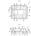
次に、図4(a)及び(b)は本発明の他の実施形態に係る電子デバイスの一例としての圧電デバイスの縦断面図、及び要部拡大図である。
この圧電デバイス40が前記実施形態に係る圧電デバイスと異なる点は、セラミック基板10が平板状ではなく、上面中央部に凹陥部41を有し、凹陥部41を包囲するように環状外枠42が形成されている構成にある。なお、図1の圧電デバイスと同一部材には同一符号を付して説明する。
セラミック基板10は、セラミック基材11の下面に複数の外部実装端子16を有し、他方の主面に設けた凹陥部41の内底面に圧電振動片20が接合される振動片接合端子18を有している。振動片接合端子18、および、図示しないその他の端子は、層内配線(ビア)17により対応する外部実装端子16に接続されている。
Next, FIGS. 4A and 4B are a longitudinal sectional view and a main part enlarged view of a piezoelectric device as an example of an electronic device according to another embodiment of the present invention.
The piezoelectric device 40 is different from the piezoelectric device according to the above embodiment in that the
The
圧電振動片20は、その一端側に設けられた外部接続電極を対応する振動片接合端子18と位置合わせした状態で、例えば銀ペーストなどの接合部材30により電気的な接続をはかりながら接合され、他端部側を自由端として片持ち支持されている。
平板状の金属蓋体19は、例えばコバール、42アロイ、あるいはリン青銅などの金属から構成する。
金属蓋体19は、セラミック基板の線膨張係数(7ppm/℃)に近い線膨張係数を有した金属材料であるコバール(線膨張係数:5.5ppm/℃)から成る基材19Aと、基材の下面にクラッド法により積層されたロウ材としての銀ロウ19Bと、基材19Aの上面にクラッド法により積層された酸化防止膜としてのニッケル膜19Cと、から構成されている。なお、基材19Aの材料としては、コバール以外では、42ニッケル、SUSを使用することができる。
The piezoelectric vibrating
The
The
セラミック基板の環状外枠42の上面には、メタライズ層13が形成されている。メタライズ層13は、当接脚部19c(金属蓋体周縁部)下面と接合する接合領域13Aと、当接脚部19cよりも外側に位置する外周上面12上に張り出し形成した張出し領域(当接脚部により覆われていない領域)13Bと、を備えている。張出し領域13Bがセラミック基材11上に張出す位置は、図示のようにセラミック基材の端縁の手前であってもよいし、セラミック基材の端縁まで延在していてもよい。
本例では、メタライズ層13は、セラミック基材11上に成膜された銅等の導体から成る配線材料13aと、配線材料上にニッケル膜13bを介して成膜された金膜13cと、から構成されている。
金属蓋体19は、外周下面をメタライズ層13と当接させた状態で、レーザー光、或いは電子ビームを図4(b)に示したように照射して銀ロウ19Bを溶融、固化させることによって、環状外枠42の上面に接合一体化される。金属枠体の下面のうちでメタライズ層13と当接して接合される領域は接合領域13Aであり、接合領域よりも外側に位置するメタライズ部分は張出し領域13Bを構成している。
A metallized
In this example, the metallized
The
本実施形態では、図4(b)に示すように、セラミック基板10の環状外枠42上面全体に形成されたメタライズ層13と、金属蓋体19の下面とが、例えば、比較的低融点の合金からなる接合部材としての銀ロウ19Bを介して接合されている。
本実施形態の圧電デバイス40においても、金属蓋体とセラミック基材とを接合するために金属蓋体の外周部上面にレーザー光を照射する際に、レーザー光の一部をメタライズ層13の張出し部13Bの少なくとも一部にも照射することにより、張出し部13Bを適度な温度まで昇温させることができる。このため、接合領域13Aと接する銀ロウ19Bをばらつきなく溶融温度まで昇温させることができ、接合不良による気密性の低下を防止することができる。また、溶融した銀ロウの一部は昇温した状態にある張出し領域13Bまで展開することができるため、外観観察によって接合状態の良否を判定することができる。
特に、メタライズ層13の表層にレーザー光の反射率が高い金膜13cを設けたため、メタライズ層への蓄熱によって直下のセラミック部分が過剰に加熱されることによる劣化を防止することができる。
In this embodiment, as shown in FIG. 4B, the metallized
Also in the piezoelectric device 40 of the present embodiment, when laser light is irradiated on the upper surface of the outer peripheral portion of the metal lid in order to join the metal lid and the ceramic substrate, a part of the laser light is projected from the metallized
In particular, since the
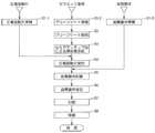
次に、図5は本発明に係る圧電デバイスの製造方法の一例を示すフローチャートである。また、図6はグリーンシートによりセラミック基板を製造する過程を示す平面図である。
なお、本例では図1、図2に示した電子デバイスの製造方法を説明するが、図4に係る電子デバイスについても同等の手順による製造が可能である。
本発明に係る電子デバイスの製造方法の概略は次の通りである。
即ち、電子部品20と、環状のメタライズ層13を備えている絶縁基板10と、及び金属蓋体19を夫々準備する工程と、前記絶縁基板上に前記電子部品を接合する工程と、前記絶縁基板上に前記金属蓋体の周縁部を前記環状のメタライズ層が見えるように配置して前記電子部品を収容する工程と、前記金属蓋体側から前記周縁部、及び前記周縁部より外側に見えている前記メタライズ層(張出し領域13B)に加熱用の光、又は電子ビームを照射して接合する工程と、を有している。
Next, FIG. 5 is a flowchart showing an example of a method for manufacturing a piezoelectric device according to the present invention. FIG. 6 is a plan view showing a process of manufacturing a ceramic substrate using a green sheet.
In this example, the manufacturing method of the electronic device shown in FIGS. 1 and 2 will be described. However, the electronic device according to FIG. 4 can be manufactured by the same procedure.
The outline of the manufacturing method of the electronic device according to the present invention is as follows.
That is, a step of preparing an
圧電デバイス1の製造工程は、圧電振動片20、セラミック基板10、および金属蓋体19をそれぞれ準備する前工程と、セラミック基板10上に圧電振動片20を接合してから金属蓋体19を接合して圧電振動片20を気密封止する後工程(組立工程)とに大別することができる。まず、前工程のうち、圧電振動片20、および金属蓋体19の準備について概略を説明する。
ステップS1−1に示す圧電振動片20準備では、圧電振動片20を製造して圧電デバイス1組立ができる形態にする。圧電振動片20は、例えば水晶などの圧電体材料を所定のサイズに切り出して研磨した大判のウェハーに複数並べて一括形成することができる。
The manufacturing process of the
In the preparation of the piezoelectric vibrating
概要を説明すると、まず、結晶軸に対して所定のカット角で切り出してから所望の厚さおよび表面状態となるように研磨加工した大判の水晶基板(水晶ウェハー)を準備する。そして、フォトリソグラフィを用いたウェットエッチングにより、水晶基板に複数の圧電振動片20の外形を形成する。
なお、圧電振動片20の外形は、水晶基板から完全に切り離されないようにミシン目状の折り取り部などにより水晶ウェハーにつなげたまま、以降の工程を水晶基板(ウェハー)状態にて効率的に流動することが好ましい。そして、スパッタリングや蒸着などによって、励振電極25や外部接続電極26などの電極形成を行うことにより、水晶ウェハーに複数の圧電振動片20がマトリクス状に形成される。
ステップS1−3に示す金属蓋体19準備では、金属蓋体19を製造して圧電デバイス1組立ができる形態にする。金属蓋体19は、例えば、42アロイやコバール、あるいはリン青銅などの金属からなる板状の基材19Aの表面にニッケル膜19Cを、裏面に銀ロウ19Bを夫々クラッド法により積層一体化した構成を有し、従来周知の板金加工により成形することによって、中央部に凹部が形成され、外周部に当接脚部19cが環状に設けられた金属蓋体19を形成する。
The outline will be described. First, a large crystal substrate (crystal wafer) which is cut out at a predetermined cut angle with respect to the crystal axis and then polished to have a desired thickness and surface state is prepared. Then, the outer shape of the plurality of piezoelectric vibrating
In addition, the outer shape of the piezoelectric vibrating
In the preparation of the
次に、セラミック基板10の製造から圧電デバイス1組立までの製造工程を続けて説明する。
本実施形態では、セラミック基板10の基材としてセラミックのグリーンシート51が用いられており、セラミック基板10の製造では、ステップS1−2において準備したグリーンシートをステップS2において焼成する。次いで、ステップS3において焼成済みのグリーンシートに対してセミアディティブ法を用いてメタライズ層13、振動片接合端子18、外部実装端子19を夫々銅を用いて形成する。なお、メタライズ層13を構成する銅13aの表面には酸化防止のためにニッケル薄膜13b、金薄膜13cを順次積層形成する。
以上、ステップS1−2のグリーンシート51準備からステップS2、S3までのステップにより、セラミック基板10がマトリクス状に複数形成されたグリーンシートが完成する(図6を参照)。
なお、この段階で、グリーンシート51から個片のセラミック基板10に分割することもできる。例えば、複数の圧電デバイス形成領域1Aがマトリクス状に形成されたグリーンシート51を、圧電デバイス形成領域1A間に形成される縦横のダイシングラインに沿ってダイシングすることなどにより、個片のセラミック基板10を得ることができる。
Next, the manufacturing process from manufacturing the
In the present embodiment, a ceramic green sheet 51 is used as a base material of the
As described above, a green sheet in which a plurality of
At this stage, the green sheet 51 can be divided into individual
本実施形態では、複数のセラミック基板10が形成されたグリーンシート51の状態のままで、圧電デバイス1の組立を効率的に行う方法について、以下、説明する。
圧電デバイス組立工程では、まず、ステップS4に示すように、グリーンシート51の各圧電デバイス形成領域1Aに、上記ステップS1−1で準備した圧電振動片20を接合する。具体的には、まず、各圧電デバイス形成領域1Aの振動片接合端子18上に、ディスペンサーやスクリーン印刷などにより銀ペーストなどの接合部材39を塗布してから、圧電振動片20の一端側に設けられた外部接続電極26を、対応する振動片接合端子18に位置合わせして仮止めする。そして、接合部材39の硬化方法に応じた処理、例えば、熱硬化型の接合部材39であれば所定の温度で加熱し、また、紫外線硬化型の接合部材であれば紫外線を照射することにより接合部材39を固化させて、圧電振動片20を片持ち支持された態様に接合する。
In the present embodiment, a method for efficiently assembling the
In the piezoelectric device assembly process, first, as shown in step S4, the piezoelectric vibrating
次に、ステップS5において、圧電振動片20が接合された大面積のグリーンシート51の各圧電デバイス形成領域1Aに夫々個片としての金属蓋体19を配置する。金属蓋体19の当接脚部19cの下面の銀ロウ19Bは、セラミック基板上のメタライズ層13と互いに整合する位置関係で位置決めされている。
次に、ステップS6の金属蓋体接合工程においては、図3に示したように当接脚部19cの上面に向けて所要スポット径を有したレーザー光を照射して銀ロウ19Bを加熱溶融させることにより、金属蓋体19による圧電振動片20の気密封止をより強固で確実なものとすることができる。この際に、レーザー光の一部をメタライズ層の張出し領域13Bにも照射して十分に昇温させることにより、銀ロウ19Bの昇温バラツキにより接合不良を解消する。
Next, in step S5, the
Next, in the metal lid joining process of step S6, as shown in FIG. 3, the laser beam having a required spot diameter is irradiated toward the upper surface of the
なお、上述した一連のセラミック基板10への金属蓋体接合ステップ(ステップS5の金属蓋体配置、および、ステップS6の金属蓋体接合)は、例えば、窒素ガスやアルゴンガスなどの不活性ガス雰囲気、あるいは減圧空間内で行うことが好ましい。これによって、圧電振動片20が収納されるセラミック基板10と金属蓋体19とにより形成されるキャビティーTの内部が不活性ガスが充満され、あるいは減圧空間に密閉・封止されるので、圧電振動片20が酸素や大気中の水分などによって腐食・劣化するのを有効に防止することができる。
以上、説明した一連のステップを経て、グリーンシート51に、複数の圧電デバイス1がマトリクス状に形成される。
Note that the above-described series of metal lid joining steps to the ceramic substrate 10 (metal lid arrangement in step S5 and metal lid joining in step S6) are performed in an inert gas atmosphere such as nitrogen gas or argon gas, for example. Or it is preferable to carry out in a decompression space. As a result, the inside of the cavity T formed by the
As described above, the plurality of
次に、ステップS7の分割工程において、上述したステップS6までのステップを経たグリーンシート51を分割して複数の個片の圧電デバイス1を同時に得る。
分割ステップにより得られた圧電デバイス1は、ステップS8において、電気的特性や外観品質の検査を行なうことにより完成され、一連の圧電デバイス1の製造工程を終了する。
上記実施形態の圧電デバイスの製造方法によれば、絶縁基板上に金属蓋体を接合する工程において、メタライズ層の接合領域上にロウ材を介して金属蓋体周縁部を配置してから、金属蓋体側から接合領域、及び張出し領域にレーザー光を照射するようにしたので、金属蓋体19による圧電振動片20の気密封止をより強固で確実なものとすることができる。この際に、レーザー光の一部をメタライズ層の張出し領域13Bにも照射して十分に昇温させることにより、銀ロウ19Bの昇温バラツキにより接合不良を解消することができる。
Next, in the dividing step of step S7, the green sheet 51 that has undergone the steps up to step S6 described above is divided to obtain a plurality of pieces of
The
According to the piezoelectric device manufacturing method of the above embodiment, in the step of joining the metal lid on the insulating substrate, the metal lid peripheral portion is disposed on the joining region of the metallized layer via the brazing material, and then the metal Since the laser beam is irradiated from the lid side to the joining region and the overhanging region, the hermetic sealing of the piezoelectric vibrating
特に、金属蓋体の外周縁全周に渡って溶接を行うレーザー照射において、セラミック基板面の非平坦性がメタライズ層にも反映されているため、レーザー照射した場合にはロウ材の溶融の良否にバラツキが出る。このバラツキを解消するために、本発明ではメタライズ層の張出し領域までをも加熱してその温度を高めて、ロウ材を全周方向に渡って確実に溶かして濡れ性を高め、密着性を高めることができる。
特に、メタライズ層表面に金膜を設けることにより、その直下のセラミックが過熱されることがなくなり、ダメージをなくすることができる。
上記実施形態および変形例で説明した特定の形態、例えば、セラミック基板10、あるいは電子部品としての圧電振動片20などの形状は限定されるものではない。
同様に、各電極、配線、端子などの位置や形状についても上記実施形態およびに限定されない。
また、上記実施形態および変形例では、電子デバイスの一例として、電子部品としての圧電振動片20を搭載した圧電デバイス1、40について説明した。しかし、これに限らず、上記実施形態および変形例に示す構成は、電子部品として半導体回路素子など種々の電子部品を基板に接合し、その電子部品を金属蓋体により気密封止する構造の様々な電子デバイスのパッケージ構造に適用することができる。
In particular, in laser irradiation where welding is performed over the entire outer periphery of the metal lid, the non-flatness of the ceramic substrate surface is also reflected in the metallized layer. The variation comes out. In order to eliminate this variation, in the present invention, even the overhanging region of the metallized layer is heated to increase its temperature, and the brazing material is surely melted in the entire circumferential direction to improve wettability and improve adhesion. be able to.
In particular, by providing a gold film on the surface of the metallized layer, the ceramic immediately below it is not overheated, and damage can be eliminated.
The specific forms described in the above embodiments and modifications, for example, the shape of the
Similarly, the position and shape of each electrode, wiring, terminal, etc. are not limited to the above embodiment.
In the embodiment and the modification, the
具体的には例えば、水晶振動子等の圧電振動子のパッケージのキャビティーT内部、或いはパッケージ外部に発振回路を構成する半導体回路素子を組み込んだ圧電発振器のパッケージ構造に対しても本発明を適用することができる。
即ち、図7は本発明の電子デバイスの他の構成例としての圧電発振器を示す断面図である。なお、図1、図2と同一部分には同一符号を付して説明する。
図7に示すように、水晶振動子等の圧電振動子のパッケージのキャビティーT内部、或いはパッケージ外部に発振回路を構成する半導体回路素子61を組み込んだ圧電発振器60のパッケージ構造に対しても本発明を適用することができる。
この圧電発振器においても、絶縁基板上に金属蓋体を接合する工程において、メタライズ層の接合領域上に、ロウ材を介して金属蓋体周縁部を配置してから、金属蓋体側から接合領域、及び張出し領域にレーザー光を照射するようにしたので、金属蓋体19による圧電振動片20の気密封止をより強固で確実なものとすることができる。この際に、レーザー光の一部をメタライズ層の張出し領域13Bにも照射して十分に昇温させることにより、銀ロウ19Bの昇温バラツキにより接合不良を解消することができる。
Specifically, for example, the present invention is applied to a package structure of a piezoelectric oscillator in which a semiconductor circuit element constituting an oscillation circuit is incorporated inside a cavity T of a package of a piezoelectric vibrator such as a crystal vibrator or outside the package. can do.
That is, FIG. 7 is a sectional view showing a piezoelectric oscillator as another configuration example of the electronic device of the present invention. In addition, the same code | symbol is attached | subjected and demonstrated to the same part as FIG. 1, FIG.
As shown in FIG. 7, the present invention is also applied to a package structure of a
Also in this piezoelectric oscillator, in the step of joining the metal lid on the insulating substrate, the metal lid peripheral edge is disposed on the metallized layer joining region via the brazing material, and then the joining region from the metal lid side, Since the overhanging region is irradiated with laser light, the hermetic sealing of the piezoelectric vibrating
次に、図8は本発明に係る電子機器の構成を示す概略構成図である。電子機器70は上記の圧電デバイス1、40を備えている。圧電デバイス1,40を用いた電子機器70としては、伝送機器等を挙げることができる。これらの電子機器70において圧電デバイスは、基準信号源、或いは電圧可変型圧電発振器(VCXO)等として用いられ、小型で、良好な電子機器を提供できる。
Next, FIG. 8 is a schematic configuration diagram showing the configuration of the electronic apparatus according to the present invention. The
1…圧電デバイス、10…セラミック基板、11…セラミック基材、12…外周上面、13…メタライズ層、13A…接合領域、13B…張出し領域、13a…配線材料(銅膜)、13b…ニッケル膜、13c…金膜、16…外部実装端子、18…振動片接合端子、19…金属蓋体、19A…基材、19B…ロウ材(銀ロウ)、19C…ニッケル膜、19a…水平部、19b…側壁部、19c…当接脚部、20…圧電振動片、25…励振電極、26…外部接続電極、30…接合部材、40…圧電デバイス、41…凹陥部、42…環状外枠、51…グリーンシート、60…圧電発振器、61…半導体回路素子、70電子機器
DESCRIPTION OF
Claims (6)
電子部品と、環状のメタライズ層を備えている絶縁基板と、及び金属蓋体を夫々準備する工程と、
前記絶縁基板上に前記電子部品を接合する工程と、
前記絶縁基板上に前記金属蓋体の周縁部を前記環状のメタライズ層が見えるように配置して前記電子部品を収容する工程と、
前記金属蓋体側から前記周縁部、及び前記周縁部より外側に見えている前記メタライズ層に加熱用の光、又は電子ビームを照射して接合する工程と、
を有していることを特徴とする電子デバイスの製造方法。 An electronic device manufacturing method comprising:
A step of preparing an electronic component, an insulating substrate having an annular metallization layer, and a metal lid, respectively;
Bonding the electronic component on the insulating substrate;
A step of accommodating the electronic component by arranging a peripheral portion of the metal lid on the insulating substrate so that the annular metallized layer can be seen; and
A step of irradiating the metallized layer, which is visible from the metal lid side to the outer peripheral part and the outer peripheral part, by irradiating heating light or an electron beam; and
The manufacturing method of the electronic device characterized by having.
前記金属蓋体は、前記電子部品を収容するための凹部を有していることを特徴とする電子デバイス。 It is an electronic device manufactured by the manufacturing method of the electronic device of Claim 1, Comprising: The one surface which joined the said electronic component is a flat surface, as for the said insulation base material,
The electronic device is characterized in that the metal lid has a recess for accommodating the electronic component.
半導体素子を備えていることを特徴とする圧電発振器。 The electronic device according to any one of claims 2, 3, and 4 is a piezoelectric vibrator,
A piezoelectric oscillator comprising a semiconductor element.
Priority Applications (1)
| Application Number | Priority Date | Filing Date | Title |
|---|---|---|---|
| JP2012000502A JP2013140876A (en) | 2012-01-05 | 2012-01-05 | Manufacturing method of electronic device, electronic device, piezoelectric oscillator, and electronic apparatus |
Applications Claiming Priority (1)
| Application Number | Priority Date | Filing Date | Title |
|---|---|---|---|
| JP2012000502A JP2013140876A (en) | 2012-01-05 | 2012-01-05 | Manufacturing method of electronic device, electronic device, piezoelectric oscillator, and electronic apparatus |
Publications (2)
| Publication Number | Publication Date |
|---|---|
| JP2013140876A true JP2013140876A (en) | 2013-07-18 |
| JP2013140876A5 JP2013140876A5 (en) | 2015-01-29 |
Family
ID=49038081
Family Applications (1)
| Application Number | Title | Priority Date | Filing Date |
|---|---|---|---|
| JP2012000502A Withdrawn JP2013140876A (en) | 2012-01-05 | 2012-01-05 | Manufacturing method of electronic device, electronic device, piezoelectric oscillator, and electronic apparatus |
Country Status (1)
| Country | Link |
|---|---|
| JP (1) | JP2013140876A (en) |
Cited By (2)
| Publication number | Priority date | Publication date | Assignee | Title |
|---|---|---|---|---|
| JP2018113716A (en) * | 2018-03-12 | 2018-07-19 | セイコーエプソン株式会社 | Electronic device, circuit board for electronic device, electronic apparatus, and movable body |
| JP2020036179A (en) * | 2018-08-30 | 2020-03-05 | 日本電波工業株式会社 | Piezoelectric device |
Citations (2)
| Publication number | Priority date | Publication date | Assignee | Title |
|---|---|---|---|---|
| JP2004179373A (en) * | 2002-11-27 | 2004-06-24 | Kinseki Ltd | Electronic parts package and its sealing method |
| JP2011066651A (en) * | 2009-09-17 | 2011-03-31 | Kyocera Kinseki Corp | Piezoelectric device |
-
2012
- 2012-01-05 JP JP2012000502A patent/JP2013140876A/en not_active Withdrawn
Patent Citations (2)
| Publication number | Priority date | Publication date | Assignee | Title |
|---|---|---|---|---|
| JP2004179373A (en) * | 2002-11-27 | 2004-06-24 | Kinseki Ltd | Electronic parts package and its sealing method |
| JP2011066651A (en) * | 2009-09-17 | 2011-03-31 | Kyocera Kinseki Corp | Piezoelectric device |
Cited By (2)
| Publication number | Priority date | Publication date | Assignee | Title |
|---|---|---|---|---|
| JP2018113716A (en) * | 2018-03-12 | 2018-07-19 | セイコーエプソン株式会社 | Electronic device, circuit board for electronic device, electronic apparatus, and movable body |
| JP2020036179A (en) * | 2018-08-30 | 2020-03-05 | 日本電波工業株式会社 | Piezoelectric device |
Similar Documents
| Publication | Publication Date | Title |
|---|---|---|
| US20070008051A1 (en) | Electronic component and manufacturing method thereof | |
| TW201521359A (en) | Surface mounting quartz crystal unit | |
| JP2014067849A (en) | Method for manufacturing electronic device container, method for manufacturing electronic device, electronic equipment, and mobile equipment | |
| KR20090048539A (en) | Piezoelectric vibration device | |
| JP2011147054A (en) | Electronic apparatus, and method of manufacturing the same | |
| JP5251224B2 (en) | Method for manufacturing piezoelectric vibration device and piezoelectric vibration device | |
| JP2013140876A (en) | Manufacturing method of electronic device, electronic device, piezoelectric oscillator, and electronic apparatus | |
| JP2009033613A (en) | Lid body aggregate, piezoelectric vibration device using the lid body aggregate concerned, and manufacturing method of the piezoelectric vibration device | |
| JP4893578B2 (en) | Electronic component sealing method | |
| JP5171228B2 (en) | Crystal device for surface mounting | |
| JP2006332599A (en) | Electronic device | |
| JP5915179B2 (en) | Electronic device, oscillator, method for manufacturing electronic device, and method for manufacturing oscillator | |
| JP2013140874A (en) | Electronic device, ceramic substrate, manufacturing method, and piezoelectric oscillator | |
| JP2007318209A (en) | Surface mounted piezoelectric vibrating device, and manufacturing method thereof | |
| JP2002084159A (en) | Surface-mounted piezoelectric vibrator | |
| JP2008186917A (en) | Electronic component housing package, electronic device, and manufacturing method thereof | |
| JP2012015779A (en) | Method for manufacturing piezoelectric vibrator, and piezoelectric vibrator | |
| JP4380419B2 (en) | Manufacturing method of electronic device | |
| JP4992686B2 (en) | Piezoelectric vibration device and method for manufacturing piezoelectric vibration device | |
| JP2009239475A (en) | Surface mounting piezoelectric oscillator | |
| JP5432533B2 (en) | Manufacturing method of electronic device | |
| JP2001144201A (en) | Electronic part | |
| JP5407903B2 (en) | Electronic device and method of manufacturing electronic device | |
| JP4893602B2 (en) | Piezoelectric vibration device and hermetic sealing method of piezoelectric vibration device | |
| JP2004088036A (en) | Electronic device and its manufacturing method |
Legal Events
| Date | Code | Title | Description |
|---|---|---|---|
| A521 | Written amendment |
Free format text: JAPANESE INTERMEDIATE CODE: A523 Effective date: 20141204 |
|
| A621 | Written request for application examination |
Free format text: JAPANESE INTERMEDIATE CODE: A621 Effective date: 20141204 |
|
| RD04 | Notification of resignation of power of attorney |
Free format text: JAPANESE INTERMEDIATE CODE: A7424 Effective date: 20150107 |
|
| A977 | Report on retrieval |
Free format text: JAPANESE INTERMEDIATE CODE: A971007 Effective date: 20150813 |
|
| A131 | Notification of reasons for refusal |
Free format text: JAPANESE INTERMEDIATE CODE: A131 Effective date: 20150818 |
|
| A761 | Written withdrawal of application |
Free format text: JAPANESE INTERMEDIATE CODE: A761 Effective date: 20151005 |