JP5381821B2 - Protective tape peeling method and protective tape peeling apparatus - Google Patents
Protective tape peeling method and protective tape peeling apparatus Download PDFInfo
- Publication number
- JP5381821B2 JP5381821B2 JP2010053447A JP2010053447A JP5381821B2 JP 5381821 B2 JP5381821 B2 JP 5381821B2 JP 2010053447 A JP2010053447 A JP 2010053447A JP 2010053447 A JP2010053447 A JP 2010053447A JP 5381821 B2 JP5381821 B2 JP 5381821B2
- Authority
- JP
- Japan
- Prior art keywords
- protective tape
- wafer
- peeling
- tape
- lift pin
- Prior art date
- Legal status (The legal status is an assumption and is not a legal conclusion. Google has not performed a legal analysis and makes no representation as to the accuracy of the status listed.)
- Expired - Fee Related
Links
Images


Classifications
-
- B—PERFORMING OPERATIONS; TRANSPORTING
- B65—CONVEYING; PACKING; STORING; HANDLING THIN OR FILAMENTARY MATERIAL
- B65H—HANDLING THIN OR FILAMENTARY MATERIAL, e.g. SHEETS, WEBS, CABLES
- B65H3/00—Separating articles from piles
- B65H3/32—Separating articles from piles by elements, e.g. fingers, plates, rollers, inserted or traversed between articles to be separated and remainder of the pile
-
- B—PERFORMING OPERATIONS; TRANSPORTING
- B32—LAYERED PRODUCTS
- B32B—LAYERED PRODUCTS, i.e. PRODUCTS BUILT-UP OF STRATA OF FLAT OR NON-FLAT, e.g. CELLULAR OR HONEYCOMB, FORM
- B32B43/00—Operations specially adapted for layered products and not otherwise provided for, e.g. repairing; Apparatus therefor
- B32B43/006—Delaminating
-
- B—PERFORMING OPERATIONS; TRANSPORTING
- B32—LAYERED PRODUCTS
- B32B—LAYERED PRODUCTS, i.e. PRODUCTS BUILT-UP OF STRATA OF FLAT OR NON-FLAT, e.g. CELLULAR OR HONEYCOMB, FORM
- B32B38/00—Ancillary operations in connection with laminating processes
- B32B38/10—Removing layers, or parts of layers, mechanically or chemically
-
- H—ELECTRICITY
- H01—ELECTRIC ELEMENTS
- H01L—SEMICONDUCTOR DEVICES NOT COVERED BY CLASS H10
- H01L21/00—Processes or apparatus adapted for the manufacture or treatment of semiconductor or solid state devices or of parts thereof
- H01L21/67—Apparatus specially adapted for handling semiconductor or electric solid state devices during manufacture or treatment thereof; Apparatus specially adapted for handling wafers during manufacture or treatment of semiconductor or electric solid state devices or components ; Apparatus not specifically provided for elsewhere
- H01L21/67005—Apparatus not specifically provided for elsewhere
- H01L21/67011—Apparatus for manufacture or treatment
- H01L21/67132—Apparatus for placing on an insulating substrate, e.g. tape
-
- B—PERFORMING OPERATIONS; TRANSPORTING
- B32—LAYERED PRODUCTS
- B32B—LAYERED PRODUCTS, i.e. PRODUCTS BUILT-UP OF STRATA OF FLAT OR NON-FLAT, e.g. CELLULAR OR HONEYCOMB, FORM
- B32B2457/00—Electrical equipment
- B32B2457/14—Semiconductor wafers
-
- H—ELECTRICITY
- H01—ELECTRIC ELEMENTS
- H01L—SEMICONDUCTOR DEVICES NOT COVERED BY CLASS H10
- H01L21/00—Processes or apparatus adapted for the manufacture or treatment of semiconductor or solid state devices or of parts thereof
- H01L21/67—Apparatus specially adapted for handling semiconductor or electric solid state devices during manufacture or treatment thereof; Apparatus specially adapted for handling wafers during manufacture or treatment of semiconductor or electric solid state devices or components ; Apparatus not specifically provided for elsewhere
- H01L21/683—Apparatus specially adapted for handling semiconductor or electric solid state devices during manufacture or treatment thereof; Apparatus specially adapted for handling wafers during manufacture or treatment of semiconductor or electric solid state devices or components ; Apparatus not specifically provided for elsewhere for supporting or gripping
- H01L21/6835—Apparatus specially adapted for handling semiconductor or electric solid state devices during manufacture or treatment thereof; Apparatus specially adapted for handling wafers during manufacture or treatment of semiconductor or electric solid state devices or components ; Apparatus not specifically provided for elsewhere for supporting or gripping using temporarily an auxiliary support
- H01L21/6836—Wafer tapes, e.g. grinding or dicing support tapes
-
- H—ELECTRICITY
- H01—ELECTRIC ELEMENTS
- H01L—SEMICONDUCTOR DEVICES NOT COVERED BY CLASS H10
- H01L2221/00—Processes or apparatus adapted for the manufacture or treatment of semiconductor or solid state devices or of parts thereof covered by H01L21/00
- H01L2221/67—Apparatus for handling semiconductor or electric solid state devices during manufacture or treatment thereof; Apparatus for handling wafers during manufacture or treatment of semiconductor or electric solid state devices or components; Apparatus not specifically provided for elsewhere
- H01L2221/683—Apparatus for handling semiconductor or electric solid state devices during manufacture or treatment thereof; Apparatus for handling wafers during manufacture or treatment of semiconductor or electric solid state devices or components; Apparatus not specifically provided for elsewhere for supporting or gripping
- H01L2221/68304—Apparatus for handling semiconductor or electric solid state devices during manufacture or treatment thereof; Apparatus for handling wafers during manufacture or treatment of semiconductor or electric solid state devices or components; Apparatus not specifically provided for elsewhere for supporting or gripping using temporarily an auxiliary support
- H01L2221/68327—Apparatus for handling semiconductor or electric solid state devices during manufacture or treatment thereof; Apparatus for handling wafers during manufacture or treatment of semiconductor or electric solid state devices or components; Apparatus not specifically provided for elsewhere for supporting or gripping using temporarily an auxiliary support used during dicing or grinding
-
- H—ELECTRICITY
- H01—ELECTRIC ELEMENTS
- H01L—SEMICONDUCTOR DEVICES NOT COVERED BY CLASS H10
- H01L2221/00—Processes or apparatus adapted for the manufacture or treatment of semiconductor or solid state devices or of parts thereof covered by H01L21/00
- H01L2221/67—Apparatus for handling semiconductor or electric solid state devices during manufacture or treatment thereof; Apparatus for handling wafers during manufacture or treatment of semiconductor or electric solid state devices or components; Apparatus not specifically provided for elsewhere
- H01L2221/683—Apparatus for handling semiconductor or electric solid state devices during manufacture or treatment thereof; Apparatus for handling wafers during manufacture or treatment of semiconductor or electric solid state devices or components; Apparatus not specifically provided for elsewhere for supporting or gripping
- H01L2221/68304—Apparatus for handling semiconductor or electric solid state devices during manufacture or treatment thereof; Apparatus for handling wafers during manufacture or treatment of semiconductor or electric solid state devices or components; Apparatus not specifically provided for elsewhere for supporting or gripping using temporarily an auxiliary support
- H01L2221/68381—Details of chemical or physical process used for separating the auxiliary support from a device or wafer
- H01L2221/68386—Separation by peeling
-
- Y—GENERAL TAGGING OF NEW TECHNOLOGICAL DEVELOPMENTS; GENERAL TAGGING OF CROSS-SECTIONAL TECHNOLOGIES SPANNING OVER SEVERAL SECTIONS OF THE IPC; TECHNICAL SUBJECTS COVERED BY FORMER USPC CROSS-REFERENCE ART COLLECTIONS [XRACs] AND DIGESTS
- Y10—TECHNICAL SUBJECTS COVERED BY FORMER USPC
- Y10S—TECHNICAL SUBJECTS COVERED BY FORMER USPC CROSS-REFERENCE ART COLLECTIONS [XRACs] AND DIGESTS
- Y10S156/00—Adhesive bonding and miscellaneous chemical manufacture
- Y10S156/918—Delaminating processes adapted for specified product, e.g. delaminating medical specimen slide
- Y10S156/93—Semiconductive product delaminating, e.g. delaminating emiconductive wafer from underlayer
- Y10S156/931—Peeling away backing
- Y10S156/932—Peeling away backing with poking during delaminating, e.g. jabbing release sheet backing to remove wafer
-
- Y—GENERAL TAGGING OF NEW TECHNOLOGICAL DEVELOPMENTS; GENERAL TAGGING OF CROSS-SECTIONAL TECHNOLOGIES SPANNING OVER SEVERAL SECTIONS OF THE IPC; TECHNICAL SUBJECTS COVERED BY FORMER USPC CROSS-REFERENCE ART COLLECTIONS [XRACs] AND DIGESTS
- Y10—TECHNICAL SUBJECTS COVERED BY FORMER USPC
- Y10S—TECHNICAL SUBJECTS COVERED BY FORMER USPC CROSS-REFERENCE ART COLLECTIONS [XRACs] AND DIGESTS
- Y10S156/00—Adhesive bonding and miscellaneous chemical manufacture
- Y10S156/934—Apparatus having delaminating means adapted for delaminating a specified article
- Y10S156/941—Means for delaminating semiconductive product
- Y10S156/943—Means for delaminating semiconductive product with poking delaminating means, e.g. jabbing means
-
- Y—GENERAL TAGGING OF NEW TECHNOLOGICAL DEVELOPMENTS; GENERAL TAGGING OF CROSS-SECTIONAL TECHNOLOGIES SPANNING OVER SEVERAL SECTIONS OF THE IPC; TECHNICAL SUBJECTS COVERED BY FORMER USPC CROSS-REFERENCE ART COLLECTIONS [XRACs] AND DIGESTS
- Y10—TECHNICAL SUBJECTS COVERED BY FORMER USPC
- Y10T—TECHNICAL SUBJECTS COVERED BY FORMER US CLASSIFICATION
- Y10T156/00—Adhesive bonding and miscellaneous chemical manufacture
- Y10T156/11—Methods of delaminating, per se; i.e., separating at bonding face
- Y10T156/1168—Gripping and pulling work apart during delaminating
- Y10T156/1179—Gripping and pulling work apart during delaminating with poking during delaminating [e.g., jabbing, etc.]
-
- Y—GENERAL TAGGING OF NEW TECHNOLOGICAL DEVELOPMENTS; GENERAL TAGGING OF CROSS-SECTIONAL TECHNOLOGIES SPANNING OVER SEVERAL SECTIONS OF THE IPC; TECHNICAL SUBJECTS COVERED BY FORMER USPC CROSS-REFERENCE ART COLLECTIONS [XRACs] AND DIGESTS
- Y10—TECHNICAL SUBJECTS COVERED BY FORMER USPC
- Y10T—TECHNICAL SUBJECTS COVERED BY FORMER US CLASSIFICATION
- Y10T156/00—Adhesive bonding and miscellaneous chemical manufacture
- Y10T156/19—Delaminating means
- Y10T156/1978—Delaminating bending means
- Y10T156/1983—Poking delaminating means
Landscapes
- Engineering & Computer Science (AREA)
- Mechanical Engineering (AREA)
- Physics & Mathematics (AREA)
- Condensed Matter Physics & Semiconductors (AREA)
- General Physics & Mathematics (AREA)
- Manufacturing & Machinery (AREA)
- Computer Hardware Design (AREA)
- Microelectronics & Electronic Packaging (AREA)
- Power Engineering (AREA)
- Container, Conveyance, Adherence, Positioning, Of Wafer (AREA)
Description
本発明は、ウエハに貼り付けられた保護テープを剥離する保護テープ剥離方法および保護テープ剥離装置に関する。 The present invention relates to a protective tape peeling method and a protective tape peeling device for peeling a protective tape attached to a wafer.
半導体電子デバイスには高機能化および省エネルギー化とともに小型化が要求される。半導体電子デバイスの小型化のために、ウエハを薄く研削することがある。ウエハを薄く研削する際には、ウエハ表面を保護するためにウエハ表面に保護テープが貼り付けられる。ウエハを研削した後も、ウエハの強度を高く維持するために、ウエハに保護テープが貼り付けられたまま処理が進められる。つまり、保護テープによりウエハ強度が高められ、ウエハハンドリングを安全に行うことができる。この保護テープは最終的には保護テープ剥離装置を使って剥離する。具体的には、保護テープに剥離用粘着テープが貼り付けられる。そして、剥離用粘着テープをウエハ外部方向へ引っ張る。これにより剥離用粘着テープとそれに貼り付けられた保護テープをウエハから剥がす。 Semiconductor electronic devices are required to be miniaturized with high functionality and energy saving. In order to reduce the size of semiconductor electronic devices, the wafer may be ground thinly. When grinding a wafer thinly, a protective tape is attached to the wafer surface in order to protect the wafer surface. Even after the wafer is ground, in order to keep the strength of the wafer high, the process proceeds while the protective tape is stuck on the wafer. That is, the wafer strength is increased by the protective tape, and the wafer handling can be performed safely. This protective tape is finally peeled off using a protective tape peeling device. Specifically, an adhesive tape for peeling is attached to the protective tape. Then, the peeling adhesive tape is pulled toward the outside of the wafer. Thus, the peeling adhesive tape and the protective tape attached thereto are peeled off from the wafer.
ウエハ表面にパターンの段差が少ない場合やパターンの段差が無い場合には、ウエハ表面と保護テープとの密着性が高い。そのため、剥離用粘着テープと保護テープとの間の接着力が、ウエハ表面と保護テープとの間の接着力より低くなり、剥離用粘着テープが保護テープから剥がれることがあった。その結果、保護テープをウエハ表面から剥離できないことがあった。この問題を解消するために、ウエハのノッチにおいて、応力付加手段により保護テープをウエハ表面から離れるように持ち上げた状態で、保護テープを剥離する技術が提案されている(例えば、特許文献1参照)。 When there are few pattern steps on the wafer surface or when there are no pattern steps, the adhesion between the wafer surface and the protective tape is high. Therefore, the adhesive force between the peeling adhesive tape and the protective tape is lower than the adhesive force between the wafer surface and the protective tape, and the peeling adhesive tape may be peeled off from the protective tape. As a result, the protective tape may not be peeled from the wafer surface. In order to solve this problem, a technique has been proposed in which the protective tape is peeled off at the notch of the wafer while the protective tape is lifted away from the wafer surface by stress applying means (see, for example, Patent Document 1). .
保護テープは必ずしもウエハの外縁に沿って貼り付けられるとは限らない。保護テープがウエハの外縁の内側に貼り付けられる場合もある。その場合、保護テープのノッチと重なる部分の面積が非常に小さいため、応力付加手段を用いても当該部分をウエハ表面から持ち上げることができない。 The protective tape is not necessarily applied along the outer edge of the wafer. In some cases, a protective tape is attached to the inside of the outer edge of the wafer. In that case, since the area of the portion overlapping the notch of the protective tape is very small, the portion cannot be lifted from the wafer surface even if stress applying means is used.
また、保護テープがウエハの外縁よりも外側にはみ出すように貼り付けられる場合もある。その場合、保護テープのノッチと重なる部分を応力付加手段により押すだけでは、保護テープを十分に持ち上げることができない。このように保護テープがウエハの外縁に沿って貼り付けられていない場合に、保護テープをウエハから剥離できないという問題があった。 In some cases, the protective tape is attached so as to protrude outside the outer edge of the wafer. In that case, the protective tape cannot be sufficiently lifted by simply pressing the portion overlapping the notch of the protective tape with the stress applying means. As described above, there is a problem that the protective tape cannot be peeled off from the wafer when the protective tape is not attached along the outer edge of the wafer.
本発明は、上述のような課題を解決するためになされたもので、保護テープがウエハの外縁に沿って貼り付けられていない場合でも保護テープをウエハから容易に剥離できる保護テープ剥離方法および保護テープ剥離装置を提供することを目的とする。 The present invention has been made in order to solve the above-described problems, and a protective tape peeling method and protection capable of easily peeling a protective tape from a wafer even when the protective tape is not attached along the outer edge of the wafer. It aims at providing a tape peeling apparatus.
本発明にかかる保護テープ剥離方法は、ウエハのノッチを覆う第1の部分と該ウエハの外縁より外側へはみ出す第2の部分とを有する保護テープが貼り付けられた該ウエハを、ステージに載せる工程と、剥離用粘着テープを該保護テープに貼り付ける工程と、該ステージからリフトピンを突出させて、該リフトピンの上面により該第1の部分および該第2の部分を持ち上げる工程と、該リフトピンにより該保護テープを持ち上げた状態で該剥離用粘着テープを引っ張り、該保護テープを該ウエハから剥離する工程とを備え、該リフトピンの上面形状は、幅狭部と幅広部を有し、該幅狭部が該第1の部分を持ち上げ、該幅広部が該第2の部分を持ち上げることを特徴とする。 The method for peeling off the protective tape according to the present invention includes a step of placing the wafer, to which a protective tape having a first part covering the notch of the wafer and a second part protruding outside the outer edge of the wafer, is attached, on a stage A step of attaching a peeling adhesive tape to the protective tape, a step of projecting a lift pin from the stage and lifting the first part and the second part by the upper surface of the lift pin, and the lift pin A step of pulling the peeling adhesive tape in a state where the protective tape is lifted to peel the protective tape from the wafer, and the top surface of the lift pin has a narrow portion and a wide portion, and the narrow portion Lifts the first part, and the wide part lifts the second part.
本発明にかかる保護テープ剥離装置は、ウエハのノッチを覆う第1の部分と該ウエハの外縁より外側へはみ出す第2の部分とを有する保護テープが貼り付けられた該ウエハを載せるステージと、該保護テープに剥離用粘着テープを貼り付ける手段と、該剥離用粘着テープを剥離する手段と、該ステージから突出することが可能なように該ステージに取り付けられたリフトピンとを備え、該リフトピンの上面形状は、幅狭部と幅広部を有し、該幅狭部が該第1の部分を持ち上げ、該幅広部が該第2の部分を持ち上げることができる形状であることを特徴とする。 The protective tape peeling apparatus according to the present invention includes a stage on which the wafer to which a protective tape having a first portion covering the notch of the wafer and a second portion protruding outward from the outer edge of the wafer is attached, A means for attaching a peeling adhesive tape to the protective tape; a means for peeling the peeling adhesive tape; and a lift pin attached to the stage so as to be able to protrude from the stage. The shape has a narrow portion and a wide portion, and the narrow portion can lift the first portion, and the wide portion can lift the second portion.
本発明によれば、保護テープがウエハの外縁に沿って貼り付けられていない場合でも保護テープをウエハから容易に剥離できる。 According to the present invention, the protective tape can be easily peeled from the wafer even when the protective tape is not attached along the outer edge of the wafer.
実施の形態1.
本発明の実施の形態1にかかる保護テープ剥離方法および保護テープ剥離装置について図1ないし図13を参照して説明する。なお、同一又は対応する構成要素には同一の符号を付して説明の繰り返しを省略する場合がある。他の実施の形態でも同様である。
Embodiment 1 FIG.
A protective tape peeling method and a protective tape peeling device according to Embodiment 1 of the present invention will be described with reference to FIGS. In addition, the same code | symbol may be attached | subjected to the same or corresponding component, and description of description may be abbreviate | omitted. The same applies to other embodiments.
図1は実施の形態1にかかるウエハ10を示す平面図である。ウエハ10の外縁部にはノッチ12が形成されている。ノッチ12は、ウエハ10の結晶方向の判別をしたり、位置決めをしたりするための切り欠きである。
FIG. 1 is a plan view showing a
図2は実施の形態1にかかる保護テープ14とウエハ10の位置関係を示す平面図である。ウエハ10の端面はグラインダーなどにより面取り加工される。これによりウエハ10の強度が上がり、ウエハ10の端面への物理的な衝撃による割れや欠けを抑制できる。この面取り加工をするために、保護テープ14はウエハ10の外縁よりも例えば0.5mmから1.0mm程度、内側の位置に貼り付けられる(以下、この保護テープ貼り付け方法を「内張り」と呼ぶ)。保護テープ14はノッチ12の一部のみと重なるようにウエハ10に貼り付けられるがノッチ12の全部とは重ならない。
FIG. 2 is a plan view showing the positional relationship between the
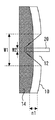
図3は実施の形態1にかかる保護テープ剥離装置16を示す断面図である。保護テープ剥離装置16は、ウエハ10を搭載するステージ18と、ステージ18から突出することが可能なようにステージ18に取り付けられたリフトピン20とを備える。リフトピン20は保護テープ14を持ち上げるものである。また、リフトピン20は図3に示されるようにステージ18内に収納されることができる。図4は実施の形態1にかかるリフトピン20を示す斜視図である。リフトピン20の上面は長方形である。
FIG. 3 is a cross-sectional view illustrating the protective
保護テープ剥離装置16は、さらに剥離用粘着テープ22を貼り付ける手段を備える。この手段は剥離用粘着テープ22を支持するローラ24とスキージ26を備える。なお、この剥離用粘着テープ22を貼り付ける手段は、剥離用粘着テープ22を剥離する手段でもある。
The protective
図5は、実施の形態1にかかる保護テープ剥離方法を説明するフローチャートである。以後、このフローチャートに沿って実施の形態1の保護テープ剥離方法について説明する。 FIG. 5 is a flowchart for explaining the protective tape peeling method according to the first embodiment. Hereinafter, the protective tape peeling method according to the first embodiment will be described with reference to this flowchart.
まず、図6に示すように、保護テープ14が貼り付けられたウエハ10をステージ18上に載せる(ステップ50)。ウエハ10は保護テープ14が貼り付けられた面と反対の面でステージ18と接する。また、ウエハ10はステージ18上に真空吸着によって固定される。
First, as shown in FIG. 6, the
図7は、実施の形態1にかかるリフトピン20、ウエハ10および保護テープ14との位置関係を示す平面図である。リフトピン20の上面は長方形である。この、リフトピン20の上面の一部がノッチ12と重なるように、ウエハ10をステージ18上に配置する。ここでリフトピン20の上面の幅はノッチ12の開口幅W1未満であり、ノッチ12の最小幅W2以下であることが好ましい。このようにリフトピン20の上面の幅を狭くするとリフトピン20をノッチ12の奥まで届くように配置できる。なお、図7におけるn1は保護テープ14の外縁とウエハ10の外縁の差を表わす。n1はたとえば0.5mmから1.0mm程度である。ステップ50ではこのように、ノッチ12の一部のみと重なるように保護テープ14が貼り付けられたウエハ10をステージ18上に載せる。具体的には、ノッチ12における保護テープ14の直下にリフトピン20が位置するようにウエハ10をステージ18上へ載せる。
FIG. 7 is a plan view showing the positional relationship between the lift pins 20, the
ステップ50を終えるとステップ51へと処理が進められる。ステップ51では、剥離用粘着テープ22を保護テープ14に貼り付ける。図8に示すように、保護テープ14の高さに合わせてスキージ26を移動させて、剥離用粘着テープ22を保護テープ14に貼り付ける。この動作は、図9に示すように剥離用粘着テープ22が保護テープ14を横断するように貼り付けられるまで継続する。剥離用粘着テープ22の貼り付けが完了すると、いったんローラ24およびスキージ26の動作を停止させる。
When
ステップ51を終えるとステップ52へと処理が進められる。ステップ52では図10に示すように、ステージ18からリフトピン20を突出させて、リフトピン20の上面によりノッチ12における保護テープ14を持ち上げる。このとき、長方形に形成されたリフトピン20の上面が保護テープ14と接する。図11は実施の形態1にかかるリフトピン20の突出する前の状態を示す断面図である。図12は実施の形態1にかかるリフトピン20の突出した後の状態を示す断面図である。
When
ステップ52を終えるとステップ53へと処理が進められる。ステップ53ではリフトピン20により保護テープ14を持ち上げた状態で剥離用粘着テープ22を引っ張り、保護テープ14をウエハ10から剥離する。具体的には、剥離用粘着テープ22を剥離用粘着テープ22が貼り付けられた方向と反対の方向へ引っ張る。つまり、剥離用粘着テープ22を図10における左側方向へ引っ張る。剥離用粘着テープ22を引っ張ると剥離用粘着テープ22に密着した保護テープ14も引っ張られる。よって、剥離用粘着テープ22と保護テープ14をまとめてウエハ10から剥離できる。
When step 52 is completed, the process proceeds to step 53. In
ステップ53では、リフトピン20により持ち上げられた部分を基点として保護テープ14の剥離が進められる。最終的に、図13に示すようにすべての保護テープ14をウエハ10から剥離してステップ53を終了する。実施の形態1の保護テープ剥離方法および保護テープ剥離装置は上述のとおりである。
In
実施の形態1のように保護テープ14が「内張り」されている場合は、ノッチ12の一部にのみ保護テープ14が配置される。そのような場合であっても、リフトピン20がノッチ12の奥まで届くように配置されるため、保護テープ14とリフトピン20の接触面積を大きくすることができる。よってノッチ12部分における保護テープ14を確実にリフトピン20で持ち上げることができる。ゆえに、ウエハ10の表面と保護テープ14との密着性が高い場合においても保護テープ14を確実に剥離することができる。
When the
なお、ノッチ12はSEMIスタンダード(SEMI規格)で定められた形状である場合が多い。この場合は、リフトピン20の上面の形状を3mm×1.2cmとする。つまり、リフトピン20の幅が図7におけるノッチの最小幅W2以下となるように、その幅として3mmを選択する。当然、リフトピン20の幅は3mm以下でもよい。一方、リフトピン20の長さは1.2cmに限らず適宜定めればよい。
In many cases, the
実施の形態1ではリフトピン20をステージ18から突出させた後に剥離用粘着テープ22の引っ張りを開始したが、本発明はこれに限定されない。リフトピン20の突出と同時に剥離用粘着テープ22の引っ張りを開始してもよい。また、剥離用粘着テープ22の引っ張りを開始した後にリフトピン20を上昇させてもよい。
In Embodiment 1, the lift-off
実施の形態1ではリフトピン20の上面形状が長方形であることとしたが、本発明はこれに限定されない。リフトピン20の上面形状は、リフトピン20の上面がノッチ12における保護テープ14を持ち上げることができる形状であればよい。よってリフトピン20の上面形状はたとえば三角形や円形でもよい。
In the first embodiment, the top surface of the
実施の形態2.
本発明の実施の形態2にかかる保護テープ剥離方法および保護テープ剥離装置について図14ないし図16を参照して説明する。実施の形態1と同様の構成要素には同じ符号を用いる。以後、実施の形態1との相違点を中心に説明する。
Embodiment 2. FIG.
A protective tape peeling method and a protective tape peeling device according to a second embodiment of the present invention will be described with reference to FIGS. The same reference numerals are used for the same components as those in the first embodiment. Hereinafter, the description will focus on differences from the first embodiment.
図14は実施の形態2にかかる保護テープ70とウエハ10の位置関係を示す平面図である。ウエハ10は実施の形態1と同様にノッチ12を有する。保護テープ70は、ウエハ10の外縁よりも外側へはみ出すように貼り付けられている。したがって、保護テープ70は、ノッチ12を覆う第1の部分と、ウエハ10の外縁より外側へはみ出す第2の部分とを有する。保護テープ70がウエハ10の外縁よりも外側へはみ出すのは、ウエハ10端面への物理的な衝撃による割れや欠けを防止するためである。このように保護テープ70をウエハ10に貼り付けることを「外張り」という。
FIG. 14 is a plan view showing the positional relationship between the
図15は実施の形態2にかかるリフトピン72を示す斜視図である。リフトピン72の上面形状は幅広部74と幅狭部76と有する。幅狭部76は半円形状であり、その直径Rは3mmより小さい。
FIG. 15 is a perspective view showing a
実施の形態2にかかる保護テープ剥離方法について説明する。まず、保護テープ70が外張りされたウエハ10をステージ18に載せる。図16は、実施の形態2にかかるリフトピン72と、ウエハ10および保護テープ70との位置関係を示す図である。図16に示されるとおり、リフトピン72の幅狭部76は第1の部分と重なる。また、幅広部74は第2の部分と重なる。
The protective tape peeling method concerning Embodiment 2 is demonstrated. First, the
次に、剥離用粘着テープ22を保護テープ70に貼り付ける。その後、ステージ18からリフトピン72を突出させて、リフトピン72の上面により第1の部分および第2の部分を持ち上げる。リフトピン72が突出すると保護テープ70とリフトピン72は広い面積で接触する。つまり、リフトピン72の上面は第1の部分と第2の部分とを持ち上げる。より詳細には、幅狭部76が第1の部分を持ち上げ、幅広部74が第2の部分を持ち上げる。そして、リフトピン72により保護テープ70を持ち上げた状態で剥離用粘着テープ22を引っ張り、保護テープ70をウエハ10から剥離する。
Next, the peeling
なお、リフトピン72の上面形状は、幅広部74と幅狭部76を有していれば特に限定されない。つまり、幅狭部76が保護テープ70のノッチ12を覆う部分(第1の部分)を持ち上げ、幅広部74が保護テープ70のウエハ10の外縁より外側へはみ出す部分(第2の部分)を持ち上げる限り、本発明の効果を得ることができる。よって、たとえば幅狭部76が長方形になるように形成されていても本発明の効果を得ることができる。その他、実施の形態1相当の変形が可能である。
The shape of the upper surface of the
10 ウエハ、 12 ノッチ、 14,70 保護テープ、 18 ステージ、 20,72 リフトピン、 22 剥離用粘着テープ、 24 ローラ、 26 スキージ 10 wafers, 12 notches, 14,70 protective tape, 18 stages, 20,72 lift pins, 22 peeling adhesive tape, 24 rollers, 26 squeegees
Claims (2)
剥離用粘着テープを前記保護テープに貼り付ける工程と、 A step of attaching an adhesive tape for peeling to the protective tape;
前記ステージからリフトピンを突出させて、前記リフトピンの上面により前記第1の部分および前記第2の部分を持ち上げる工程と、 Projecting lift pins from the stage and lifting the first part and the second part by the upper surface of the lift pins;
前記リフトピンにより前記保護テープを持ち上げた状態で前記剥離用粘着テープを引っ張り、前記保護テープを前記ウエハから剥離する工程とを備え、 A step of pulling the peeling adhesive tape in a state where the protective tape is lifted by the lift pins, and peeling the protective tape from the wafer.
前記リフトピンの上面形状は、幅狭部と幅広部を有し、前記幅狭部が前記第1の部分を持ち上げ、前記幅広部が前記第2の部分を持ち上げることを特徴とする保護テープ剥離方法。 The top surface of the lift pin has a narrow part and a wide part, the narrow part lifts the first part, and the wide part lifts the second part. .
前記保護テープに剥離用粘着テープを貼り付ける手段と、 Means for attaching a peeling adhesive tape to the protective tape;
前記剥離用粘着テープを剥離する手段と、 Means for peeling the peeling adhesive tape;
前記ステージから突出することが可能なように前記ステージに取り付けられたリフトピンとを備え、 A lift pin attached to the stage so that it can protrude from the stage;
前記リフトピンの上面形状は、幅狭部と幅広部を有し、前記幅狭部が前記第1の部分を持ち上げ、前記幅広部が前記第2の部分を持ち上げることができる形状であることを特徴とする保護テープ剥離装置。 The upper surface shape of the lift pin has a narrow portion and a wide portion, and the narrow portion can lift the first portion, and the wide portion can lift the second portion. Protective tape peeling device.
Priority Applications (6)
| Application Number | Priority Date | Filing Date | Title |
|---|---|---|---|
| JP2010053447A JP5381821B2 (en) | 2010-03-10 | 2010-03-10 | Protective tape peeling method and protective tape peeling apparatus |
| TW099146152A TWI431680B (en) | 2010-03-10 | 2010-12-27 | Method and apparatus for peeling protective tape |
| US12/979,844 US20110220296A1 (en) | 2010-03-10 | 2010-12-28 | Method and apparatus for peeling protective tape |
| DE102011004155.9A DE102011004155B4 (en) | 2010-03-10 | 2011-02-15 | Method and device for removing a protective tape |
| CN201110059688.7A CN102205687B (en) | 2010-03-10 | 2011-03-09 | Method and apparatus for peeling protective tape |
| US13/715,218 US8778133B2 (en) | 2010-03-10 | 2012-12-14 | Method and apparatus for peeling protective tape |
Applications Claiming Priority (1)
| Application Number | Priority Date | Filing Date | Title |
|---|---|---|---|
| JP2010053447A JP5381821B2 (en) | 2010-03-10 | 2010-03-10 | Protective tape peeling method and protective tape peeling apparatus |
Publications (2)
| Publication Number | Publication Date |
|---|---|
| JP2011187827A JP2011187827A (en) | 2011-09-22 |
| JP5381821B2 true JP5381821B2 (en) | 2014-01-08 |
Family
ID=44508075
Family Applications (1)
| Application Number | Title | Priority Date | Filing Date |
|---|---|---|---|
| JP2010053447A Expired - Fee Related JP5381821B2 (en) | 2010-03-10 | 2010-03-10 | Protective tape peeling method and protective tape peeling apparatus |
Country Status (5)
| Country | Link |
|---|---|
| US (2) | US20110220296A1 (en) |
| JP (1) | JP5381821B2 (en) |
| CN (1) | CN102205687B (en) |
| DE (1) | DE102011004155B4 (en) |
| TW (1) | TWI431680B (en) |
Families Citing this family (6)
| Publication number | Priority date | Publication date | Assignee | Title |
|---|---|---|---|---|
| CN104779192B (en) * | 2014-01-10 | 2017-10-27 | 上海华虹宏力半导体制造有限公司 | Protection glue cutting method at the wafer gap of grinding processing procedure is thinned for chip back surface |
| JP6301685B2 (en) * | 2014-03-04 | 2018-03-28 | 株式会社ディスコ | Protective tape peeling apparatus and protective tape peeling method |
| TWI685905B (en) * | 2017-07-12 | 2020-02-21 | 日商新川股份有限公司 | Joining device and joining method |
| JP7320932B2 (en) * | 2017-11-10 | 2023-08-04 | 芝浦メカトロニクス株式会社 | Deposition equipment and parts peeling equipment |
| KR102640172B1 (en) | 2019-07-03 | 2024-02-23 | 삼성전자주식회사 | Processing apparatus for a substrate and method of driving the same |
| CN113013080A (en) * | 2021-02-24 | 2021-06-22 | 中芯集成电路制造(绍兴)有限公司 | Film uncovering method |
Family Cites Families (17)
| Publication number | Priority date | Publication date | Assignee | Title |
|---|---|---|---|---|
| EP0848415A1 (en) * | 1995-08-31 | 1998-06-17 | Nitto Denko Corporation | Method and apparatus for peeling protective adhesive tape from semiconductor wafer |
| JPH09115863A (en) * | 1995-10-23 | 1997-05-02 | Oki Electric Ind Co Ltd | Method and apparatus for adhering surface protective tape |
| US6202292B1 (en) * | 1998-08-26 | 2001-03-20 | Micron Technology, Inc. | Apparatus for removing carrier film from a semiconductor die |
| CN1260779C (en) * | 2001-06-11 | 2006-06-21 | 日东电工株式会社 | Method and device for removing useless materials from semiconductor wafers |
| JP2003209082A (en) | 2002-01-15 | 2003-07-25 | Nitto Denko Corp | Sticking method for protecting tape, device therefor and releasing method for protecting tape |
| JP4316187B2 (en) * | 2002-05-20 | 2009-08-19 | リンテック株式会社 | Method and apparatus for peeling brittle material |
| JP2004128147A (en) * | 2002-10-01 | 2004-04-22 | Nitto Denko Corp | Method and device for removing protection tape from semiconductor wafer |
| KR100532287B1 (en) * | 2003-09-17 | 2005-11-29 | 삼성전자주식회사 | Partcle removing apparatus for camera module and method thereof |
| JP4538242B2 (en) * | 2004-01-23 | 2010-09-08 | 株式会社東芝 | Peeling apparatus and peeling method |
| JP4297829B2 (en) * | 2004-04-23 | 2009-07-15 | リンテック株式会社 | Adsorption device |
| US7240422B2 (en) * | 2004-05-11 | 2007-07-10 | Asm Assembly Automation Ltd. | Apparatus for semiconductor chip detachment |
| EP1947688A4 (en) | 2005-11-04 | 2010-10-27 | Tokyo Seimitsu Co Ltd | Film peeling method and film peeling apparatus |
| JP4698517B2 (en) * | 2006-04-18 | 2011-06-08 | 日東電工株式会社 | Protective tape peeling method and apparatus using the same |
| JP4353975B2 (en) * | 2006-11-29 | 2009-10-28 | 日東電工株式会社 | Adhesive sheet sticking / peeling method, adhesive sheet sticking device, and adhesive sheet peeling device |
| JP2009099865A (en) * | 2007-10-18 | 2009-05-07 | Toyota Motor Corp | Removing device and method of removing protective tape |
| JP5061324B2 (en) * | 2007-11-13 | 2012-10-31 | 株式会社タカトリ | Wafer protective tape peeling method and apparatus |
| JP5222756B2 (en) * | 2009-02-24 | 2013-06-26 | リンテック株式会社 | Peeling apparatus and peeling method |
-
2010
- 2010-03-10 JP JP2010053447A patent/JP5381821B2/en not_active Expired - Fee Related
- 2010-12-27 TW TW099146152A patent/TWI431680B/en not_active IP Right Cessation
- 2010-12-28 US US12/979,844 patent/US20110220296A1/en not_active Abandoned
-
2011
- 2011-02-15 DE DE102011004155.9A patent/DE102011004155B4/en not_active Expired - Fee Related
- 2011-03-09 CN CN201110059688.7A patent/CN102205687B/en not_active Expired - Fee Related
-
2012
- 2012-12-14 US US13/715,218 patent/US8778133B2/en not_active Expired - Fee Related
Also Published As
| Publication number | Publication date |
|---|---|
| CN102205687A (en) | 2011-10-05 |
| US20110220296A1 (en) | 2011-09-15 |
| TW201135824A (en) | 2011-10-16 |
| JP2011187827A (en) | 2011-09-22 |
| DE102011004155B4 (en) | 2014-02-13 |
| TWI431680B (en) | 2014-03-21 |
| CN102205687B (en) | 2014-08-06 |
| DE102011004155A1 (en) | 2011-09-15 |
| US20130098542A1 (en) | 2013-04-25 |
| US8778133B2 (en) | 2014-07-15 |
Similar Documents
| Publication | Publication Date | Title |
|---|---|---|
| JP5381821B2 (en) | Protective tape peeling method and protective tape peeling apparatus | |
| KR100766512B1 (en) | Method and device of peeling semiconductor device | |
| TWI353009B (en) | Method for holding semiconductor wafer | |
| JP2008042016A (en) | Holding method of semiconductor wafer, and semiconductor wafer holding structure | |
| US20160071808A1 (en) | Integrated semiconductor device and method for fabricating the same | |
| JP2009044008A (en) | Protective tape peeling method and device for wafer | |
| KR20140138898A (en) | Method and apparatus for temporary bonding ultra thin wafers | |
| US20150262854A1 (en) | Wafer etching system and wafer etching process using the same | |
| JP2009246195A (en) | Adhesive sheet and processing method of semiconductor wafer using the same | |
| JP2010283097A (en) | Double sided adhesive sheet | |
| KR20130138256A (en) | Sheet adhesion device and adhesion method | |
| US20130306215A1 (en) | Adhesive tape ataching method | |
| JP5222756B2 (en) | Peeling apparatus and peeling method | |
| JP5203827B2 (en) | Holding device | |
| JP2006005030A (en) | Method and apparatus for picking up semiconductor chip | |
| JP2013168616A (en) | Protection tape peeling method | |
| JP5214421B2 (en) | Peeling apparatus and peeling method | |
| JP4768963B2 (en) | Wafer transfer method | |
| TW201638257A (en) | Workpiece cutting method | |
| JP2006156567A (en) | Surface protection tape and manufacturing process of semiconductor device | |
| US20190295878A1 (en) | Push-up device and push-up method for a semiconductor device | |
| JP2007073778A (en) | Method and device for picking up semiconductor chip | |
| JP2003273200A (en) | Device and method for stripping tape | |
| JP5319310B2 (en) | Processing apparatus and processing method for plate member | |
| JP2004071687A (en) | Peeling method of adhesive tape for surface protection of semiconductor substrate and peeling tape |
Legal Events
| Date | Code | Title | Description |
|---|---|---|---|
| A621 | Written request for application examination |
Free format text: JAPANESE INTERMEDIATE CODE: A621 Effective date: 20120521 |
|
| A977 | Report on retrieval |
Free format text: JAPANESE INTERMEDIATE CODE: A971007 Effective date: 20130619 |
|
| A131 | Notification of reasons for refusal |
Free format text: JAPANESE INTERMEDIATE CODE: A131 Effective date: 20130625 |
|
| A521 | Request for written amendment filed |
Free format text: JAPANESE INTERMEDIATE CODE: A523 Effective date: 20130724 |
|
| TRDD | Decision of grant or rejection written | ||
| A01 | Written decision to grant a patent or to grant a registration (utility model) |
Free format text: JAPANESE INTERMEDIATE CODE: A01 Effective date: 20130903 |
|
| A61 | First payment of annual fees (during grant procedure) |
Free format text: JAPANESE INTERMEDIATE CODE: A61 Effective date: 20130916 |
|
| R150 | Certificate of patent or registration of utility model |
Free format text: JAPANESE INTERMEDIATE CODE: R150 |
|
| R250 | Receipt of annual fees |
Free format text: JAPANESE INTERMEDIATE CODE: R250 |
|
| LAPS | Cancellation because of no payment of annual fees |