JP5311354B2 - 液晶表示装置 - Google Patents
液晶表示装置 Download PDFInfo
- Publication number
- JP5311354B2 JP5311354B2 JP2011197839A JP2011197839A JP5311354B2 JP 5311354 B2 JP5311354 B2 JP 5311354B2 JP 2011197839 A JP2011197839 A JP 2011197839A JP 2011197839 A JP2011197839 A JP 2011197839A JP 5311354 B2 JP5311354 B2 JP 5311354B2
- Authority
- JP
- Japan
- Prior art keywords
- liquid crystal
- retardation
- display device
- crystal display
- alignment
- Prior art date
- Legal status (The legal status is an assumption and is not a legal conclusion. Google has not performed a legal analysis and makes no representation as to the accuracy of the status listed.)
- Active
Links
Images


Classifications
-
- G—PHYSICS
- G02—OPTICS
- G02F—OPTICAL DEVICES OR ARRANGEMENTS FOR THE CONTROL OF LIGHT BY MODIFICATION OF THE OPTICAL PROPERTIES OF THE MEDIA OF THE ELEMENTS INVOLVED THEREIN; NON-LINEAR OPTICS; FREQUENCY-CHANGING OF LIGHT; OPTICAL LOGIC ELEMENTS; OPTICAL ANALOGUE/DIGITAL CONVERTERS
- G02F1/00—Devices or arrangements for the control of the intensity, colour, phase, polarisation or direction of light arriving from an independent light source, e.g. switching, gating or modulating; Non-linear optics
- G02F1/01—Devices or arrangements for the control of the intensity, colour, phase, polarisation or direction of light arriving from an independent light source, e.g. switching, gating or modulating; Non-linear optics for the control of the intensity, phase, polarisation or colour
- G02F1/13—Devices or arrangements for the control of the intensity, colour, phase, polarisation or direction of light arriving from an independent light source, e.g. switching, gating or modulating; Non-linear optics for the control of the intensity, phase, polarisation or colour based on liquid crystals, e.g. single liquid crystal display cells
- G02F1/133—Constructional arrangements; Operation of liquid crystal cells; Circuit arrangements
- G02F1/1333—Constructional arrangements; Manufacturing methods
- G02F1/1337—Surface-induced orientation of the liquid crystal molecules, e.g. by alignment layers
- G02F1/13378—Surface-induced orientation of the liquid crystal molecules, e.g. by alignment layers by treatment of the surface, e.g. embossing, rubbing or light irradiation
- G02F1/133788—Surface-induced orientation of the liquid crystal molecules, e.g. by alignment layers by treatment of the surface, e.g. embossing, rubbing or light irradiation by light irradiation, e.g. linearly polarised light photo-polymerisation
-
- G—PHYSICS
- G02—OPTICS
- G02F—OPTICAL DEVICES OR ARRANGEMENTS FOR THE CONTROL OF LIGHT BY MODIFICATION OF THE OPTICAL PROPERTIES OF THE MEDIA OF THE ELEMENTS INVOLVED THEREIN; NON-LINEAR OPTICS; FREQUENCY-CHANGING OF LIGHT; OPTICAL LOGIC ELEMENTS; OPTICAL ANALOGUE/DIGITAL CONVERTERS
- G02F1/00—Devices or arrangements for the control of the intensity, colour, phase, polarisation or direction of light arriving from an independent light source, e.g. switching, gating or modulating; Non-linear optics
- G02F1/01—Devices or arrangements for the control of the intensity, colour, phase, polarisation or direction of light arriving from an independent light source, e.g. switching, gating or modulating; Non-linear optics for the control of the intensity, phase, polarisation or colour
- G02F1/13—Devices or arrangements for the control of the intensity, colour, phase, polarisation or direction of light arriving from an independent light source, e.g. switching, gating or modulating; Non-linear optics for the control of the intensity, phase, polarisation or colour based on liquid crystals, e.g. single liquid crystal display cells
- G02F1/133—Constructional arrangements; Operation of liquid crystal cells; Circuit arrangements
- G02F1/1333—Constructional arrangements; Manufacturing methods
- G02F1/1337—Surface-induced orientation of the liquid crystal molecules, e.g. by alignment layers
- G02F1/13378—Surface-induced orientation of the liquid crystal molecules, e.g. by alignment layers by treatment of the surface, e.g. embossing, rubbing or light irradiation
- G02F1/133784—Surface-induced orientation of the liquid crystal molecules, e.g. by alignment layers by treatment of the surface, e.g. embossing, rubbing or light irradiation by rubbing
-
- G—PHYSICS
- G02—OPTICS
- G02F—OPTICAL DEVICES OR ARRANGEMENTS FOR THE CONTROL OF LIGHT BY MODIFICATION OF THE OPTICAL PROPERTIES OF THE MEDIA OF THE ELEMENTS INVOLVED THEREIN; NON-LINEAR OPTICS; FREQUENCY-CHANGING OF LIGHT; OPTICAL LOGIC ELEMENTS; OPTICAL ANALOGUE/DIGITAL CONVERTERS
- G02F1/00—Devices or arrangements for the control of the intensity, colour, phase, polarisation or direction of light arriving from an independent light source, e.g. switching, gating or modulating; Non-linear optics
- G02F1/01—Devices or arrangements for the control of the intensity, colour, phase, polarisation or direction of light arriving from an independent light source, e.g. switching, gating or modulating; Non-linear optics for the control of the intensity, phase, polarisation or colour
- G02F1/13—Devices or arrangements for the control of the intensity, colour, phase, polarisation or direction of light arriving from an independent light source, e.g. switching, gating or modulating; Non-linear optics for the control of the intensity, phase, polarisation or colour based on liquid crystals, e.g. single liquid crystal display cells
- G02F1/133—Constructional arrangements; Operation of liquid crystal cells; Circuit arrangements
- G02F1/1333—Constructional arrangements; Manufacturing methods
- G02F1/1343—Electrodes
- G02F1/134309—Electrodes characterised by their geometrical arrangement
- G02F1/134363—Electrodes characterised by their geometrical arrangement for applying an electric field parallel to the substrate, i.e. in-plane switching [IPS]
Description
[先行技術文献]
[特許文献]
但し、I0は入射光強度、δ=2πΔn・d/λである。
透過光強度が極小になるのは(3)式の条件が成立する場合である。
πΔn・d/λ=m (m=0、1,2、・・・)・・・・・(3)
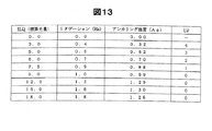
(3)式の関係を用いると、透過率極小波長(λmin)の測定からΔndが求められる。本発明で使用した位相差板は波長550nm近辺において三次の極小(m=3)となるものを使用したので、(3)式は(4)式となる。
二枚の一軸性フィルムを用いた位相差板の合成位相差は、光軸を平行にして積層した場合は両者の和で、また光軸を直交して積層した場合は差で与えられる。ここで、位相差板のΔndをR、測定基板の方位角リタデーションをrとする。測定基板を位相差板の光軸と配向方向を平行にした場合の透過率極小波長をλp、位相差板の光軸と配向方向を直交させた場合の透過率極小波長をλTとすると、上記(4)式から次の(5)式、(6)式が得られる。
R−r=3λT ・・・・・(6)
(5)式から(6)式を引くことにより、(7)式が得られる。
つまり、分光光度計を用いてλpとλTを測定すれば、(7)式から測定基板の方位角リタデーションrが求められる。なおRとrは波長依存性を持つため(7)式は厳密には正しくない。しかし、微小位相差の測定ではλpとλTの値は接近しており(大きくても50nm程度)、位相差板に波長分散の小さいアートンフィルムを使用しているため、50nm程度の波長差での方位角リタデーションの波長依存はほぼ考慮する必要がなく、(7)式は適用可能である。
(3) 遠心分離機の中心軸と直交する方向にセルを固定し遠心分離(500rpm)を3分行い、さらに高圧エアーをセル内に吹き付けることでセル内の液晶を除去した。

Claims (4)
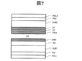
- 一対の基板と、
前記一対の基板のうちの一方の基板上に画素電極と対向電極とが配置され、
前記画素電極と前記対向電極との上方に光照射により配向させた配向膜を有する液晶表示装置であって、
前記配向膜は、光分解型の光配向性ポリイミドからなるものであって、光照射によって1〜80nmの方位角リタデーション値と、光学ツイスト角から得られるアンカリング強度が1.0×10 -3 Jm -2 以上有していることを特徴とした液晶表示装置。 - 請求項1の液晶表示装置において、
白黒チェッカーパターンを2時間表示した後、残像が30分未満で消失することを特徴とした液晶表示装置。 - 請求項1又は2の液晶表示装置において、
前記配向膜は、9.0J/cm 2 以上の光の積算光量を照射して構成されたものである液晶表示装置。 - 請求項1乃至3のいずれかの液晶表示装置において、
前記配向膜は、光分解型の光配向性ポリイミドからなるものであることを特徴とした液晶表示装置。
Priority Applications (1)
| Application Number | Priority Date | Filing Date | Title |
|---|---|---|---|
| JP2011197839A JP5311354B2 (ja) | 2005-11-21 | 2011-09-12 | 液晶表示装置 |
Applications Claiming Priority (3)
| Application Number | Priority Date | Filing Date | Title |
|---|---|---|---|
| JP2005335214 | 2005-11-21 | ||
| JP2005335214 | 2005-11-21 | ||
| JP2011197839A JP5311354B2 (ja) | 2005-11-21 | 2011-09-12 | 液晶表示装置 |
Related Parent Applications (1)
| Application Number | Title | Priority Date | Filing Date |
|---|---|---|---|
| JP2006306765A Division JP5116287B2 (ja) | 2005-11-21 | 2006-11-13 | 液晶表示装置 |
Publications (2)
| Publication Number | Publication Date |
|---|---|
| JP2012027486A JP2012027486A (ja) | 2012-02-09 |
| JP5311354B2 true JP5311354B2 (ja) | 2013-10-09 |
Family
ID=38112272
Family Applications (1)
| Application Number | Title | Priority Date | Filing Date |
|---|---|---|---|
| JP2011197839A Active JP5311354B2 (ja) | 2005-11-21 | 2011-09-12 | 液晶表示装置 |
Country Status (4)
| Country | Link |
|---|---|
| JP (1) | JP5311354B2 (ja) |
| KR (1) | KR100867166B1 (ja) |
| CN (1) | CN1971381B (ja) |
| TW (1) | TW200725124A (ja) |
Families Citing this family (4)
| Publication number | Priority date | Publication date | Assignee | Title |
|---|---|---|---|---|
| RU2011133671A (ru) * | 2009-05-15 | 2013-06-20 | Шарп Кабусики Кайся | Жидкокристаллическое дисплейное устройство |
| WO2016017536A1 (ja) * | 2014-07-31 | 2016-02-04 | シャープ株式会社 | 液晶表示装置 |
| JP6461544B2 (ja) * | 2014-10-08 | 2019-01-30 | 株式会社ジャパンディスプレイ | 液晶表示装置およびその製造方法 |
| WO2017217300A1 (ja) * | 2016-06-14 | 2017-12-21 | シャープ株式会社 | 偏光照射装置及び液晶表示装置の製造方法 |
Family Cites Families (12)
| Publication number | Priority date | Publication date | Assignee | Title |
|---|---|---|---|---|
| JPH04250420A (ja) * | 1991-01-28 | 1992-09-07 | Matsushita Electric Ind Co Ltd | 液晶表示装置およびその製造法 |
| KR0148391B1 (ko) * | 1993-08-31 | 1998-11-16 | 박경팔 | 액정표시소자 |
| JP3075917B2 (ja) * | 1994-05-27 | 2000-08-14 | シャープ株式会社 | 液晶表示装置、その製造方法およびその製造装置 |
| JPH10319409A (ja) * | 1997-05-23 | 1998-12-04 | Hitachi Ltd | アクティブマトリクス型液晶表示装置用の配向膜形成方法 |
| JPH11249142A (ja) * | 1998-03-02 | 1999-09-17 | Hitachi Ltd | 液晶表示装置 |
| JPH11352484A (ja) * | 1998-06-05 | 1999-12-24 | Canon Inc | 液晶素子とその製造方法 |
| JP2000122066A (ja) * | 1998-10-21 | 2000-04-28 | Hitachi Ltd | 液晶表示装置 |
| JP2003255347A (ja) * | 2002-02-27 | 2003-09-10 | Sharp Corp | 液晶表示装置およびその製造方法 |
| JP2004109403A (ja) * | 2002-09-18 | 2004-04-08 | Hitachi Ltd | 液晶表示素子 |
| JP4506333B2 (ja) * | 2003-07-31 | 2010-07-21 | Dic株式会社 | 光学異方体の製造方法 |
| KR100767587B1 (ko) * | 2003-12-30 | 2007-10-17 | 엘지.필립스 엘시디 주식회사 | 코팅형 보상필름을 적용한 액정표시장치 및 그 제조방법 |
| JP4593267B2 (ja) * | 2004-12-28 | 2010-12-08 | 富士通株式会社 | 光ノードおよび光分岐挿入装置 |
-
2006
- 2006-11-20 TW TW095142868A patent/TW200725124A/zh unknown
- 2006-11-20 CN CN2006101495647A patent/CN1971381B/zh active Active
- 2006-11-21 KR KR1020060115262A patent/KR100867166B1/ko active IP Right Grant
-
2011
- 2011-09-12 JP JP2011197839A patent/JP5311354B2/ja active Active
Also Published As
| Publication number | Publication date |
|---|---|
| CN1971381B (zh) | 2012-06-06 |
| KR20070053643A (ko) | 2007-05-25 |
| JP2012027486A (ja) | 2012-02-09 |
| CN1971381A (zh) | 2007-05-30 |
| TW200725124A (en) | 2007-07-01 |
| TWI354842B (ja) | 2011-12-21 |
| KR100867166B1 (ko) | 2008-11-06 |
Similar Documents
| Publication | Publication Date | Title |
|---|---|---|
| JP5116287B2 (ja) | 液晶表示装置 | |
| KR100259111B1 (ko) | 액정표시장치 | |
| WO2015008773A1 (ja) | 位相差フィルム、偏光板および液晶表示装置 | |
| US20070229739A1 (en) | Liquid crystal display device | |
| JP6461544B2 (ja) | 液晶表示装置およびその製造方法 | |
| JP2007183474A (ja) | 液晶表示装置 | |
| JPH10153802A (ja) | 液晶表示装置 | |
| JP2006065285A (ja) | 半透過型表示装置及びその形成方法。 | |
| JP2002040428A (ja) | 液晶表示装置 | |
| JP5311354B2 (ja) | 液晶表示装置 | |
| JP2015018065A (ja) | 液晶表示装置及びその製造方法並びに液晶配向規制力判定方法 | |
| US20040241319A1 (en) | Method of manufacturing phase-difference film using polarized ultraviolet light | |
| US7342628B2 (en) | Liquid crystal display device | |
| JP2006313342A (ja) | Ocbモード液晶表示装置 | |
| JP4610368B2 (ja) | 液晶表示装置用光学素子の製造装置 | |
| JP2010145825A (ja) | 液晶表示装置 | |
| Hong et al. | Novel nematic liquid crystal device associated with hybrid alignment controlled by fringe field | |
| JP2009294320A (ja) | 液晶表示装置 | |
| JP4303075B2 (ja) | 液晶性材料の物性測定方法及び液晶性材料の物性測定装置 | |
| JP2005128359A (ja) | 液晶表示装置 | |
| JP2018036657A (ja) | 位相差フィルム、偏光板および液晶表示装置 | |
| JP2018092046A (ja) | 液晶電気光学素子 | |
| JP2005181826A (ja) | 液晶表示装置および電子機器 | |
| JP2007178496A (ja) | 液晶表示素子 | |
| JP3847772B2 (ja) | 位相差フィルム付偏光板を備える液晶表示パネル |
Legal Events
| Date | Code | Title | Description |
|---|---|---|---|
| A621 | Written request for application examination |
Free format text: JAPANESE INTERMEDIATE CODE: A621 Effective date: 20110912 |
|
| A977 | Report on retrieval |
Free format text: JAPANESE INTERMEDIATE CODE: A971007 Effective date: 20121218 |
|
| A131 | Notification of reasons for refusal |
Free format text: JAPANESE INTERMEDIATE CODE: A131 Effective date: 20130129 |
|
| A521 | Request for written amendment filed |
Free format text: JAPANESE INTERMEDIATE CODE: A523 Effective date: 20130328 |
|
| A521 | Request for written amendment filed |
Free format text: JAPANESE INTERMEDIATE CODE: A523 Effective date: 20130425 |
|
| A521 | Request for written amendment filed |
Free format text: JAPANESE INTERMEDIATE CODE: A523 Effective date: 20130425 |
|
| TRDD | Decision of grant or rejection written | ||
| A01 | Written decision to grant a patent or to grant a registration (utility model) |
Free format text: JAPANESE INTERMEDIATE CODE: A01 Effective date: 20130528 |
|
| A61 | First payment of annual fees (during grant procedure) |
Free format text: JAPANESE INTERMEDIATE CODE: A61 Effective date: 20130625 |
|
| R150 | Certificate of patent or registration of utility model |
Free format text: JAPANESE INTERMEDIATE CODE: R150 Ref document number: 5311354 Country of ref document: JP Free format text: JAPANESE INTERMEDIATE CODE: R150 |
|
| R250 | Receipt of annual fees |
Free format text: JAPANESE INTERMEDIATE CODE: R250 |
|
| R250 | Receipt of annual fees |
Free format text: JAPANESE INTERMEDIATE CODE: R250 |
|
| R250 | Receipt of annual fees |
Free format text: JAPANESE INTERMEDIATE CODE: R250 |
|
| R250 | Receipt of annual fees |
Free format text: JAPANESE INTERMEDIATE CODE: R250 |
|
| R250 | Receipt of annual fees |
Free format text: JAPANESE INTERMEDIATE CODE: R250 |
|
| R250 | Receipt of annual fees |
Free format text: JAPANESE INTERMEDIATE CODE: R250 |
|
| R250 | Receipt of annual fees |
Free format text: JAPANESE INTERMEDIATE CODE: R250 |
|
| R250 | Receipt of annual fees |
Free format text: JAPANESE INTERMEDIATE CODE: R250 |
|
| S111 | Request for change of ownership or part of ownership |
Free format text: JAPANESE INTERMEDIATE CODE: R313117 |
|
| R350 | Written notification of registration of transfer |
Free format text: JAPANESE INTERMEDIATE CODE: R350 |