JP5259807B2 - 半導体装置 - Google Patents
半導体装置 Download PDFInfo
- Publication number
- JP5259807B2 JP5259807B2 JP2011253655A JP2011253655A JP5259807B2 JP 5259807 B2 JP5259807 B2 JP 5259807B2 JP 2011253655 A JP2011253655 A JP 2011253655A JP 2011253655 A JP2011253655 A JP 2011253655A JP 5259807 B2 JP5259807 B2 JP 5259807B2
- Authority
- JP
- Japan
- Prior art keywords
- dielectric substrate
- conductor
- side wall
- base substrate
- circuit pattern
- Prior art date
- Legal status (The legal status is an assumption and is not a legal conclusion. Google has not performed a legal analysis and makes no representation as to the accuracy of the status listed.)
- Expired - Fee Related
Links
Images


Classifications
-
- H—ELECTRICITY
- H03—ELECTRONIC CIRCUITRY
- H03F—AMPLIFIERS
- H03F3/00—Amplifiers with only discharge tubes or only semiconductor devices as amplifying elements
- H03F3/189—High-frequency amplifiers, e.g. radio frequency amplifiers
- H03F3/19—High-frequency amplifiers, e.g. radio frequency amplifiers with semiconductor devices only
- H03F3/195—High-frequency amplifiers, e.g. radio frequency amplifiers with semiconductor devices only in integrated circuits
Landscapes
- Microwave Amplifiers (AREA)
Description
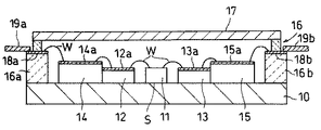
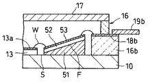
11…半導体素子
12…第1誘電体基板
12a…回路パターン
13…第2誘電体基板
13a…回路パターン
14…第3誘電体基板
14a…線路導体
15…第4誘電体基板
15a…線路導体
16…側壁
17…蓋
18a…入力用帯状導体
18b…出力用帯状導体
19a…入力用リード線
19b…出力用リード線
S…ベース基板の面
Claims (1)
- 金属製ベース基板と、このベース基板上に配置された半導体素子と、前記ベース基板上に配置され、表面に回路パターンを形成した第1誘電体基板と、前記半導体素子および前記第1誘電体基板を囲んで前記ベース基板上に設けた枠状の側壁と、前記側壁の一部に設けられた絶縁物からなる側壁部分と、前記ベース基板の面を基準にして、前記回路パターンよりも高い位置で前記側壁部分を貫通する帯状導体と、前記ベース基板の面を基準にして、前記第1誘電体基板側が低く前記帯状導体側が高くなる傾斜面を有し、前記第1誘電体基板と前記帯状導体との間の前記ベース基板上に設けられた金属ブロックと、この金属ブロック上に設けられ、表面に線路導体パターンが形成された第2誘電体基板と、この第2誘電体基板表面に形成された前記線路導体パターンを介して前記帯状導体と前記回路パターンとの間および前記回路パターンと前記半導体素子との間をそれぞれ接続するワイヤーとを具備したことを特徴とする半導体装置。
Priority Applications (1)
| Application Number | Priority Date | Filing Date | Title |
|---|---|---|---|
| JP2011253655A JP5259807B2 (ja) | 2011-11-21 | 2011-11-21 | 半導体装置 |
Applications Claiming Priority (1)
| Application Number | Priority Date | Filing Date | Title |
|---|---|---|---|
| JP2011253655A JP5259807B2 (ja) | 2011-11-21 | 2011-11-21 | 半導体装置 |
Related Parent Applications (1)
| Application Number | Title | Priority Date | Filing Date |
|---|---|---|---|
| JP2010086000A Division JP5135376B2 (ja) | 2010-04-02 | 2010-04-02 | 半導体装置 |
Publications (2)
| Publication Number | Publication Date |
|---|---|
| JP2012039160A JP2012039160A (ja) | 2012-02-23 |
| JP5259807B2 true JP5259807B2 (ja) | 2013-08-07 |
Family
ID=45850714
Family Applications (1)
| Application Number | Title | Priority Date | Filing Date |
|---|---|---|---|
| JP2011253655A Expired - Fee Related JP5259807B2 (ja) | 2011-11-21 | 2011-11-21 | 半導体装置 |
Country Status (1)
| Country | Link |
|---|---|
| JP (1) | JP5259807B2 (ja) |
Families Citing this family (1)
| Publication number | Priority date | Publication date | Assignee | Title |
|---|---|---|---|---|
| CN114362841B (zh) * | 2021-12-13 | 2023-12-15 | 深圳市卓汉材料技术有限公司 | 一种无源互调测试治具与无源互调测试系统 |
Family Cites Families (4)
| Publication number | Priority date | Publication date | Assignee | Title |
|---|---|---|---|---|
| JPS6114181Y2 (ja) * | 1981-02-25 | 1986-05-02 | ||
| JPS6114183Y2 (ja) * | 1981-02-25 | 1986-05-02 | ||
| JPH0770641B2 (ja) * | 1989-03-17 | 1995-07-31 | 三菱電機株式会社 | 半導体パッケージ |
| JP3735270B2 (ja) * | 2001-05-11 | 2006-01-18 | 松下電器産業株式会社 | 高周波半導体装置 |
-
2011
- 2011-11-21 JP JP2011253655A patent/JP5259807B2/ja not_active Expired - Fee Related
Also Published As
| Publication number | Publication date |
|---|---|
| JP2012039160A (ja) | 2012-02-23 |
Similar Documents
| Publication | Publication Date | Title |
|---|---|---|
| JP4519637B2 (ja) | 半導体装置 | |
| US9978691B2 (en) | Semiconductor packages having wire bond wall to reduce coupling | |
| US9401342B2 (en) | Semiconductor package having wire bond wall to reduce coupling | |
| EP2515435B1 (en) | Power amplifier | |
| JP6273247B2 (ja) | 高周波半導体増幅器 | |
| CN107851635B (zh) | 用于配电的导电密封环 | |
| JP5259807B2 (ja) | 半導体装置 | |
| JP6849060B2 (ja) | 増幅器 | |
| CN104113289B (zh) | 一种微波集成放大器电路及其制作方法 | |
| JP5135376B2 (ja) | 半導体装置 | |
| JP2012039159A (ja) | 半導体装置 | |
| JPWO2007108262A1 (ja) | 送受信装置 | |
| US20140132353A1 (en) | Amplifier circuit | |
| CN114420657B (zh) | 半导体器件和半导体器件的制备方法 | |
| JP2015173234A (ja) | 高周波半導体装置用パッケージおよびその製造方法、並びに高周波半導体装置 | |
| JP5162826B2 (ja) | 半導体装置及びその製造方法 | |
| CN104465616A (zh) | 集成电路的可靠性分析测试结构及其测试方法 | |
| CN106876440A (zh) | 降低soi衬底电容效应的衬底结构及其制备方法 | |
| US11038031B2 (en) | Field-effect transistor | |
| JP5564763B2 (ja) | Mos型半導体装置の製造方法 | |
| CN107039356A (zh) | 微米波段及毫米波段封装体 | |
| CN108109913A (zh) | 双极晶体管的制作方法 | |
| JP2005072954A (ja) | 高周波回路装置 | |
| KR20040081173A (ko) | 회로 칩의 단자를 외부 기준 전위에 도전 접속하는 장치 | |
| CN121772253A (zh) | 一种半导体器件、其制作方法、功率放大器及电子设备 |
Legal Events
| Date | Code | Title | Description |
|---|---|---|---|
| A621 | Written request for application examination |
Free format text: JAPANESE INTERMEDIATE CODE: A621 Effective date: 20111121 |
|
| A977 | Report on retrieval |
Free format text: JAPANESE INTERMEDIATE CODE: A971007 Effective date: 20130118 |
|
| A131 | Notification of reasons for refusal |
Free format text: JAPANESE INTERMEDIATE CODE: A131 Effective date: 20130122 |
|
| A521 | Request for written amendment filed |
Free format text: JAPANESE INTERMEDIATE CODE: A523 Effective date: 20130307 |
|
| TRDD | Decision of grant or rejection written | ||
| A01 | Written decision to grant a patent or to grant a registration (utility model) |
Free format text: JAPANESE INTERMEDIATE CODE: A01 Effective date: 20130402 |
|
| A61 | First payment of annual fees (during grant procedure) |
Free format text: JAPANESE INTERMEDIATE CODE: A61 Effective date: 20130424 |
|
| FPAY | Renewal fee payment (event date is renewal date of database) |
Free format text: PAYMENT UNTIL: 20160502 Year of fee payment: 3 |
|
| LAPS | Cancellation because of no payment of annual fees |