JP5259807B2 - Semiconductor device - Google Patents
Semiconductor device Download PDFInfo
- Publication number
- JP5259807B2 JP5259807B2 JP2011253655A JP2011253655A JP5259807B2 JP 5259807 B2 JP5259807 B2 JP 5259807B2 JP 2011253655 A JP2011253655 A JP 2011253655A JP 2011253655 A JP2011253655 A JP 2011253655A JP 5259807 B2 JP5259807 B2 JP 5259807B2
- Authority
- JP
- Japan
- Prior art keywords
- dielectric substrate
- conductor
- side wall
- base substrate
- circuit pattern
- Prior art date
- Legal status (The legal status is an assumption and is not a legal conclusion. Google has not performed a legal analysis and makes no representation as to the accuracy of the status listed.)
- Expired - Fee Related
Links
Images


Classifications
-
- H—ELECTRICITY
- H03—ELECTRONIC CIRCUITRY
- H03F—AMPLIFIERS
- H03F3/00—Amplifiers with only discharge tubes or only semiconductor devices as amplifying elements
- H03F3/189—High-frequency amplifiers, e.g. radio frequency amplifiers
- H03F3/19—High-frequency amplifiers, e.g. radio frequency amplifiers with semiconductor devices only
- H03F3/195—High-frequency amplifiers, e.g. radio frequency amplifiers with semiconductor devices only in integrated circuits
Landscapes
- Microwave Amplifiers (AREA)
Description
本発明は高周波帯などで使用する半導体装置に関する。 The present invention relates to a semiconductor device used in a high frequency band or the like.
近年、高周波帯などで使用する半導体装置、たとえばガリウム砒素電界効果トランジスタ(以下、GaAsFETという)を用いたマイクロ波電力増幅器などの半導体装置は高出力化が進み、高出力化への対応が求められている。 In recent years, semiconductor devices used in high frequency bands, for example, semiconductor devices such as microwave power amplifiers using gallium arsenide field-effect transistors (hereinafter referred to as GaAsFETs) have been increasing in output and are required to cope with higher output. ing.
ここで、従来の半導体装置について、GaAsFETを用いた半導体装置を例にとり図7を参照して説明する。 Here, a conventional semiconductor device will be described with reference to FIG. 7 taking a semiconductor device using GaAsFET as an example.
金属製ベース基板70上に電力増幅用などの半導体素子71、たとえばGaAsFETが配置されている。半導体素子71のたとえば図示左側に位置する入力側に、第1誘電体基板72が配置されている。第1誘電体基板72上には、たとえば入力側整合回路などを構成する回路パターン72aが形成されている。半導体素子71のたとえば図示右側に位置する出力側に、第2誘電体基板73が配置されている。第2誘電体基板73上には、たとえば出力側整合回路などを構成する回路パターン73aが形成されている。また、半導体素子71および第1誘電体基板72、第2誘電体基板73などを囲んで、ベース基板70上に矩形枠状の側壁74が所定高さに形成されている。側壁74は、たとえば一部を除いて多くの部分が金属で形成され、また上部の矩形状開口はたとえば金属製の蓋75で封止されている。
On a
側壁74の図示左側に位置する入力側側壁部分74aは絶縁物で形成され、その入力側側壁部分74aを入力用帯状導体76aが貫通している。入力用帯状導体76aに入力用リード線77aが接続されている。側壁74の図示右側に位置する出力側側壁部分74bも絶縁物で形成され、その出力側側壁部分74bを出力用帯状導体76bが貫通している。出力用帯状導体76bに出力用リード線77bが接続されている。
The input
また、入力用帯状導体76aと第1誘電体基板72上の回路パターン72aとの間、および、回路パターン72aと半導体素子71との間、半導体素子71と第2誘電体基板73上の回路パターン73aとの間、回路パターン73aと出力用帯状導体76bとの間は、それぞれワイヤーW1〜W4で接続されている。
Further, the circuit pattern on the input strip conductor 76a and the
上記した構成において、入力用帯状導体76aから入力する入力信号は回路パターン72aなどを経て半導体素子71で増幅される。その後、回路パターン73aなどを経て出力用帯状導体76bから出力される。
In the configuration described above, an input signal input from the input strip conductor 76a is amplified by the
上記したような半導体装置、たとえばベース基板上に枠状の側壁を設け、その側壁開口を蓋で覆ったパッケージ内に、半導体素子などを配置する半導体装置は特許文献1などに開示されている。 A semiconductor device as described above, for example, a semiconductor device in which a semiconductor element or the like is arranged in a package in which a frame-like side wall is provided on a base substrate and the side wall opening is covered with a lid is disclosed in Patent Document 1 and the like.
従来の半導体装置は高出力化に伴い、たとえばパッケージの側壁部分を貫通する帯状導体に対し、大きな電流が流れても断線しない高い電流溶断容量が求められている。高い電流溶断容量を実現する1つの方法として、たとえば帯状導体の厚さを厚くする方法がある。しかし、帯状導体を厚くすると、次のような問題がある。 2. Description of the Related Art With the increase in output of conventional semiconductor devices, for example, a high current fusing capacity that does not break even when a large current flows is required for a strip-like conductor that penetrates the side wall portion of the package. One method for realizing a high current fusing capacity is, for example, a method of increasing the thickness of the strip conductor. However, when the strip conductor is made thick, there are the following problems.
側壁部分を貫通する帯状導体は、たとえばその上下に側壁部分を構成する絶縁物、たとえばセラミック部材を配置し、上下のセラミック部材の接合により気密に封止されている。したがって、帯状導体が厚くなると、上下のセラミック部材の接合が困難になり、帯状導体が貫通する部分の気密性が低下し、半導体素子などを封止するパッケージ内の空間の気密性を維持できなくなる。そのため帯状導体の厚さには限界がある。 The strip-like conductor that penetrates the side wall portion is, for example, an insulator that constitutes the side wall portion above and below, for example, a ceramic member, and is hermetically sealed by joining the upper and lower ceramic members. Therefore, when the strip conductor becomes thick, it becomes difficult to join the upper and lower ceramic members, the air tightness of the portion through which the strip conductor penetrates decreases, and the air tightness of the space in the package for sealing the semiconductor element or the like cannot be maintained. . Therefore, the thickness of the strip conductor is limited.
高い電流溶断容量を実現するもう1つの方法として、たとえば帯状導体のパターン幅を広げる方法がある。パターン幅を広げた場合、所望のインピーダンスを保つために、帯状導体とベース基板との間に挟まれた側壁部分、たとえばセラミックの厚さを厚くする必要がある。セラミックを厚くすると、たとえば入力側あるいは出力側の整合回路などを構成する回路パターンと帯状導体との高低差が大きくなる。その結果、回路パターンと帯状導体との間を接続するワイヤーが上下方向に長くなり、たとえば放射損が増大する。 As another method for realizing a high current fusing capacity, for example, there is a method of widening the pattern width of a strip conductor. When the pattern width is increased, in order to maintain a desired impedance, it is necessary to increase the thickness of the side wall portion sandwiched between the strip conductor and the base substrate, for example, the ceramic. When the ceramic is thickened, for example, the height difference between the circuit pattern constituting the matching circuit on the input side or the output side and the strip-shaped conductor increases. As a result, the wire connecting the circuit pattern and the strip conductor becomes long in the vertical direction, and for example, radiation loss increases.
本発明は、上記した欠点を解決し、回路間の高低差を小さくし、放射損などを少なくした半導体装置を提供することを目的とする。 An object of the present invention is to provide a semiconductor device that solves the above-described drawbacks, reduces the height difference between circuits, and reduces radiation loss.
本発明の半導体装置は、金属製ベース基板と、このベース基板上に配置された半導体素子と、前記ベース基板上に配置され、表面に回路パターンを形成した第1誘電体基板と、前記半導体素子および前記第1誘電体基板を囲んで前記ベース基板上に設けた枠状の側壁と、前記側壁の一部に設けられた絶縁物からなる側壁部分と、前記ベース基板の面を基準にして、前記回路パターンよりも高い位置で前記側壁部分を貫通する帯状導体と、前記ベース基板の面を基準にして、前記第1誘電体基板側が低く前記帯状導体側が高くなる傾斜面を有し、前記第1誘電体基板と前記帯状導体との間の前記ベース基板上に設けられた金属ブロックと、この金属ブロック上に設けられ、表面に線路導体パターンが形成された第2誘電体基板と、この第2誘電体基板表面に形成された前記線路導体パターンを介して前記帯状導体と前記回路パターンとの間および前記回路パターンと前記半導体素子との間をそれぞれ接続するワイヤーとを具備したことを特徴とする。 A semiconductor device of the present invention includes a metal base substrate, a semiconductor element disposed on the base substrate, a first dielectric substrate disposed on the base substrate and having a circuit pattern formed on the surface, and the semiconductor element And a frame-shaped side wall provided on the base substrate surrounding the first dielectric substrate, a side wall portion made of an insulator provided on a part of the side wall, and a surface of the base substrate as a reference, a strip conductor which penetrates said side wall portion at a position higher than the circuit pattern, the based on the surface of the base substrate, having said inclined surface first dielectric substrate side becomes higher the strip conductor side lower, front Stories a metal block provided on the base substrate between the strip conductor and the first dielectric substrate is provided on the metal block, and a second dielectric substrate line conductor pattern is formed on the surface, this Second dielectric Characterized by comprising a wire for connecting each between through the line conductor patterns formed on the substrate surface and between the circuit pattern and said circuit pattern and said strip conductor and said semiconductor element.
本発明は、ベース基板の面を基準にして、誘電体基板側が低く帯状導体側が高くなる傾斜面を有し、かつその傾斜面に線路導体パターンを形成した絶縁ブロックを、誘電体基板と帯状導体との間のベース基板上に配置している。そして、絶縁ブロックの傾斜面に形成された線路導体パターンを介して帯状導体と回路パターンとの間をワイヤーで接続している。したがって、高い電流溶断容量を得るために帯状導体の幅を広げ、これに伴い、ベース基板および帯状導体間の側壁部分が厚くなっても、ワイヤーで接続する回路間の高低差が小さく、放射損の少ない半導体装置を実現できる。 The present invention relates to an insulating block having a sloped surface with a dielectric substrate side being low and a belt-like conductor side being high with respect to the surface of the base substrate, and having a line conductor pattern formed on the sloped surface. Is arranged on the base substrate between. And the strip | belt-shaped conductor and the circuit pattern are connected with the wire through the line conductor pattern formed in the inclined surface of an insulation block. Therefore, the width of the strip conductor is increased in order to obtain a high current fusing capacity, and as a result, even if the side wall portion between the base substrate and the strip conductor becomes thick, the difference in height between circuits connected by wires is small, and radiation loss is reduced. A semiconductor device with less can be realized.
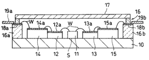
本発明の実施形態について、GaAsFETを用いた半導体装置を例にとり図1を参照して説明する。 An embodiment of the present invention will be described with reference to FIG. 1, taking a semiconductor device using a GaAsFET as an example.
金属製ベース基板10上に電力増幅用などの半導体素子11、たとえばGaAsFETが配置されている。半導体素子11の図示左側に位置する入力側に第1誘電体基板12が配置され、半導体素子11の図示右側に位置する出力側に、第2誘電体基板13が配置されている。第1誘電体基板12上には、たとえば入力側整合回路などを構成する回路パターン12aが形成され、第2誘電体基板13上には、たとえば出力側整合回路などを構成する回路パターン13aが形成されている。第1誘電体基板12の図示左側には、第1誘電体基板12よりも厚い第3誘電体基板14が配置され、第2誘電体基板13の図示右側には、第2誘電体基板13よりも厚い第4誘電体基板15が配置されている。第3誘電体基板14上および第4誘電体基板15上には回路パターン、たとえばマイクロストリップ線路を構成する線路導体14a、15aが形成されている。
A
また、半導体素子11および第1誘電体基板12、第2誘電体基板13、第3誘電体基板14、第4誘電体基板15などを囲んで、ベース基板10上にたとえば矩形枠状の側壁16が所定高さに形成されている。側壁16は、たとえば一部を除いて多くの部分が金属で形成され、また、上部の矩形状開口はたとえば金属製の蓋17で封止されている。
Further, for example, a rectangular frame-
側壁16の図示左側に位置する入力側側壁部分16aおよび側壁16の図示右側に位置する出力側側壁部分16bは絶縁物で形成されている。そして、ベース基板10のたとえば中央領域、たとえば半導体素子11などを配置した領域の平坦な面Sを基準にして、線路導体14aや線路導体15aよりも高い位置で、入力用帯状導体18aおよび出力用帯状導体18bがそれぞれ、入力側側壁部分16aおよび出力側側壁部分16bを貫通している。入力用帯状導体18aには入力用リード線19aが接続され、出力用帯状導体18bには出力用リード線19bが接続されている。
The input
また、入力用帯状導体18aと線路導体14aとの間、および、線路導体14aと回路パターン12aとの間、回路パターン12aと半導体素子11との間、半導体素子11と回路パターン13aとの間、回路パターン13aと線路導体15bとの間、線路導体15bと出力用帯状導体18bとの間は、それぞれワイヤーWで接続されている。
Also, between the
上記した構成において、入力用帯状導体18aから入力する入力信号は、線路導体14aおよび回路パターン12aなどを経て半導体素子11で増幅される。増幅された入力信号は、回路パターン13aおよび線路導体15b、出力用帯状導体18bなどを経て出力される。
In the above configuration, an input signal input from the input strip-
上記した構成によれば、第1誘電体基板12と入力側側壁部分16aとの間に第3誘電体基板14を配置している。また、第2誘電体基板12と出力側側壁部分16bとの間に第4誘電体基板15を配置している。そして、ベース基板10の面Sを基準にして、第3誘電体基板14上の線路導体14aの高さが、第1誘電体基板12上の第1回路パターン12aよりも高く、側壁16を貫通する帯状導体18aよりも低くなっている。同様に、第4誘電体基板15上の線路導体15aの高さが、第2誘電体基板13上の第2回路パターン13aよりも高く、側壁16を貫通する帯状導体18bよりも低くなっている。
According to the configuration described above, the third
したがって、高い電流溶断容量を得るために帯状導体18a、18bの幅を広げ、帯状導体18a、18bとベース基板10間の側壁16を厚くし、帯状導体18a、18bの貫通部分の高さが高くなっても、ワイヤーで接続する回路間の高低差が小さくなる。その結果、ワイヤーで接続する回路間のインピーダンス変化が抑えられ、また、放射損の少ない半導体装置が得られる。
Therefore, in order to obtain a high current fusing capacity, the width of the
上記の実施形態は、ワイヤーで接続する回路間の高低差を小さくするために、たとえば第1誘電体基板12と入力側側壁部分16aとの間に1つの誘電体基板14を配置している。しかし、ワイヤーで接続する回路間の高低差をさらに小さくするために、高さの相違する複数の誘電体基板を配置することもできる。
In the embodiment described above, for example, one
次に、本発明の他の実施形態について図2を参照して説明する。本発明の半導体装置は、たとえば半導体素子を中心にして左右が対称の構造になっている。したがって、図2はその出力側部分を抜き出した図で、図1に対応する部分に同じ符号を付し重複する説明を一部省略する。 Next, another embodiment of the present invention will be described with reference to FIG. The semiconductor device of the present invention has, for example, a symmetrical structure with a semiconductor element as the center. Therefore, FIG. 2 is a diagram in which the output side portion is extracted, and the same reference numerals are given to the portions corresponding to FIG.
この実施形態は、第4誘電体基板15と帯状導体18bとの間に、ベース基板10の面Sを基準にして、その表面が帯状導体18bの高さと同じになる厚さの誘電体基板21を配置し、その表面に線路導体21aを設けている。
In this embodiment, a
たとえば帯状導体18bが側壁16を貫通する部分の近傍、たとえば側壁16の外側や内側、あるいは貫通部分では、側壁16の有無など帯状導体18b周辺の構造が相違している。そのため、インピーダンスが変化しやすく、安定した信号の伝送が困難になっている。
For example, the structure around the belt-
図2の構成によれば、たとえば帯状導体18bと同じ高さに線路導体21aを設けた誘電体基板21を帯状導体18bに隣接して配置している。したがって、インピーダンスが変化しやすい帯状導体18bの近傍では、ワイヤーで接続する回路間の高低差がなくなり、伝送する信号の乱れを小さくできる。
According to the configuration of FIG. 2, for example, the
次に、本発明の他の実施形態について、出力側部分を抜き出した図3を参照して説明する。図3は、図1に対応する部分に同じ符号を付し重複する説明を一部省略する。 Next, another embodiment of the present invention will be described with reference to FIG. 3 in which an output side portion is extracted. In FIG. 3, parts corresponding to those in FIG.
この実施形態は、第2誘電体基板13上に設けた回路パターン13aと帯状導体18bとの間、たとえば第2誘電体基板13上の端部に絶縁ブロック31を配置している。絶縁ブロック31には、貫通穴を設けたVIAホール31aが形成され、また、VIAホール31aを囲むその側面などに導電層31bが形成されている。また、絶縁ブロック31の図示上面に、VIAホール31aに接続する導電パターン31cが形成され、この導電パターン31cと帯状導体18bとの間がワイヤーWで接続されている。
In this embodiment, an insulating
絶縁ブロック31の高さは、たとえば導電パターン31cと帯状導体18bとの間に高低差がないように、帯状導体18bの貫通部分と同じにしている。しかし、絶縁ブロック31の高さを低くし、導電パターン31cの位置を帯状導体18bの貫通部分よりも低くすることもできる。
The height of the insulating
上記した構成によれば、帯状導体18bおよび回路パターン13a間を絶縁ブロック31に設けたVIAホール31aで接続し、VIAホール31aを囲んで導電層31bを形成している。したがって、VIAホール31a部分での放射損を少なくできる。また、VIAホール31aの形状、たとえば貫通穴の径などを変えることにより、VIAホール31a部分のインピーダンスを適宜調整することもできる。
According to the configuration described above, the
次に、本発明の他の実施形態について、出力側部分を抜き出した図4を参照して説明する。図4は、図1に対応する部分に同じ符号を付し重複する説明を一部省略する。 Next, another embodiment of the present invention will be described with reference to FIG. 4 in which an output side portion is extracted. 4, parts corresponding to those in FIG. 1 are denoted by the same reference numerals, and redundant description is partially omitted.
この実施形態は、ベース基板10周辺のたとえばその一部に、中央領域の面Sよりも低い段差面41を設けている。そして、段差面41上に側壁16を形成し、たとえば回路パターン13aと帯状導体18bの高さを同じにしている。
In this embodiment, a
この構成の場合も、段差面41上に側壁16を形成することによって、ワイヤーWで接続する回路間の高低差を小さくでき、上記した実施形態と同様の効果が得られる。
Also in this configuration, by forming the
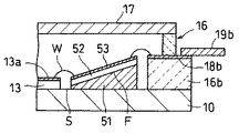
次に、本発明の他の実施形態について、出力側部分を抜き出した図5を参照して説明する。図5は、図1に対応する部分に同じ符号を付し重複する説明を一部省略する。 Next, another embodiment of the present invention will be described with reference to FIG. 5 in which an output side portion is extracted. In FIG. 5, parts corresponding to those in FIG.
この実施形態は、第2誘電体基板13と帯状導体18bとの間のベース基板10上に、ベース基板10の面Sを基準にして、第2誘電体基板13側が低く帯状導体18b側が高くなる傾斜面Fを有する金属ブロック51を設け、この金属ブロック51の傾斜面Fに第2誘電体基板52を設け、さらに第2誘電体基板52上に第2回路パターン53、たとえば線路導体を形成している。
In this embodiment, on the
上記した構成の場合も、金属ブロック51上に形成した回路パターン53が帯状導体18b側から第2誘電体基板13に向かって徐々に低くなっている。そのため、ワイヤーWで接続する回路間の高低差が小さくなり、上記した実施形態と同様の効果が得られる。
Also in the case of the configuration described above, the
金属ブロック51はベース基板10の表面を加工して形成してよく、別に形成した金属ブロック51をベース基板10上に接合してもよい。
The
次に、本発明の他の実施形態について、出力側部分を抜き出した図6を参照して説明する。図6は、図1に対応する部分に同じ符号を付し重複する説明を一部省略する。 Next, another embodiment of the present invention will be described with reference to FIG. 6 in which an output side portion is extracted. In FIG. 6, parts corresponding to those in FIG.
この実施形態は、第2誘電体基板13と帯状導体18bとの間のベース基板10上に、ベース基板10の面Sを基準にして、第2誘電体基板13側が低く、帯状導体18b側が高くなる傾斜面Gを有する絶縁ブロック61を配置している。そして、絶縁ブロック61の傾斜面Gに回路パターン62、たとえば線路導体を形成している。
In this embodiment, on the
この場合も、ワイヤーWで接続する回路間の高低差が小さくなり、上記した実施形態と同様の効果が得られる。 Also in this case, the height difference between the circuits connected by the wire W is reduced, and the same effect as the above-described embodiment can be obtained.
10…ベース基板
11…半導体素子
12…第1誘電体基板
12a…回路パターン
13…第2誘電体基板
13a…回路パターン
14…第3誘電体基板
14a…線路導体
15…第4誘電体基板
15a…線路導体
16…側壁
17…蓋
18a…入力用帯状導体
18b…出力用帯状導体
19a…入力用リード線
19b…出力用リード線
S…ベース基板の面
DESCRIPTION OF
Claims (1)
Priority Applications (1)
| Application Number | Priority Date | Filing Date | Title |
|---|---|---|---|
| JP2011253655A JP5259807B2 (en) | 2011-11-21 | 2011-11-21 | Semiconductor device |
Applications Claiming Priority (1)
| Application Number | Priority Date | Filing Date | Title |
|---|---|---|---|
| JP2011253655A JP5259807B2 (en) | 2011-11-21 | 2011-11-21 | Semiconductor device |
Related Parent Applications (1)
| Application Number | Title | Priority Date | Filing Date |
|---|---|---|---|
| JP2010086000A Division JP5135376B2 (en) | 2010-04-02 | 2010-04-02 | Semiconductor device |
Publications (2)
| Publication Number | Publication Date |
|---|---|
| JP2012039160A JP2012039160A (en) | 2012-02-23 |
| JP5259807B2 true JP5259807B2 (en) | 2013-08-07 |
Family
ID=45850714
Family Applications (1)
| Application Number | Title | Priority Date | Filing Date |
|---|---|---|---|
| JP2011253655A Expired - Fee Related JP5259807B2 (en) | 2011-11-21 | 2011-11-21 | Semiconductor device |
Country Status (1)
| Country | Link |
|---|---|
| JP (1) | JP5259807B2 (en) |
Families Citing this family (1)
| Publication number | Priority date | Publication date | Assignee | Title |
|---|---|---|---|---|
| CN114362841B (en) * | 2021-12-13 | 2023-12-15 | 深圳市卓汉材料技术有限公司 | A passive intermodulation test fixture and a passive intermodulation test system |
Family Cites Families (4)
| Publication number | Priority date | Publication date | Assignee | Title |
|---|---|---|---|---|
| JPS6114181Y2 (en) * | 1981-02-25 | 1986-05-02 | ||
| JPS6114183Y2 (en) * | 1981-02-25 | 1986-05-02 | ||
| JPH0770641B2 (en) * | 1989-03-17 | 1995-07-31 | 三菱電機株式会社 | Semiconductor package |
| JP3735270B2 (en) * | 2001-05-11 | 2006-01-18 | 松下電器産業株式会社 | High frequency semiconductor device |
-
2011
- 2011-11-21 JP JP2011253655A patent/JP5259807B2/en not_active Expired - Fee Related
Also Published As
| Publication number | Publication date |
|---|---|
| JP2012039160A (en) | 2012-02-23 |
Similar Documents
| Publication | Publication Date | Title |
|---|---|---|
| JP4519637B2 (en) | Semiconductor device | |
| US9978691B2 (en) | Semiconductor packages having wire bond wall to reduce coupling | |
| US9401342B2 (en) | Semiconductor package having wire bond wall to reduce coupling | |
| EP2515435B1 (en) | Power amplifier | |
| JP6273247B2 (en) | High frequency semiconductor amplifier | |
| CN107851635B (en) | Conductive seal ring for power distribution | |
| JP5259807B2 (en) | Semiconductor device | |
| JP6849060B2 (en) | amplifier | |
| CN104113289B (en) | A kind of microwave integrated amplifier circuit and preparation method thereof | |
| JP5135376B2 (en) | Semiconductor device | |
| JP2012039159A (en) | Semiconductor device | |
| JPWO2007108262A1 (en) | Transceiver | |
| US20140132353A1 (en) | Amplifier circuit | |
| CN114420657B (en) | Semiconductor device and preparation method of semiconductor device | |
| JP2015173234A (en) | Package for high-frequency semiconductor device, manufacturing method thereof and high-frequency semiconductor device | |
| JP5162826B2 (en) | Semiconductor device and manufacturing method thereof | |
| CN104465616A (en) | Reliability analysis testing structure and method of integrated circuit | |
| CN106876440A (en) | Reduce substrat structure of SOI substrate capacity effect and preparation method thereof | |
| US11038031B2 (en) | Field-effect transistor | |
| JP5564763B2 (en) | Method for manufacturing MOS type semiconductor device | |
| CN107039356A (en) | Micron waveband and millimere-wave band packaging body | |
| CN108109913A (en) | The production method of bipolar transistor | |
| JP2005072954A (en) | High frequency circuit equipment | |
| KR20040081173A (en) | Device for connecting an ic terminal to a reference potential | |
| CN121772253A (en) | Semiconductor device, manufacturing method thereof, power amplifier and electronic equipment |
Legal Events
| Date | Code | Title | Description |
|---|---|---|---|
| A621 | Written request for application examination |
Free format text: JAPANESE INTERMEDIATE CODE: A621 Effective date: 20111121 |
|
| A977 | Report on retrieval |
Free format text: JAPANESE INTERMEDIATE CODE: A971007 Effective date: 20130118 |
|
| A131 | Notification of reasons for refusal |
Free format text: JAPANESE INTERMEDIATE CODE: A131 Effective date: 20130122 |
|
| A521 | Request for written amendment filed |
Free format text: JAPANESE INTERMEDIATE CODE: A523 Effective date: 20130307 |
|
| TRDD | Decision of grant or rejection written | ||
| A01 | Written decision to grant a patent or to grant a registration (utility model) |
Free format text: JAPANESE INTERMEDIATE CODE: A01 Effective date: 20130402 |
|
| A61 | First payment of annual fees (during grant procedure) |
Free format text: JAPANESE INTERMEDIATE CODE: A61 Effective date: 20130424 |
|
| FPAY | Renewal fee payment (event date is renewal date of database) |
Free format text: PAYMENT UNTIL: 20160502 Year of fee payment: 3 |
|
| LAPS | Cancellation because of no payment of annual fees |