JP5225733B2 - Grinding equipment - Google Patents
Grinding equipment Download PDFInfo
- Publication number
- JP5225733B2 JP5225733B2 JP2008108867A JP2008108867A JP5225733B2 JP 5225733 B2 JP5225733 B2 JP 5225733B2 JP 2008108867 A JP2008108867 A JP 2008108867A JP 2008108867 A JP2008108867 A JP 2008108867A JP 5225733 B2 JP5225733 B2 JP 5225733B2
- Authority
- JP
- Japan
- Prior art keywords
- wafer
- chuck table
- grinding
- holding
- unit
- Prior art date
- Legal status (The legal status is an assumption and is not a legal conclusion. Google has not performed a legal analysis and makes no representation as to the accuracy of the status listed.)
- Active
Links
Images
Landscapes
- Grinding Of Cylindrical And Plane Surfaces (AREA)
- Grinding-Machine Dressing And Accessory Apparatuses (AREA)
- Mechanical Treatment Of Semiconductor (AREA)
Description
本発明は、研削装置及び該研削装置を使用したウエーハの研削方法に関する。 The present invention relates to a grinding apparatus and a wafer grinding method using the grinding apparatus.
IC、LSI等の数多くのデバイスが表面に形成され、且つ個々のデバイスが分割予定ライン(ストリート)によって区画された半導体ウエーハは、研削装置によって裏面が研削されて所定の厚みに加工された後、ダイシング装置によって分割予定ラインを切削して個々のデバイスに分割され、携帯電話、パソコン等の電気機器に利用される。 A semiconductor wafer in which a number of devices such as IC and LSI are formed on the surface, and each device is partitioned by a line to be divided (street), the back surface is ground by a grinding machine and processed to a predetermined thickness. The division line is cut by a dicing machine and divided into individual devices, which are used for electric devices such as mobile phones and personal computers.
研削装置は、ウエーハを保持する保持面を有するチャックテーブルと、該チャックテーブルの保持面に保持されたウエーハを研削する研削ホイールが回転可能に装着された研削手段と、該チャックテーブルにウエーハを搬送する搬送手段から概ね構成されており、ウエーハを効率良く所定の厚さに研削することができる。
研削装置によるウエーハの研削時に、チャックテーブルとウエーハとの間に研削屑又は研削ホイールから脱落した砥粒等の異物が介在したまま研削すると、異物の出っ張りがウエーハの研削面に現れて局部的に研削され、研削済みのウエーハに窪み(ディンプル)が生じるという問題がある。 When grinding a wafer with a grinding device, if the foreign material such as grinding debris or abrasive grains dropped from the grinding wheel is interposed between the chuck table and the wafer, the protrusion of the foreign material appears on the ground surface of the wafer and is locally There is a problem that a dimple is generated in the ground and ground wafer.
特に、シリコンインゴットから切り出したウエーハの切断面を研削してベアウエーハを形成する場合には、研削済みの表面にディンプルが生じると致命的な欠陥となる。 In particular, when a bare wafer is formed by grinding a cut surface of a wafer cut out from a silicon ingot, if dimples are generated on the ground surface, a fatal defect occurs.
本発明はこのような点に鑑みてなされたものであり、その目的とするところは、ウエーハの研削面にディンプルが生じることのない研削装置及びウエーハの研削方法を提供することである。 The present invention has been made in view of these points, and an object of the present invention is to provide a grinding apparatus and a wafer grinding method in which dimples are not generated on the grinding surface of the wafer.
本発明によると、ウエーハを保持する保持面を有するチャックテーブルと、該チャックテーブルの保持面に保持されたウエーハを研削する研削ホイールが回転可能に装着された研削手段と、ウエーハを吸引保持するウエーハ保持部と該ウエーハ保持部を移送する移送部とから構成され該チャックテーブルにウエーハを搬送する搬送手段とを備えた研削装置であって、該チャックテーブルの側面に配設された細長い水噴出口を有するノズルを更に具備し、該搬送手段によってウエーハを該チャックテーブルに搬送する際、該搬送手段の保持部に保持されたウエーハと該チャックテーブルの保持面との間に隙間を形成し、該隙間に該ノズルの該水噴出口から洗浄水を噴出してウエーハのチャックテーブル対向面とチャックテーブルの保持面とを洗浄することを特徴とする研削装置が提供される。 According to the present invention, a chuck table having a holding surface for holding a wafer, a grinding means on which a grinding wheel for grinding the wafer held on the holding surface of the chuck table is rotatably mounted, and a wafer for sucking and holding the wafer. An elongate water jetting outlet disposed on a side surface of the chuck table, comprising a holding unit and a transfer unit configured to transfer the wafer holding unit, and comprising a conveying means for conveying the wafer to the chuck table. And when the wafer is conveyed to the chuck table by the conveying means, a gap is formed between the wafer held by the holding portion of the conveying means and the holding surface of the chuck table, wash the chuck table facing surface of the wafer by ejecting the washing water from the aqueous spout of the nozzle to the gap and the holding surface of the chuck table Grinding apparatus is provided which is characterized in that.
本発明の研削装置によると、搬送手段によってウエーハをチャックテーブルに搬送する際、搬送手段の保持部に保持されたウエーハとチャックテーブルの保持面との間に隙間を形成し、その隙間に洗浄水を供給してウエーハのチャックテーブル対向面とチャックテーブルの保持面とを洗浄する細長い水噴出口を有するノズルが配設されているので、チャックテーブルの保持面及び/又はウエーハのチャックテーブル対向面に異物があっても洗い流され、ウエーハの研削面にディンプルが生じることがない。 According to the grinding apparatus of the present invention, when the wafer is transferred to the chuck table by the transfer means, a gap is formed between the wafer held by the holding portion of the transfer means and the holding surface of the chuck table, and the cleaning water is formed in the gap. Is provided with an elongated water jet outlet for cleaning the wafer chuck table facing surface and the chuck table holding surface, so that the chuck table holding surface and / or the wafer chuck table facing surface is disposed. Even if there is a foreign object, it is washed away and dimples are not generated on the ground surface of the wafer.
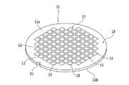
以下、本発明実施形態のウエーハの研削方法及び研削装置を図面を参照して詳細に説明する。図1は所定の厚さに加工される前の半導体ウエーハの斜視図である。図1に示す半導体ウエーハ11は、例えば厚さが700μmのシリコンウエーハからなっており、表面11aに複数のストリート13が格子状に形成されているとともに、該複数のストリート13によって区画された複数の領域にIC,LSI等のデバイス15が形成されている。
Hereinafter, a wafer grinding method and a grinding apparatus according to embodiments of the present invention will be described in detail with reference to the drawings. FIG. 1 is a perspective view of a semiconductor wafer before being processed to a predetermined thickness. A
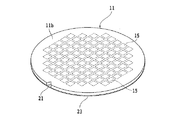
このように構成された半導体ウエーハ11は、デバイス15が形成されているデバイス領域17と、デバイス領域17を囲繞する外周余剰領域19を備えている。また、半導体ウエーハ11の外周には、シリコンウエーハの結晶方位を示すマークとしてのノッチ21が形成されている。
The
半導体ウエーハ11の表面11aには、保護テープ貼着工程により保護テープ23が貼着される。従って、半導体ウエーハ11の表面11aは保護テープ23によって保護され、図2に示すように裏面11bが露出する形態となる。
A
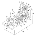
以下、このように構成された半導体ウエーハ11の裏面11bを所定厚さに研削する研削装置2を図3を参照して説明する。研削装置2のハウジング4は、水平ハウジング部分6と、垂直ハウジング部分8から構成される。
Hereinafter, a
垂直ハウジング部分8には上下方向に伸びる1対のガイドレール12,14が固定されている。この一対のガイドレール12,14に沿って研削手段(研削ユニット)16が上下方向に移動可能に装着されている。研削ユニット16は支持部20を介して一対のガイドレール12,14に沿って上下方向に移動する移動基台18に取り付けられている。
A pair of
研削ユニット16は、支持部20に取り付けられたスピンドルハウジング22と、スピンドルハウジング22中に回転可能に収容されたスピンドル24と、スピンドル24を回転駆動するサーボモータ26を含んでいる。
The
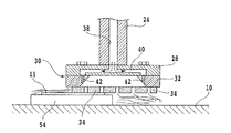
図6に最も良く示されるように、スピンドル24の先端部にはマウンター28が固定されており、このマウンター28には研削ホイール30がねじ止めされている。例えば、研削ホイール30はホイール基台32の自由端部に粒径0.3〜1.0μmのダイヤモンド砥粒をビトリファイドボンドで固めた複数の研削砥石34が固着されて構成されている。
As best shown in FIG. 6, a
研削手段(研削ユニット)16にはホース36を介して研削水が供給される。好ましくは、研削水としては純水が使用される。図6に示すように、ホース36から供給された研削水が、スピンドル24に形成された研削水供給穴38、マウンター28に形成された空間40及び研削ホイール30のホイール基台32に形成された複数の研削水供給ノズル42を介して研削砥石34及びチャックテーブル54に保持されたウエーハ11に供給される。
Grinding water is supplied to the grinding means (grinding unit) 16 via a
図3を再び参照すると、研削装置2は、研削ユニット16を一対の案内レール12,14に沿って上下方向に移動する研削ユニット送り機構44を備えている。研削ユニット送り機構44は、ボールねじ46と、ボールねじ46の一端部に固定されたパルスモータ48から構成される。パルスモータ48をパルス駆動すると、ボールねじ46が回転し、移動基台18の内部に固定されたボールねじ46のナットを介して移動基台18が上下方向に移動される。
Referring back to FIG. 3, the
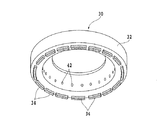
水平ハウジング部分6の凹部10には、チャックテーブルユニット50が配設されている。チャックテーブルユニット50は、図4に示すように、支持基台52と、支持基台52に回転自在に配設されたチャックテーブル54を含んでいる。チャックテーブルユニット50は更に、チャックテーブル54を挿通する穴を有したカバー56を備えている。
A
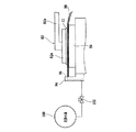
カバー56の側面には、細長い水噴出口96を有するノズル(洗浄手段)94が配設されている。ノズル94は、図7に示すように開閉弁102を介して洗浄水源100に接続されている。
On the side surface of the
チャックテーブルユニット50は、チャックテーブル移動機構58により研削装置2の前後方向に移動される。チャックテーブル移動機構58は、ボールねじ60と、ボールねじ60のねじ軸62の一端に連結されたパルスモータ64から構成される。
The
パルスモータ64をパルス駆動すると、ボールねじ60のねじ軸62が回転し、このねじ軸62に螺合したナットを有する支持基台52が研削装置2の前後方向に移動する。よって、チャックテーブル54もパルスモータ64の回転方向に応じて、前後方向に移動する。
When the
図3に示されているように、図4に示した一対のガイドレール66,68及びチャックテーブル移動機構58は蛇腹70,72により覆われている。すなわち、蛇腹70の前端部は凹部10を画成する前壁に固定され、後端部がカバー56の前端面に固定されている。また、蛇腹72の後端は垂直ハウジング部分8に固定され、その前端はカバー56の後端面に固定されている。
As shown in FIG. 3, the pair of guide rails 66 and 68 and the chuck
ハウジング4の水平ハウジング部分6には、第1のウエーハカセット74と、第2のウエーハカセット76と、ウエーハ搬送手段78と、ウエーハ仮載置手段80と、ウエーハ搬入手段82と、ウエーハ搬出手段84と、洗浄手段86が配設されている。
In the horizontal housing portion 6 of the housing 4, a
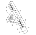
更に、ハウジング4の前方にはオペレータが研削条件等を入力する操作手段88が設けられている。ウエーハ搬入手段82は、ウエーハを吸引保持するウエーハ保持部82aと、ウエーハ保持部82aを移送する移送部(アーム)82bから構成されている。
Further, an operation means 88 is provided in front of the housing 4 for an operator to input grinding conditions and the like. The wafer carry-in
また、水平ハウジング部分6の概略中央部には、チャックテーブル54を洗浄する洗浄水噴射ノズル90が設けられている。この洗浄水噴射ノズル90は、チャックテーブルユニット54がウエーハ搬入・搬出領域に位置づけられた状態において、チャックテーブル54に保持された研削加工後のウエーハに向けて洗浄水を噴出する。
Further, a cleaning
チャックテーブルユニット50は、チャックテーブル移動機構58のパルスモータ64をパルス駆動することにより、図3に示した装置奥側の研削領域と、ウエーハ搬入手段82からウエーハを受け取りウエーハ搬出手段84にウエーハを受け渡す手前側のウエーハ搬入・搬出領域との間で移動される。
The
このように構成された研削装置2の研削作業について以下に説明する。第1のウエーハカセット74中に収容されるウエーハは、保護テープが表面側(回路が形成されている側の面)に装着された半導体ウエーハであり、従ってウエーハは裏面が上側に位置する状態で第1のカセット74中に収容されている。このように複数の半導体ウエーハを収容した第1のウエーハカセット74は、ハウジング4の所定のカセットを搬入領域に載置される。
The grinding operation of the
そして、カセット搬入領域に載置された第1のウエーハカセット74に収容されていた研削加工前の半導体ウエーハが全て搬出されると、空のウエーハカセット74に変えて複数個の半導体ウエーハを収容した新しい第1のウエーハカセット74が手動でカセット搬入領域に載置される。
When all of the unprocessed semiconductor wafers contained in the
一方、ハウジング4の所定のカセット搬出領域に載置された第2のウエーハカセット76に所定枚数の研削加工後の半導体ウエーハが搬入されると、かかる第2のウエーハカセット76は手動で搬出されて、新しい空の第2のウエーハカセット76がカセット搬出領域に載置される。
On the other hand, when a predetermined number of ground semiconductor wafers are loaded into the
第1のウエーハカセット74に収容された半導体ウエーハは、ウエーハ搬送手段78の上下動作及び進退動作により搬送され、ウエーハ仮載置手段80に載置される。ウエーハ仮載置手段80に載置されたウエーハは、ここで中心合わせが行われた後にウエーハ搬入手段82の旋回動作によって、ウエーハ搬入・搬出領域に位置せしめられているチャックテーブルユニット50のチャックテーブル54に載置され、チャックテーブル54によって吸引保持される。
The semiconductor wafer accommodated in the
ウエーハがウエーハ搬入手段82の旋回動作によってチャックテーブル54上に載置される前に、図7に示すようにウエーハ搬入手段82のウエーハ保持部82aに保持されたウエーハ11とチャックテーブル54の保持面との間に例えば1mm〜5mm程度の僅かな隙間を形成する。
Before the wafer is placed on the chuck table 54 by the turning operation of the wafer carry-in means 82, the
そして、開閉弁102を開いてノズル94の水噴出口96から洗浄水98をウエーハ11とチャックテーブル54の保持面の間に噴出する。これにより、チャックテーブルの保持面及び/又はウエーハのチャックテーブル対向面に異物があっても洗浄水98により洗い流され、その後の研削作業によってウエーハの研削面にディンプルが生じることがない。
Then, the on-off
このようにチャックテーブル54がウエーハを吸引保持したならば、チャックテーブル移動機構58を作動して、チャックテーブルユニット54を移動して装置後方の研削領域に位置づける。
When the chuck table 54 sucks and holds the wafer in this way, the chuck
チャックテーブルユニット50が研削領域に位置づけられると、チャックテーブル54に保持されたウエーハの中心が研削ホイール30の外周円を僅かに超えた位置に位置づけられる。
When the
次に、チャックテーブル54を例えば100〜300rpm程度で回転し、サーボモータ26を駆動して研削ホイール30を4000〜7000rpmで回転するとともに、研削ユニット送り機構44のパルスモータ48を正転駆動して研削ユニット16を下降させる。
Next, the chuck table 54 is rotated at, for example, about 100 to 300 rpm, the
そして、図6に示すように、研削ホイール30の研削砥石34をチャックテーブル54上のウエーハ11の裏面(被研削面)に所定の荷重で押圧することにより、ウエーハ11の裏面が研削される。このようにして所定時間研削することにより、ウエーハ11が所定の厚さに研削される。
Then, as shown in FIG. 6, the back surface of the
研削が終了すると、チャックテーブル移動機構58を駆動してチャックテーブル54を装置手前側のウエーハ搬入・搬出領域に位置付ける。チャックテーブル54がウエーハ搬入・搬出領域に位置付けられたならば、洗浄水噴射ノズル90から洗浄水を噴射して、チャックテーブル54に保持されている研削加工されたウエーハ11の被研削面(裏面)を洗浄する。
When grinding is completed, the chuck
洗浄水噴射ノズル90でウエーハ11の裏面を洗浄後、チャックテーブル54に保持されているウエーハの吸引保持が解除されてから、ウエーハはウエーハ搬出手段84により洗浄手段86に搬送される。
After cleaning the back surface of the
洗浄手段86に搬送されたウエーハは、ここで洗浄されるとともにスピン乾燥される。次いで、ウエーハがウエーハ搬送手段78により第2のウエーハカセット76の所定位置に収納される。
The wafer conveyed to the cleaning means 86 is cleaned and spin-dried here. Next, the wafer is stored in a predetermined position of the
上述した実施形態の研削装置2で研削するのに適した半導体ウエーハは、図1に示したような複数のデバイス15がその表面に形成されたウエーハ11に限定されるものではない。
The semiconductor wafer suitable for grinding by the grinding
半導体形成プロセスの前工程であるフォトリソグラフィによりウエーハ上に回路を形成する前のベアウエーハにディンプル(窪み)が生じると致命的な欠陥となるため、研削装置2はシリコンインゴットから切り出したウエーハの切断面を研削してベアウエーハを形成する応用例に特に適している。
If dimples (dents) occur in a bare wafer before forming a circuit on the wafer by photolithography, which is a pre-process of the semiconductor formation process, a fatal defect is generated. Therefore, the grinding
2 研削装置
11 半導体ウエーハ
16 研削手段(研削ユニット)
24 スピンドル
26 サーボモータ
30 研削ホイール
34 研削砥石
50 チャックテーブルユニット
54 チャックテーブル
82 ウエーハ搬入手段
94 洗浄手段(ノズル)
96 水噴出口
2 Grinding
24
96 Water spout
Claims (2)
該チャックテーブルの側面に配設された細長い水噴出口を有するノズルを更に具備し、
該搬送手段によってウエーハを該チャックテーブルに搬送する際、該搬送手段の保持部に保持されたウエーハと該チャックテーブルの保持面との間に隙間を形成し、該隙間に該ノズルの該水噴出口から洗浄水を噴出してウエーハのチャックテーブル対向面とチャックテーブルの保持面とを洗浄することを特徴とする研削装置。 A chuck table having a holding surface for holding a wafer, a grinding means on which a grinding wheel for grinding a wafer held on the holding surface of the chuck table is rotatably mounted, a wafer holding unit for sucking and holding a wafer, and the wafer A grinding device comprising a transfer unit configured to transfer a holding unit and a transfer unit configured to transfer a wafer to the chuck table,
Further comprising a nozzle having an elongated water jet disposed on a side surface of the chuck table;
When the wafer is transferred to the chuck table by the transfer means, a gap is formed between the wafer held by the holding portion of the transfer means and the holding surface of the chuck table, and the water jet of the nozzle is inserted into the gap. A grinding apparatus for cleaning a wafer facing a chuck table and a chuck table holding surface by jetting cleaning water from an outlet .
Priority Applications (1)
| Application Number | Priority Date | Filing Date | Title |
|---|---|---|---|
| JP2008108867A JP5225733B2 (en) | 2008-04-18 | 2008-04-18 | Grinding equipment |
Applications Claiming Priority (1)
| Application Number | Priority Date | Filing Date | Title |
|---|---|---|---|
| JP2008108867A JP5225733B2 (en) | 2008-04-18 | 2008-04-18 | Grinding equipment |
Publications (2)
| Publication Number | Publication Date |
|---|---|
| JP2009255247A JP2009255247A (en) | 2009-11-05 |
| JP5225733B2 true JP5225733B2 (en) | 2013-07-03 |
Family
ID=41383339
Family Applications (1)
| Application Number | Title | Priority Date | Filing Date |
|---|---|---|---|
| JP2008108867A Active JP5225733B2 (en) | 2008-04-18 | 2008-04-18 | Grinding equipment |
Country Status (1)
| Country | Link |
|---|---|
| JP (1) | JP5225733B2 (en) |
Families Citing this family (4)
| Publication number | Priority date | Publication date | Assignee | Title |
|---|---|---|---|---|
| JP6025325B2 (en) * | 2011-12-19 | 2016-11-16 | 株式会社東京精密 | Wafer grinding method |
| JP6316702B2 (en) * | 2014-08-08 | 2018-04-25 | 株式会社ディスコ | Processing apparatus and wafer processing method |
| JP2016127195A (en) * | 2015-01-07 | 2016-07-11 | 株式会社ディスコ | Wafer grinding method |
| JP6726591B2 (en) * | 2016-09-30 | 2020-07-22 | 株式会社ディスコ | Processing equipment |
Family Cites Families (5)
| Publication number | Priority date | Publication date | Assignee | Title |
|---|---|---|---|---|
| JP4009367B2 (en) * | 1998-08-04 | 2007-11-14 | 株式会社ディスコ | Spin cleaning / drying method |
| JP4385390B2 (en) * | 1998-10-29 | 2009-12-16 | 株式会社東京精密 | Wafer chamfering equipment |
| JP2004090128A (en) * | 2002-08-30 | 2004-03-25 | Nippei Toyama Corp | Semiconductor wafer grinding machine |
| JP4963411B2 (en) * | 2005-12-21 | 2012-06-27 | ルネサスエレクトロニクス株式会社 | Manufacturing method of semiconductor device or semiconductor wafer |
| JP4906445B2 (en) * | 2006-09-01 | 2012-03-28 | 株式会社ディスコ | Wafer processing method |
-
2008
- 2008-04-18 JP JP2008108867A patent/JP5225733B2/en active Active
Also Published As
| Publication number | Publication date |
|---|---|
| JP2009255247A (en) | 2009-11-05 |
Similar Documents
| Publication | Publication Date | Title |
|---|---|---|
| JP5275016B2 (en) | Grinding equipment | |
| JP5669518B2 (en) | Wafer transfer mechanism | |
| JP2009125915A (en) | Grinding wheel mounting mechanism | |
| CN110340800B (en) | Grinding device | |
| JP2009061511A (en) | Wafer grinding method and grinding apparatus | |
| JP5455609B2 (en) | Grinding apparatus and wafer grinding method using the grinding apparatus | |
| JP5225733B2 (en) | Grinding equipment | |
| JP2009113145A (en) | Polishing machine chuck table mechanism | |
| JP5345457B2 (en) | Grinding equipment | |
| JP4733943B2 (en) | Polishing pad dressing method | |
| JP5837367B2 (en) | Grinding equipment | |
| JP2009135254A (en) | Adhesive tape application method | |
| JP5037255B2 (en) | Grinding apparatus and observation method of grinding apparatus | |
| JP5700988B2 (en) | Wafer grinding method | |
| CN102343444B (en) | The processing unit (plant) of semiconductor wafer | |
| JP5172457B2 (en) | Grinding apparatus and grinding method | |
| JP5306928B2 (en) | Wafer transfer device | |
| JP5875224B2 (en) | Grinding equipment | |
| JP5160190B2 (en) | Grinding apparatus and grinding method | |
| JP5399829B2 (en) | Polishing pad dressing method | |
| JP3401706B2 (en) | Surface grinding equipment | |
| JP7452960B2 (en) | processing equipment | |
| JP2011146568A (en) | Method and device for detecting cracking of wafer | |
| CN114536127A (en) | Grinding device | |
| JP2010046763A (en) | Grinding device |
Legal Events
| Date | Code | Title | Description |
|---|---|---|---|
| A621 | Written request for application examination |
Free format text: JAPANESE INTERMEDIATE CODE: A621 Effective date: 20110322 |
|
| A977 | Report on retrieval |
Free format text: JAPANESE INTERMEDIATE CODE: A971007 Effective date: 20121119 |
|
| A131 | Notification of reasons for refusal |
Free format text: JAPANESE INTERMEDIATE CODE: A131 Effective date: 20121211 |
|
| A521 | Request for written amendment filed |
Free format text: JAPANESE INTERMEDIATE CODE: A523 Effective date: 20130204 |
|
| TRDD | Decision of grant or rejection written | ||
| A01 | Written decision to grant a patent or to grant a registration (utility model) |
Free format text: JAPANESE INTERMEDIATE CODE: A01 Effective date: 20130312 |
|
| A61 | First payment of annual fees (during grant procedure) |
Free format text: JAPANESE INTERMEDIATE CODE: A61 Effective date: 20130313 |
|
| R150 | Certificate of patent or registration of utility model |
Free format text: JAPANESE INTERMEDIATE CODE: R150 Ref document number: 5225733 Country of ref document: JP Free format text: JAPANESE INTERMEDIATE CODE: R150 |
|
| FPAY | Renewal fee payment (event date is renewal date of database) |
Free format text: PAYMENT UNTIL: 20160322 Year of fee payment: 3 |
|
| R250 | Receipt of annual fees |
Free format text: JAPANESE INTERMEDIATE CODE: R250 |
|
| R250 | Receipt of annual fees |
Free format text: JAPANESE INTERMEDIATE CODE: R250 |
|
| R250 | Receipt of annual fees |
Free format text: JAPANESE INTERMEDIATE CODE: R250 |
|
| R250 | Receipt of annual fees |
Free format text: JAPANESE INTERMEDIATE CODE: R250 |
|
| R250 | Receipt of annual fees |
Free format text: JAPANESE INTERMEDIATE CODE: R250 |
|
| R250 | Receipt of annual fees |
Free format text: JAPANESE INTERMEDIATE CODE: R250 |
|
| R250 | Receipt of annual fees |
Free format text: JAPANESE INTERMEDIATE CODE: R250 |
|
| R250 | Receipt of annual fees |
Free format text: JAPANESE INTERMEDIATE CODE: R250 |
|
| R250 | Receipt of annual fees |
Free format text: JAPANESE INTERMEDIATE CODE: R250 |
|
| R250 | Receipt of annual fees |
Free format text: JAPANESE INTERMEDIATE CODE: R250 |