JP2009135254A - Method of sticking adhesive tape - Google Patents
Method of sticking adhesive tape Download PDFInfo
- Publication number
- JP2009135254A JP2009135254A JP2007309794A JP2007309794A JP2009135254A JP 2009135254 A JP2009135254 A JP 2009135254A JP 2007309794 A JP2007309794 A JP 2007309794A JP 2007309794 A JP2007309794 A JP 2007309794A JP 2009135254 A JP2009135254 A JP 2009135254A
- Authority
- JP
- Japan
- Prior art keywords
- wafer
- chuck table
- adhesive tape
- grinding
- sheet layer
- Prior art date
- Legal status (The legal status is an assumption and is not a legal conclusion. Google has not performed a legal analysis and makes no representation as to the accuracy of the status listed.)
- Pending
Links
- 239000002390 adhesive tape Substances 0.000 title claims abstract description 32
- 238000000034 method Methods 0.000 title claims abstract description 17
- 239000010410 layer Substances 0.000 claims description 30
- 239000012790 adhesive layer Substances 0.000 claims description 13
- 239000003292 glue Substances 0.000 claims description 6
- 239000004820 Pressure-sensitive adhesive Substances 0.000 claims description 3
- 239000004925 Acrylic resin Substances 0.000 claims description 2
- 229920000178 Acrylic resin Polymers 0.000 claims description 2
- BZHJMEDXRYGGRV-UHFFFAOYSA-N Vinyl chloride Chemical compound ClC=C BZHJMEDXRYGGRV-UHFFFAOYSA-N 0.000 claims description 2
- 239000011248 coating agent Substances 0.000 abstract 2
- 238000000576 coating method Methods 0.000 abstract 2
- 235000012431 wafers Nutrition 0.000 description 127
- 238000005520 cutting process Methods 0.000 description 29
- 230000001681 protective effect Effects 0.000 description 17
- 239000004065 semiconductor Substances 0.000 description 15
- XLYOFNOQVPJJNP-UHFFFAOYSA-N water Substances O XLYOFNOQVPJJNP-UHFFFAOYSA-N 0.000 description 12
- 238000004140 cleaning Methods 0.000 description 11
- 238000003384 imaging method Methods 0.000 description 7
- XUIMIQQOPSSXEZ-UHFFFAOYSA-N Silicon Chemical compound [Si] XUIMIQQOPSSXEZ-UHFFFAOYSA-N 0.000 description 2
- 239000003595 mist Substances 0.000 description 2
- 230000002093 peripheral effect Effects 0.000 description 2
- 229910052710 silicon Inorganic materials 0.000 description 2
- 239000010703 silicon Substances 0.000 description 2
- 239000007921 spray Substances 0.000 description 2
- 238000003860 storage Methods 0.000 description 2
- 239000006061 abrasive grain Substances 0.000 description 1
- 239000000853 adhesive Substances 0.000 description 1
- 230000001070 adhesive effect Effects 0.000 description 1
- 239000013078 crystal Substances 0.000 description 1
- 229910003460 diamond Inorganic materials 0.000 description 1
- 239000010432 diamond Substances 0.000 description 1
- 238000003754 machining Methods 0.000 description 1
- 239000011295 pitch Substances 0.000 description 1
- 238000003825 pressing Methods 0.000 description 1
- 238000005507 spraying Methods 0.000 description 1
Images


Abstract
Description
本発明は、半導体ウエーハに粘着テープを貼着する粘着テープ貼着方法に関する。 The present invention relates to an adhesive tape attaching method for attaching an adhesive tape to a semiconductor wafer.
IC、LSI等の数多くのデバイスが表面に形成され、且つ個々のデバイスが分割予定ライン(ストリート)によって区画された半導体ウエーハは、研削装置によって裏面が研削されて所定の厚みに加工された後、切削装置(ダイシング装置)によって分割予定ラインを切削して個々のデバイスに分割され、携帯電話、パソコン等の電気機器に利用される。 A semiconductor wafer in which a number of devices such as IC and LSI are formed on the surface, and each device is partitioned by a line to be divided (street), the back surface is ground by a grinding machine and processed to a predetermined thickness. A dividing line is cut by a cutting device (dicing device) and divided into individual devices, which are used for electric devices such as mobile phones and personal computers.
ウエーハの裏面を研削する研削装置は、ウエーハを保持するチャックテーブルと、該チャックテーブルに保持されたウエーハを研削する研削砥石を回転可能に支持する研削ユニットから概ね構成され、ウエーハを高精度に所定の厚さに研削することができる。 A grinding apparatus that grinds the back surface of a wafer is generally composed of a chuck table that holds a wafer and a grinding unit that rotatably supports a grinding wheel that grinds the wafer held by the chuck table. Can be ground to thickness.
そして、ウエーハの裏面を研削する際には複数のデバイスが形成されたウエーハの表面をチャックテーブルに対面させて載置することから、デバイスが損傷する恐れがあるためウエーハの表面には粘着テープ(保護テープ)が貼着される。 When the back surface of the wafer is ground, the wafer surface on which a plurality of devices are formed is placed facing the chuck table, so that the device may be damaged. A protective tape is attached.
また、ダイシングフレームに粘着テープ(ダイシングテープ)を介して配設されたウエーハを切削ブレードで切削して所定深さのV溝を形成したり、或いはLow−k膜を除去するためにレーザービームを照射してウエーハに所定深さの溝を形成したりする場合がある。 In addition, a wafer disposed on the dicing frame via an adhesive tape (dicing tape) is cut with a cutting blade to form a V-groove having a predetermined depth, or a laser beam is used to remove the Low-k film. Irradiation may form a groove with a predetermined depth in the wafer.
しかし、保護テープ又はダイシングテープ等の粘着テープは、ロール状に巻かれて流通し更には保管されており、このロール状に巻かれた粘着テープから必要長さを切り出して保護テープ又はダイシングテープとして使用するため、ロール状に巻かれている際に保護テープ又はダイシングテープの糊層が捩れることに起因してその厚さが均一でなくなり厚みばらつきが生じることがある。 However, adhesive tape such as protective tape or dicing tape is wound and distributed in a roll and is further stored, and the necessary length is cut out from the adhesive tape wound in a roll and used as protective tape or dicing tape. Since it is used, the thickness of the protective tape or the dicing tape may become uneven due to twisting of the adhesive layer of the protective tape or the dicing tape when it is wound into a roll.
このように厚みばらつきが生じた保護テープをウエーハの表面に貼着し、ウエーハの表面側を下にしてチャックテーブルでウエーハを吸引してウエーハの裏面を研削すると、ウエーハと保護テープを含む総厚が均一厚さに形成されても、保護テープをウエーハから剥離するとウエーハの厚みにばらつきが生じるという問題がある。 When the protective tape with thickness variation in this way is attached to the surface of the wafer, the wafer is sucked with the chuck table with the front side of the wafer down, and the back surface of the wafer is ground to obtain the total thickness including the wafer and the protective tape. However, even if the protective tape is formed to have a uniform thickness, there is a problem in that the thickness of the wafer varies when the protective tape is peeled from the wafer.
また、ダイシングフレームに粘着テープ(ダイシングテープ)を介して配設されたウエーハを切削ブレードで切削して所定深さのV溝を形成したりする場合に、溝深さにばらつきが生じるという問題がある。 In addition, when a wafer disposed on a dicing frame via an adhesive tape (dicing tape) is cut with a cutting blade to form a V-groove having a predetermined depth, there is a problem that the groove depth varies. is there.
本発明はこのような点に鑑みてなされたものであり、その目的とするところは、均一厚さの粘着テープをウエーハに貼着可能な粘着テープ貼着方法を提供することである。 This invention is made | formed in view of such a point, The place made into the objective is providing the adhesive tape sticking method which can stick the adhesive tape of uniform thickness to a wafer.
本発明によると、ウエーハを保持するチャックテーブルと、該チャックテーブルに保持されたウエーハを加工する加工手段とを備えた加工装置によってウエーハを加工する際に、該チャックテーブルに保持されるウエーハの被保持面に粘着テープを貼着する粘着テープ貼着方法であって、前記粘着テープはシート層と、該シート層に塗布された糊層とから構成され、ウエーハの被保持面に粘着テープを貼着する際に、該シート層の糊層塗布面に、又はウエーハの被保持面に糊層を均一に塗布してウエーハの被保持面に前記シート層を貼着することを特徴とする粘着テープ貼着方法が提供される。 According to the present invention, when a wafer is processed by a processing apparatus that includes a chuck table that holds the wafer and a processing means that processes the wafer held by the chuck table, the wafer cover held by the chuck table is processed. An adhesive tape adhering method for adhering an adhesive tape to a holding surface, the adhesive tape comprising a sheet layer and an adhesive layer applied to the sheet layer, the adhesive tape being applied to a held surface of a wafer A pressure-sensitive adhesive tape, wherein when applying, the adhesive layer is uniformly applied to the adhesive layer application surface of the sheet layer or the held surface of the wafer, and the sheet layer is adhered to the held surface of the wafer. A sticking method is provided.
好ましくは、シート層は塩化ビニールから構成され、糊層はアクリル系樹脂から構成される。 Preferably, the sheet layer is made of vinyl chloride, and the glue layer is made of an acrylic resin.
本発明によると、粘着テープを構成するシート層と糊層とを分離しておき、ウエーハに粘着テープを貼着する際にシート層と糊層とを一体化するように構成したので、粘着テープがロール状に巻かれて流通又は保管されることにより、糊層が捩れることに起因して粘着テープの厚みにばらつきが生じることを回避できる。 According to the present invention, since the sheet layer and the adhesive layer constituting the adhesive tape are separated, and the adhesive layer is bonded to the wafer, the sheet layer and the adhesive layer are integrated. It is possible to avoid variation in the thickness of the pressure-sensitive adhesive tape due to the glue layer being twisted by being rolled or distributed and stored.
以下、本発明実施形態に係る粘着テープ貼着方法を図面を参照して詳細に説明する。図1は所定の厚さに加工される前の半導体ウエーハの斜視図である。図1に示す半導体ウエーハ11は例えば厚さが700μmのシリコンウエーハからなっており、表面11aに複数のストリート13が格子状に形成されているとともに、該複数のストリート13によって区画された複数の領域にIC、LSI等のデバイス15が形成されている。
Hereinafter, the adhesive tape sticking method according to the embodiment of the present invention will be described in detail with reference to the drawings. FIG. 1 is a perspective view of a semiconductor wafer before being processed to a predetermined thickness. The
このように構成された半導体ウエーハ11は、デバイス15が形成されているデバイス領域17と、デバイス領域17を囲繞する外周余剰領域19を備えている。また、半導体ウエーハ11の外周にはシリコンウエーハの結晶方位を示すマークとしてのノッチ21が形成されている。
The
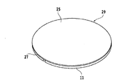
次に、図2及び図3を参照して、ウエーハ11に粘着テープとしての保護テープ29を貼着する方法について説明する。まず、図2(A)に示すように、ウエーハ11の表面11aに糊塗布装置23を使用して糊を霧状に散布して均一厚さに塗布する。
Next, with reference to FIG.2 and FIG.3, the method of sticking the
次いで、図2(B)に示すように、シート層25をウエーハ11の表面11aに塗布された糊層に接着する。これにより、図3に示すように、ウエーハ11の表面に均一厚さの糊層27を有する粘着テープ(保護テープ)29を貼着することができる。シート層25の厚さは均一であるため、保護テープ29の厚さも全体的に均一となる。
Next, as shown in FIG. 2B, the
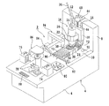
以下、このように構成された半導体ウエーハ11の裏面を所定厚さに研削する研削装置2を図4を参照して説明する。研削装置2のハウジング4は、水平ハウジング部分6と、垂直ハウジング部分8から構成される。
Hereinafter, a grinding
垂直ハウジング部分8には上下方向に伸びる1対のガイドレール12,14が固定されている。この一対のガイドレール12,14に沿って研削手段(研削ユニット)16が上下方向に移動可能に装着されている。研削ユニット16は支持部20を介して一対のガイドレール12,14に沿って上下方向に移動する移動基台18に取り付けられている。
A pair of
研削ユニット16は、支持部20に取り付けられたスピンドルハウジング22と、スピンドルハウジング22中に回転可能に収容されたスピンドル24と、スピンドル24を回転駆動するサーボモータ26を含んでいる。
The grinding
図7に最も良く示されるように、スピンドル24の先端部にはマウンター28が固定されており、このマウンター28には研削ホイール30がねじ止めされている。例えば、研削ホイール30はホイール基台32の自由端部に粒径0.3〜1.0μmのダイヤモンド砥粒をビトリファイドボンドで固めた複数の研削砥石34が固着されて構成されている。よって、研削面は鏡面となる。
As best shown in FIG. 7, a
研削手段(研削ユニット)16にはホース36を介して研削水が供給される。好ましくは、研削水としては純水が使用される。図7に示すように、ホース36から供給された研削水が、スピンドル24に形成された研削水供給穴38、マウンター28に形成された空間40及び研削ホイール30のホイール基台32に形成された複数の研削水供給ノズル42を介して研削砥石34及びチャックテーブル54に保持されたウエーハ11に供給される。
Grinding water is supplied to the grinding means (grinding unit) 16 via a
図4を再び参照すると、研削装置2は、研削ユニット16を一対の案内レール12,14に沿って上下方向に移動する研削ユニット送り機構44を備えている。研削ユニット送り機構44は、ボールねじ46と、ボールねじ46の一端部に固定されたパルスモータ48から構成される。パルスモータ48をパルス駆動すると、ボールねじ46が回転し、移動基台18の内部に固定されたボールねじ46のナットを介して移動基台18が上下方向に移動される。
Referring again to FIG. 4, the grinding
水平ハウジング部分6の凹部10には、チャックテーブルユニット50が配設されている。チャックテーブルユニット50は、図5に示すように、支持基台52と、支持基台52に回転自在に配設されたチャックテーブル54を含んでいる。チャックテーブルユニット50は更に、チャックテーブル54を挿通する穴を有したカバー56を備えている。
A
チャックテーブルユニット50は、チャックテーブル移動機構58により研削装置2の前後方向に移動される。チャックテーブル移動機構58は、ボールねじ60と、ボールねじ60のねじ軸62の一端に連結されたパルスモータ64から構成される。
The
パルスモータ64をパルス駆動すると、ボールねじ60のねじ軸62が回転し、このねじ軸62に螺合したナットを有する支持基台52が研削装置2の前後方向に移動する。よって、チャックテーブル54もパルスモータ64の回転方向に応じて、前後方向に移動する。
When the
図4に示されているように、図5に示した一対のガイドレール66,68及びチャックテーブル移動機構58は蛇腹70,72により覆われている。すなわち、蛇腹70の前端部は凹部10を画成する前壁に固定され、後端部がカバー56の前端面に固定されている。また、蛇腹72の後端は垂直ハウジング部分8に固定され、その前端はカバー56の後端面に固定されている。
As shown in FIG. 4, the pair of
ハウジング4の水平ハウジング部分6には、第1のウエーハカセット74と、第2のウエーハカセット76と、ウエーハ搬送手段78と、ウエーハ仮載置手段80と、ウエーハ搬入手段82と、ウエーハ搬出手段84と、洗浄手段86が配設されている。更に、ハウジング4の前方にはオペレータが研削条件等を入力する操作手段88が設けられている。
In the horizontal housing portion 6 of the housing 4, a
また、水平ハウジング部分6の概略中央部には、チャックテーブル54を洗浄する洗浄水噴射ノズル90が設けられている。この洗浄水噴射ノズル90は、チャックテーブルユニット54がウエーハ搬入・搬出領域に位置づけられた状態において、チャックテーブル54に保持された研削加工後のウエーハに向けて洗浄水を噴出する。
Further, a cleaning
チャックテーブルユニット50は、チャックテーブル移動機構58のパルスモータ64をパルス駆動することにより、図4に示した装置奥側の研削領域と、ウエーハ搬入手段82からウエーハを受け取りウエーハ搬出手段84にウエーハを受け渡す手前側のウエーハ搬入・搬出領域との間で移動される。
The
ウエーハ搬入・搬出領域の上方にはCCDカメラ等を有する撮像装置94が配設されている。この撮像装置94は、ウエーハ11の研削面を撮像し、画像情報を取得する。
An
このように構成された研削装置2の研削作業について以下に説明する。第1のウエーハカセット74中に収容されるウエーハは、保護テープが表面側(回路が形成されている側の面)に装着された半導体ウエーハであり、従ってウエーハは裏面が上側に位置する状態で第1のカセット74中に収容されている。このように複数の半導体ウエーハを収容した第1のウエーハカセット74は、ハウジング4の所定のカセットを搬入領域に載置される。
The grinding operation of the grinding
そして、カセット搬入領域に載置された第1のウエーハカセット74に収容されていた研削加工前の半導体ウエーハが全て搬出されると、空のウエーハカセット74に変えて複数個の半導体ウエーハを収容した新しい第1のウエーハカセット74が手動でカセット搬入領域に載置される。
When all of the unprocessed semiconductor wafers contained in the
一方、ハウジング4の所定のカセット搬出領域に載置された第2のウエーハカセット76に所定枚数の研削加工後の半導体ウエーハが搬入されると、かかる第2のウエーハカセット76は手動で搬出されて、新しい空の第2のウエーハカセット76がカセット搬出領域に載置される。
On the other hand, when a predetermined number of ground semiconductor wafers are loaded into the
第1のウエーハカセット74に収容された半導体ウエーハは、ウエーハ搬送手段78の上下動作及び進退動作により搬送され、ウエーハ仮載置手段80に載置される。ウエーハ仮載置手段80に載置されたウエーハは、ここで中心合わせが行われた後にウエーハ搬入手段82の旋回動作によって、ウエーハ搬入・搬出領域に位置せしめられているチャックテーブルユニット50のチャックテーブル54に載置され、チャックテーブル54によって吸引保持される。
The semiconductor wafer accommodated in the
このようにチャックテーブル54がウエーハを吸引保持したならば、チャックテーブル移動機構58を作動して、チャックテーブルユニット54を移動して装置後方の研削領域に位置づける。
When the chuck table 54 sucks and holds the wafer in this way, the chuck
チャックテーブルユニット50が研削領域に位置づけられると、チャックテーブル54に保持されたウエーハの中心が研削ホイール30の外周円を僅かに超えた位置に位置づけられる。
When the
次に、チャックテーブル54を例えば100〜300rpm程度で回転し、サーボモータ26を駆動して研削ホイール30を4000〜7000rpmで回転するとともに、研削ユニット送り機構44のパルスモータ48を正転駆動して研削ユニット16を下降させる。
Next, the chuck table 54 is rotated at, for example, about 100 to 300 rpm, the
そして、図7に示すように、研削ホイール30の研削砥石34をチャックテーブル54上のウエーハ11の裏面(被研削面)に所定の荷重で押圧することにより、ウエーハ11の裏面が研削される。このようにして所定時間研削することにより、ウエーハ11が所定の厚さに研削される。
As shown in FIG. 7, the back surface of the
研削が終了すると、チャックテーブル移動機構58を駆動してチャックテーブル54を装置手前側のウエーハ搬入・搬出領域に位置付ける。チャックテーブル54がウエーハ搬入・搬出領域に位置付けられたならば、洗浄水噴射ノズル90から洗浄水を噴射して、チャックテーブル54に保持されている研削加工されたウエーハ11の被研削面(裏面)を洗浄する。
When grinding is completed, the chuck
本実施形態によると、粘着テープ(保護テープ)29を構成するシート層25と糊層27とを分離しておき、ウエーハ11に粘着テープ29を貼着する際にシート層25と糊層27と一体化するような粘着テープ貼着方法を採用したので、均一の厚さの保護テープ29をウエーハ11の表面に貼着できるため、ウエーハ11の裏面を研削して均一の所定厚さにウエーハ11を仕上げることができる。
According to this embodiment, the
次に、図8乃至図10を参照して、本発明の粘着テープ貼着方法を切削装置のダイシングテープに使用した例について説明する。まず、図8(A)に示すように、シート層91の表面91aに糊塗布装置23を使用して糊を霧状に散布して均一に塗布し、ダイシングテープ92を作成する。
Next, with reference to FIG. 8 thru | or FIG. 10, the example which used the adhesive tape sticking method of this invention for the dicing tape of the cutting device is demonstrated. First, as shown in FIG. 8 (A), a dicing
次いで、図8(B)に示すように、作業テーブル上に環状フレーム94及びウエーハ11をその裏面11bを上にして載置するとともに、表面側に糊が均一に塗布されたシート層91の裏面91bを上にしてダイシングテープ92を環状フレーム94及びウエーハ11に貼着する。
Next, as shown in FIG. 8B, the
この状態で反転すると、図9に示すようにウエーハ11がダイシングテープ92を介して環状フレーム94に配設された状態となる。
When reversed in this state, the
本実施形態では、ウエーハ11のストリート13を所定深さに切削するために、図10に示す切削装置96を使用する。以下、切削装置96の構成について概略的に説明する。
In this embodiment, a cutting
切削装置96の前面側には、オペレータが加工条件等の装置に対する指示を入力するための操作手段98が設けられている。装置上部には、オペレータに対する案内画面や後述する撮像手段によって撮像された画像が表示されるCRT等の表示手段100が設けられている。
On the front side of the cutting
図9に示すように、ウエーハ11は粘着テープであるダイシングテープ92に貼着され、ダイシングテープ92の外周縁部は環状フレーム94に貼着されている。これにより、ウエーハ11はダイシングテープ92を介してフレーム94に支持された状態となり、図10に示したウエーハカセット102中にウエーハが複数枚(例えば25枚)収容される。ウエーハカセット102は上下動可能なカセットエレベータ104上に載置される。
As shown in FIG. 9, the
ウエーハカセット102の後方には、ウエーハカセット102から切削前のウエーハ11を搬出するとともに、切削後のウエーハをウエーハカセット102に搬入する搬出入手段106が配設されている。
Behind the
ウエーハカセット102と搬出入手段106との間には、搬出入対象のウエーハ11が一時的に載置される領域である仮置き領域108が設けられており、仮置き領域108には、ウエーハ11を一定の位置に位置合わせする位置合わせ手段110が配設されている。
Between the
仮置き領域108の近傍には、ウエーハ11と一体となったフレーム94を吸着して搬送する旋回アームを有する搬送手段112が配設されており、仮置き領域108に搬出されたウエーハ11は、搬送手段112により吸着されてチャックテーブル114上に搬送され、このチャックテーブル114に吸引されるとともに、複数のクランプ116によりフレーム94がクランプされることでチャックテーブル114上に保持される。
In the vicinity of the
チャックテーブル114は、回転可能且つX軸方向に往復動可能に構成されており、チャックテーブル114のX軸方向の移動経路の上方には、ウエーハ11の切削すべきストリートを検出するアライメント手段118が配設されている。
The chuck table 114 is configured to be rotatable and reciprocally movable in the X-axis direction. Above the movement path of the chuck table 114 in the X-axis direction, an
アライメント手段118は、ウエーハ11の表面を撮像する撮像手段120を備えており、撮像により取得した画像に基づき、パターンマッチング等の処理によって切削すべきストリートを検出することができる。撮像手段120によって取得された画像は、表示手段100に表示される。
The
アライメント手段118の左側には、チャックテーブル114に保持されたウエーハ11に対して切削加工を施す切削手段(切削ユニット)122が配設されている。切削手段122はアライメント手段118と一体的に構成されており、両者が連動してY軸方向及びZ軸方向に移動する。
On the left side of the alignment means 118, a cutting means (cutting unit) 122 for cutting the
切削手段122は、回転可能なスピンドル124の先端に切削ブレード126が装着されて構成され、Y軸方向及びZ軸方向に移動可能となっている。切削ブレード126は撮像手段120のX軸方向の延長線上に位置している。
The cutting means 122 is configured by attaching a
このように構成された切削装置96により、チャックテーブル114に保持されたウエーハ11のストリートを所定深さに切削する際には、まずアライメント手段118により少なくとも2点でのパターンマッチング等の手法を使用して切削すべきストリートを検出する。次いで、切削手段122をY軸方向に移動させることにより、切削しようとするストリートと切削ブレード126との位置合わせを行う。
When the street of the
切削しようとするストリートと切削ブレード126との位置合わせが行われた状態で、チャックテーブル114をX軸方向に移動させるとともに、切削ブレード126を高速回転させながら切削手段122を所定距離下降させると、位置合わせされたストリートに所定深さの溝が形成される。
In a state where the street to be cut and the
メモリに記憶されたストリートピッチずつ切削手段122をY軸方向にインデックス送りしながら切削を行うことにより、同方向の全てのストリートに所定深さの溝が形成される。更に、チャックテーブル114を90°回転させてから、上記と同様の切削を行うと、最初のストリートと直交する方向の全てのストリートに所定深さの溝が形成される。 By performing cutting while indexing the cutting means 122 in the Y-axis direction by street pitches stored in the memory, grooves having a predetermined depth are formed in all streets in the same direction. Further, when the chuck table 114 is rotated by 90 ° and then the same cutting as described above is performed, grooves having a predetermined depth are formed in all the streets in the direction orthogonal to the first street.
全てのストリートに所定深さの溝が形成されたウエーハ11はチャックテーブル114をX軸方向に移動してから、Y軸方向に移動可能な搬送手段128により把持されて洗浄装置130まで搬送される。洗浄装置130では、洗浄ノズルから水を噴射しながらウエーハ11を低速回転(例えば300rpm)させることによりウエーハを洗浄する。
The
洗浄後、ウエーハ11を高速回転(例えば3000rpm)させながらエアノズルからエアを噴出させてウエーハ11を乾燥させた後、搬送手段112によりウエーハ11を吸着して仮置き領域108に戻し、更に搬出入手段106によりウエーハカセット102の元の収納場所にウエーハ11が戻される。
After the cleaning, the
本実施形態の粘着テープ貼着方法を採用したダイシングテープ92によると、シート層91に糊層が均一に塗布されているため、ダイシングテープ92の厚さが均一となり、従ってウエーハの全てのストリートに均一深さの溝を形成することができる。
According to the dicing
2 研削装置
11 半導体ウエーハ
16 研削手段(研削ユニット)
23 糊塗布装置
25 シート層
24 スピンドル
29 保護テープ
30 研削ホイール
34 研削砥石
54 チャックテーブル
91 シート層
92 ダイシングテープ
94 環状フレーム
114 チャックテーブル
122 切削手段(切削ユニット)
124 スピンドル
126 切削ブレード
2 Grinding
23
Claims (2)
前記粘着テープはシート層と、該シート層に塗布された糊層とから構成され、
ウエーハの被保持面に粘着テープを貼着する際に、該シート層の糊層塗布面に、又はウエーハの被保持面に糊層を均一に塗布してウエーハの被保持面に前記シート層を貼着することを特徴とする粘着テープ貼着方法。 When a wafer is processed by a processing apparatus having a chuck table for holding a wafer and a processing means for processing the wafer held by the chuck table, an adhesive tape is applied to a surface to be held of the wafer held by the chuck table. Adhesive tape sticking method for sticking
The adhesive tape is composed of a sheet layer and an adhesive layer applied to the sheet layer,
When affixing the adhesive tape to the held surface of the wafer, the adhesive layer is uniformly applied to the adhesive layer application surface of the sheet layer or the held surface of the wafer, and the sheet layer is applied to the held surface of the wafer. Adhesive tape sticking method characterized by sticking.
Priority Applications (1)
| Application Number | Priority Date | Filing Date | Title |
|---|---|---|---|
| JP2007309794A JP2009135254A (en) | 2007-11-30 | 2007-11-30 | Method of sticking adhesive tape |
Applications Claiming Priority (1)
| Application Number | Priority Date | Filing Date | Title |
|---|---|---|---|
| JP2007309794A JP2009135254A (en) | 2007-11-30 | 2007-11-30 | Method of sticking adhesive tape |
Publications (1)
| Publication Number | Publication Date |
|---|---|
| JP2009135254A true JP2009135254A (en) | 2009-06-18 |
Family
ID=40866877
Family Applications (1)
| Application Number | Title | Priority Date | Filing Date |
|---|---|---|---|
| JP2007309794A Pending JP2009135254A (en) | 2007-11-30 | 2007-11-30 | Method of sticking adhesive tape |
Country Status (1)
| Country | Link |
|---|---|
| JP (1) | JP2009135254A (en) |
Cited By (6)
| Publication number | Priority date | Publication date | Assignee | Title |
|---|---|---|---|---|
| JP2011124475A (en) * | 2009-12-14 | 2011-06-23 | Lintec Corp | Sheet sticking device and sheet sticking method |
| KR101282557B1 (en) | 2011-05-06 | 2013-07-04 | 주식회사 야스 | Chuck to hold a substrate |
| JP2013138144A (en) * | 2011-12-28 | 2013-07-11 | Lintec Corp | Sheet application apparatus and sheet application method |
| JP2014030066A (en) * | 2013-11-14 | 2014-02-13 | Lintec Corp | Sheet sticking device and sheet sticking method |
| KR20140097017A (en) * | 2013-01-29 | 2014-08-06 | 닛토덴코 가부시키가이샤 | Pressure-sensitive adhesive tape |
| JP2019096768A (en) * | 2017-11-24 | 2019-06-20 | 株式会社ディスコ | Processing method of plate-like object |
Citations (3)
| Publication number | Priority date | Publication date | Assignee | Title |
|---|---|---|---|---|
| JPH06120337A (en) * | 1992-10-08 | 1994-04-28 | Rohm Co Ltd | Dicing method |
| JP2000183140A (en) * | 1998-12-21 | 2000-06-30 | Toyo Chem Co Ltd | Semiconductor wafer-fixing sheet |
| JP2007048958A (en) * | 2005-08-10 | 2007-02-22 | Renesas Technology Corp | Semiconductor device and manufacturing method thereof |
-
2007
- 2007-11-30 JP JP2007309794A patent/JP2009135254A/en active Pending
Patent Citations (3)
| Publication number | Priority date | Publication date | Assignee | Title |
|---|---|---|---|---|
| JPH06120337A (en) * | 1992-10-08 | 1994-04-28 | Rohm Co Ltd | Dicing method |
| JP2000183140A (en) * | 1998-12-21 | 2000-06-30 | Toyo Chem Co Ltd | Semiconductor wafer-fixing sheet |
| JP2007048958A (en) * | 2005-08-10 | 2007-02-22 | Renesas Technology Corp | Semiconductor device and manufacturing method thereof |
Cited By (8)
| Publication number | Priority date | Publication date | Assignee | Title |
|---|---|---|---|---|
| JP2011124475A (en) * | 2009-12-14 | 2011-06-23 | Lintec Corp | Sheet sticking device and sheet sticking method |
| KR101282557B1 (en) | 2011-05-06 | 2013-07-04 | 주식회사 야스 | Chuck to hold a substrate |
| JP2013138144A (en) * | 2011-12-28 | 2013-07-11 | Lintec Corp | Sheet application apparatus and sheet application method |
| KR20140097017A (en) * | 2013-01-29 | 2014-08-06 | 닛토덴코 가부시키가이샤 | Pressure-sensitive adhesive tape |
| JP2014145019A (en) * | 2013-01-29 | 2014-08-14 | Nitto Denko Corp | Pressure-sensitive adhesive tape |
| KR102205230B1 (en) | 2013-01-29 | 2021-01-20 | 닛토덴코 가부시키가이샤 | Pressure-sensitive adhesive tape |
| JP2014030066A (en) * | 2013-11-14 | 2014-02-13 | Lintec Corp | Sheet sticking device and sheet sticking method |
| JP2019096768A (en) * | 2017-11-24 | 2019-06-20 | 株式会社ディスコ | Processing method of plate-like object |
Similar Documents
| Publication | Publication Date | Title |
|---|---|---|
| JP6385131B2 (en) | Wafer processing method | |
| JP2009043931A (en) | Rear-surface grinding method for wafer | |
| JP2009125915A (en) | Grinding wheel mounting mechanism | |
| JP6732382B2 (en) | Processing device and method of processing workpiece | |
| JP2008155292A (en) | Method and apparatus for machining substrate | |
| KR101757932B1 (en) | Wafer transfer mechanism | |
| JP2009135254A (en) | Method of sticking adhesive tape | |
| JP5068611B2 (en) | Method and apparatus for confirming processing water in processing apparatus | |
| JP2015056510A (en) | Processing method of device wafer | |
| JP5184242B2 (en) | Semiconductor wafer processing equipment | |
| JP2010123823A (en) | Cutting device | |
| JP5455609B2 (en) | Grinding apparatus and wafer grinding method using the grinding apparatus | |
| JP2011108746A (en) | Method for processing wafer | |
| JP2009130315A (en) | Cutting method of wafer | |
| JP2010021330A (en) | Method of processing wafer | |
| JP5225733B2 (en) | Grinding equipment | |
| KR101739975B1 (en) | Wafer supporting plate and method for using wafer supporting plate | |
| JP2018192412A (en) | Processing device | |
| JP5037255B2 (en) | Grinding apparatus and observation method of grinding apparatus | |
| JP5875224B2 (en) | Grinding equipment | |
| JP5700988B2 (en) | Wafer grinding method | |
| JP2012151412A (en) | Grinding method of hard substrate | |
| JP2021114493A (en) | Processing device | |
| JP5313022B2 (en) | Workpiece cutting method | |
| JP5618657B2 (en) | Processing method |
Legal Events
| Date | Code | Title | Description |
|---|---|---|---|
| A621 | Written request for application examination |
Free format text: JAPANESE INTERMEDIATE CODE: A621 Effective date: 20101015 |
|
| A977 | Report on retrieval |
Free format text: JAPANESE INTERMEDIATE CODE: A971007 Effective date: 20120712 |
|
| A131 | Notification of reasons for refusal |
Free format text: JAPANESE INTERMEDIATE CODE: A131 Effective date: 20120717 |
|
| A02 | Decision of refusal |
Free format text: JAPANESE INTERMEDIATE CODE: A02 Effective date: 20121113 |