JP5214121B2 - Light emitting device - Google Patents
Light emitting device Download PDFInfo
- Publication number
- JP5214121B2 JP5214121B2 JP2006214700A JP2006214700A JP5214121B2 JP 5214121 B2 JP5214121 B2 JP 5214121B2 JP 2006214700 A JP2006214700 A JP 2006214700A JP 2006214700 A JP2006214700 A JP 2006214700A JP 5214121 B2 JP5214121 B2 JP 5214121B2
- Authority
- JP
- Japan
- Prior art keywords
- light emitting
- emitting element
- emitting device
- substrate body
- wiring pattern
- Prior art date
- Legal status (The legal status is an assumption and is not a legal conclusion. Google has not performed a legal analysis and makes no representation as to the accuracy of the status listed.)
- Active
Links
Images


Classifications
-
- H—ELECTRICITY
- H01—ELECTRIC ELEMENTS
- H01L—SEMICONDUCTOR DEVICES NOT COVERED BY CLASS H10
- H01L33/00—Semiconductor devices with at least one potential-jump barrier or surface barrier specially adapted for light emission; Processes or apparatus specially adapted for the manufacture or treatment thereof or of parts thereof; Details thereof
- H01L33/48—Semiconductor devices with at least one potential-jump barrier or surface barrier specially adapted for light emission; Processes or apparatus specially adapted for the manufacture or treatment thereof or of parts thereof; Details thereof characterised by the semiconductor body packages
- H01L33/62—Arrangements for conducting electric current to or from the semiconductor body, e.g. lead-frames, wire-bonds or solder balls
-
- H—ELECTRICITY
- H01—ELECTRIC ELEMENTS
- H01L—SEMICONDUCTOR DEVICES NOT COVERED BY CLASS H10
- H01L2224/00—Indexing scheme for arrangements for connecting or disconnecting semiconductor or solid-state bodies and methods related thereto as covered by H01L24/00
- H01L2224/01—Means for bonding being attached to, or being formed on, the surface to be connected, e.g. chip-to-package, die-attach, "first-level" interconnects; Manufacturing methods related thereto
- H01L2224/02—Bonding areas; Manufacturing methods related thereto
- H01L2224/04—Structure, shape, material or disposition of the bonding areas prior to the connecting process
- H01L2224/05—Structure, shape, material or disposition of the bonding areas prior to the connecting process of an individual bonding area
- H01L2224/0554—External layer
- H01L2224/0556—Disposition
- H01L2224/0557—Disposition the external layer being disposed on a via connection of the semiconductor or solid-state body
-
- H—ELECTRICITY
- H01—ELECTRIC ELEMENTS
- H01L—SEMICONDUCTOR DEVICES NOT COVERED BY CLASS H10
- H01L2224/00—Indexing scheme for arrangements for connecting or disconnecting semiconductor or solid-state bodies and methods related thereto as covered by H01L24/00
- H01L2224/01—Means for bonding being attached to, or being formed on, the surface to be connected, e.g. chip-to-package, die-attach, "first-level" interconnects; Manufacturing methods related thereto
- H01L2224/02—Bonding areas; Manufacturing methods related thereto
- H01L2224/04—Structure, shape, material or disposition of the bonding areas prior to the connecting process
- H01L2224/05—Structure, shape, material or disposition of the bonding areas prior to the connecting process of an individual bonding area
- H01L2224/0554—External layer
- H01L2224/0556—Disposition
- H01L2224/05571—Disposition the external layer being disposed in a recess of the surface
-
- H—ELECTRICITY
- H01—ELECTRIC ELEMENTS
- H01L—SEMICONDUCTOR DEVICES NOT COVERED BY CLASS H10
- H01L2224/00—Indexing scheme for arrangements for connecting or disconnecting semiconductor or solid-state bodies and methods related thereto as covered by H01L24/00
- H01L2224/01—Means for bonding being attached to, or being formed on, the surface to be connected, e.g. chip-to-package, die-attach, "first-level" interconnects; Manufacturing methods related thereto
- H01L2224/02—Bonding areas; Manufacturing methods related thereto
- H01L2224/04—Structure, shape, material or disposition of the bonding areas prior to the connecting process
- H01L2224/05—Structure, shape, material or disposition of the bonding areas prior to the connecting process of an individual bonding area
- H01L2224/0554—External layer
- H01L2224/05573—Single external layer
-
- H—ELECTRICITY
- H01—ELECTRIC ELEMENTS
- H01L—SEMICONDUCTOR DEVICES NOT COVERED BY CLASS H10
- H01L2224/00—Indexing scheme for arrangements for connecting or disconnecting semiconductor or solid-state bodies and methods related thereto as covered by H01L24/00
- H01L2224/01—Means for bonding being attached to, or being formed on, the surface to be connected, e.g. chip-to-package, die-attach, "first-level" interconnects; Manufacturing methods related thereto
- H01L2224/10—Bump connectors; Manufacturing methods related thereto
- H01L2224/15—Structure, shape, material or disposition of the bump connectors after the connecting process
- H01L2224/16—Structure, shape, material or disposition of the bump connectors after the connecting process of an individual bump connector
- H01L2224/161—Disposition
- H01L2224/16151—Disposition the bump connector connecting between a semiconductor or solid-state body and an item not being a semiconductor or solid-state body, e.g. chip-to-substrate, chip-to-passive
- H01L2224/16221—Disposition the bump connector connecting between a semiconductor or solid-state body and an item not being a semiconductor or solid-state body, e.g. chip-to-substrate, chip-to-passive the body and the item being stacked
- H01L2224/16225—Disposition the bump connector connecting between a semiconductor or solid-state body and an item not being a semiconductor or solid-state body, e.g. chip-to-substrate, chip-to-passive the body and the item being stacked the item being non-metallic, e.g. insulating substrate with or without metallisation
-
- H—ELECTRICITY
- H01—ELECTRIC ELEMENTS
- H01L—SEMICONDUCTOR DEVICES NOT COVERED BY CLASS H10
- H01L2224/00—Indexing scheme for arrangements for connecting or disconnecting semiconductor or solid-state bodies and methods related thereto as covered by H01L24/00
- H01L2224/01—Means for bonding being attached to, or being formed on, the surface to be connected, e.g. chip-to-package, die-attach, "first-level" interconnects; Manufacturing methods related thereto
- H01L2224/42—Wire connectors; Manufacturing methods related thereto
- H01L2224/47—Structure, shape, material or disposition of the wire connectors after the connecting process
- H01L2224/48—Structure, shape, material or disposition of the wire connectors after the connecting process of an individual wire connector
- H01L2224/4805—Shape
- H01L2224/4809—Loop shape
- H01L2224/48091—Arched
-
- H—ELECTRICITY
- H01—ELECTRIC ELEMENTS
- H01L—SEMICONDUCTOR DEVICES NOT COVERED BY CLASS H10
- H01L2224/00—Indexing scheme for arrangements for connecting or disconnecting semiconductor or solid-state bodies and methods related thereto as covered by H01L24/00
- H01L2224/73—Means for bonding being of different types provided for in two or more of groups H01L2224/10, H01L2224/18, H01L2224/26, H01L2224/34, H01L2224/42, H01L2224/50, H01L2224/63, H01L2224/71
- H01L2224/732—Location after the connecting process
- H01L2224/73251—Location after the connecting process on different surfaces
- H01L2224/73265—Layer and wire connectors
-
- H—ELECTRICITY
- H01—ELECTRIC ELEMENTS
- H01L—SEMICONDUCTOR DEVICES NOT COVERED BY CLASS H10
- H01L2924/00—Indexing scheme for arrangements or methods for connecting or disconnecting semiconductor or solid-state bodies as covered by H01L24/00
- H01L2924/0001—Technical content checked by a classifier
- H01L2924/00014—Technical content checked by a classifier the subject-matter covered by the group, the symbol of which is combined with the symbol of this group, being disclosed without further technical details
-
- H—ELECTRICITY
- H01—ELECTRIC ELEMENTS
- H01L—SEMICONDUCTOR DEVICES NOT COVERED BY CLASS H10
- H01L2924/00—Indexing scheme for arrangements or methods for connecting or disconnecting semiconductor or solid-state bodies as covered by H01L24/00
- H01L2924/01—Chemical elements
- H01L2924/01078—Platinum [Pt]
-
- H—ELECTRICITY
- H01—ELECTRIC ELEMENTS
- H01L—SEMICONDUCTOR DEVICES NOT COVERED BY CLASS H10
- H01L2924/00—Indexing scheme for arrangements or methods for connecting or disconnecting semiconductor or solid-state bodies as covered by H01L24/00
- H01L2924/01—Chemical elements
- H01L2924/01079—Gold [Au]
-
- H—ELECTRICITY
- H01—ELECTRIC ELEMENTS
- H01L—SEMICONDUCTOR DEVICES NOT COVERED BY CLASS H10
- H01L33/00—Semiconductor devices with at least one potential-jump barrier or surface barrier specially adapted for light emission; Processes or apparatus specially adapted for the manufacture or treatment thereof or of parts thereof; Details thereof
- H01L33/48—Semiconductor devices with at least one potential-jump barrier or surface barrier specially adapted for light emission; Processes or apparatus specially adapted for the manufacture or treatment thereof or of parts thereof; Details thereof characterised by the semiconductor body packages
- H01L33/483—Containers
Description
本発明は、発光装置に係り、特に配線基板に接続された発光素子の光を効率よく利用することのできる発光装置に関する。 The present invention relates to a light emitting device, and more particularly to a light emitting device capable of efficiently using light from a light emitting element connected to a wiring board.
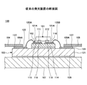
図1は、従来の発光装置の断面図である。 FIG. 1 is a cross-sectional view of a conventional light emitting device.
図1を参照するに、発光装置100は、発光素子101と、サブマウント基板102と、ボード基板103と、外部接続用リード104,105と、放熱板107とを有する。
Referring to FIG. 1, the
発光素子101は、その全面から光を放出する素子である。発光素子101は、給電用端子111,112を有している。発光素子101は、サブマウント基板102に対してフリップチップ接続されている。
The
サブマウント基板102は、はんだ接合よりも熱伝導率の高いAu−Sn接合によりボード基板103上に固定されている。サブマウント基板102は、基板本体114と、配線パターン115,116とを有する。基板本体114は、配線パターン115,116を配設するためのものである。基板本体114の材料としては、熱伝導率の高い材料(例えば、AlN)が用いられる。
The
配線パターン115,116は、基板本体114上に設けられている。配線パターン115は、バンプ118を介して、給電用端子111と電気的に接続されている。配線パターン116は、バンプ118を介して、給電用端子112と電気的に接続されている。サブマウント基板102は、ボード基板103上に配設された部分の外部接続用リード104,105の上面104A,105Aよりも発光素子101を突出させるための基板である。
The
このように、ボード基板103上に配設された部分の外部接続用リード104,105の上面104A,105Aよりも発光素子101を突出させることにより、発光素子101の全面から放出される光を効率よく利用することができる。
In this way, the light emitted from the entire surface of the
ボード基板103は、基板本体121と、配線パターン122,123とを有する。基板本体121は、配線パターン122,123を配設するためのものである。基板本体121の材料としては、熱伝導率の高い材料(例えば、AlNやセラミック等)が用いられる。配線パターン122,123は、基板本体121上に設けられている。配線パターン122は、ワイヤ125Aを介して、配線パターン115と電気的に接続されている。配線パターン123は、ワイヤ125Bを介して、配線パターン116と電気的に接続されている。つまり、サブマウント基板102は、ボード基板103にワイヤボンディング接続されている。
The
外部接続用リード104は、接着剤であるAgペースト127により配線パターン122上に固定されている。外部接続用リード105は、Agペースト127により配線パターン123上に固定されている。
The
放熱板107は、Agペースト129により基板本体121の下面に固定されている。放熱板107は、発光素子101が発光した際に発生する熱を発光装置100の外部に放熱するためのものである。なお、発光素子101が発光した際に発生する熱は、サブマウント基板102及びボード基板103を介して、放熱板107に伝導される(例えば、特許文献1参照。)。
しかしながら、従来の発光装置100では、高価なAu−Snを用いたAu−Sn接合によりサブマウント基板102をボード基板103上に固定していたため、発光装置100のコストが増加するという問題があった。
However, the conventional
そこで本発明は、発光素子の全面から放出される光を効率よく利用することができると共に、コストを低減することのできる発光装置を提供することを目的とする。 In view of the above, an object of the present invention is to provide a light-emitting device that can efficiently use light emitted from the entire surface of a light-emitting element and can reduce costs.
本発明の一観点によれば、発光素子と、基板本体と、前記基板本体に設けられ、前記発光素子と電気的に接続される配線パターンとを有する配線基板と、を備えた発光装置において、前記基板本体は、前記発光素子が配設される部分に、該発光素子を配設する部分が平坦な突出部を有し、前記突出部は、前記突出部の下部から前記突出部の上部に向かうにつれて幅が狭くなるような形状とされており、前記突出部の側面は、傾斜面であり、前記配線パターンは、前記発光素子が配設される側の前記基板本体に設けられており、前記傾斜面には、前記配線パターンが設けられていることを特徴とする発光装置が提供される。 According to one aspect of the present invention, in a light-emitting device including a light-emitting element, a substrate body, and a wiring board provided on the substrate body and having a wiring pattern electrically connected to the light-emitting element, The substrate body has a flat protrusion on a portion where the light emitting element is disposed, and a portion where the light emitting element is disposed, and the protruding portion extends from a lower portion of the protruding portion to an upper portion of the protruding portion. It is shaped so that the width becomes narrower as it goes, the side surface of the protruding portion is an inclined surface, and the wiring pattern is provided on the substrate body on the side where the light emitting element is disposed, A light-emitting device is provided in which the wiring pattern is provided on the inclined surface.
本発明によれば、発光素子が配設される部分に突出部を有した基板本体を用いることにより、従来の発光装置に設けられていたサブマウント基板が不要となる。これにより、発光素子の全面から放出される光を効率よく利用することができると共に、発光装置のコストを低減することができる。また、高価なAu−Sn接合を用いる必要がないため、発光装置のコストを低減することができる。 According to the present invention, the use of the substrate body having the protruding portion at the portion where the light emitting element is disposed eliminates the need for the submount substrate provided in the conventional light emitting device. Thereby, the light emitted from the entire surface of the light emitting element can be used efficiently, and the cost of the light emitting device can be reduced. Further, since it is not necessary to use an expensive Au—Sn junction, the cost of the light-emitting device can be reduced.
本発明の他の観点によれば、第1及び第2の給電用端子を有する発光素子と、前記発光素子が配設される基板本体と、を備えた発光装置において、前記基板本体は、前記発光素子が配設される部分に、該発光素子を配設する部分が平坦な突出部を有し、前記突出部は、前記突出部の下部から前記突出部の上部に向かうにつれて幅が狭くなるような形状とされており、前記突出部の側面は、傾斜面であり、前記突出部が形成された側の前記基板本体に、前記第1の給電用端子と電気的に接続される配線パターンを設け、前記傾斜面には、前記配線パターンが設けられており、前記突出部に前記基板本体を貫通する貫通電極を設け、前記貫通電極と前記第2の給電用端子とを電気的に接続したことを特徴とする発光装置が提供される。
According to another aspect of the present invention, a light emitting device comprising: a light emitting element having first and second power supply terminals; and a substrate body on which the light emitting element is disposed. In the portion where the light emitting element is disposed, the portion where the light emitting element is disposed has a flat protruding portion, and the width of the protruding portion becomes narrower from the lower portion of the protruding portion toward the upper portion of the protruding portion. The side surface of the protrusion is an inclined surface, and the wiring pattern is electrically connected to the first power feeding terminal on the substrate body on the side where the protrusion is formed. The wiring pattern is provided on the inclined surface, a through electrode penetrating the substrate body is provided in the protruding portion, and the through electrode and the second power feeding terminal are electrically connected There is provided a light emitting device characterized by the above.
本発明によれば、発光素子が配設される部分に突出部を有した基板本体を用いると共に、突出部が形成された側の基板本体に第1の給電用端子と電気的に接続される配線パターンを設け、突出部に基板本体を貫通する貫通電極を設け、貫通電極と第2の給電用端子とを電気的に接続することにより、発光素子の全面から放出される光を効率よく利用することができると共に、基板本体のサイズを小型化して、発光装置のコストを低減することができる。 According to the present invention, the substrate main body having the protruding portion at the portion where the light emitting element is disposed is used, and the first power feeding terminal is electrically connected to the substrate main body on the side where the protruding portion is formed. Efficient use of light emitted from the entire surface of the light emitting element by providing a wiring pattern, providing a through electrode penetrating the substrate body in the protruding portion, and electrically connecting the through electrode and the second power supply terminal In addition, the size of the substrate body can be reduced and the cost of the light emitting device can be reduced.
本発明によれば、発光素子の全面から放出される光を効率よく利用することができると共に、発光装置のコストを低減することができる。 According to the present invention, light emitted from the entire surface of the light emitting element can be used efficiently, and the cost of the light emitting device can be reduced.
次に、図面に基づいて本発明の実施の形態について説明する。 Next, embodiments of the present invention will be described with reference to the drawings.
(第1の実施の形態)
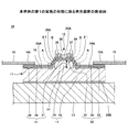
図2は、本発明の第1の実施の形態に係る発光装置の断面図である。
(First embodiment)
FIG. 2 is a cross-sectional view of the light emitting device according to the first embodiment of the present invention.
図2を参照するに、第1の実施の形態の発光装置10は、配線基板11と、発光素子12と、放熱板13と、外部接続用リード14,15とを有する。配線基板11は、基板本体17と、絶縁膜18と、第1の配線パターン21と、第2の配線パターン22とを有する。
Referring to FIG. 2, the
基板本体17は、板部24と、突出部25とを有する。突出部25は、板部24と一体的に構成されている。突出部25は、板部24の上面24A側に設けられており、板部24の上面24Aから突出している。突出部25の上面25Aは、第1の配線パターン21上に設けられた部分の外部接続用リード14の上面14A、及び第2の配線パターン22上に設けられた部分の外部接続用リード15の上面15Aよりも突出するように形成されている。
The
突出部25は、第1の配線パターン21に設けられた部分の外部接続用リード14の上面14A、及び第2の配線パターン22に設けられた部分の外部接続用リード15の上面15Aよりも発光素子12の位置が高くなるように設定するためのものである。突出部25の高さH1(板部24の上面24Aを基準としたときの高さ)は、例えば、400μmとすることができる。
The
このように、第1の配線パターン21に設けられた部分の外部接続用リード14の上面14A、及び第2の配線パターン22に設けられた部分の外部接続用リード15の上面15Aよりも発光素子12の位置を高くするための突出部25を基板本体17に設けることにより、従来の発光装置100に設けられていたサブマウント基板102が不要となるため、発光素子12の全面から放出される光を効率よく利用することができる。また、発光装置10の場合、従来の発光装置100のように2つの基板(サブマウント基板102及びボード基板103)を設ける必要がなく、1つの配線基板11を設ければよいため、発光装置10のコストを低減することができる。
In this way, the light emitting element is more than the
突出部25は、突出部25の下部から突出部25の上部(突出部25の上面25A)に向かうにつれて幅が狭くなるような形状とされている。突出部25の側面25Bは、板部24の上面24Aと所定角度θ1を成す傾斜面とされている。所定角度θ1は、例えば、54.7度や90度とすることができる。
The protruding
このように、突出部25の側面25Bを傾斜面とすることにより、段差部A,Bに形成された部分の第1及び第2の配線パターン21,22への応力集中が緩和されるため、第1及び第2の配線パターン21,22の破損(例えば、断線)を防止することができる。
As described above, since the side surface 25B of the protruding
基板本体17の材料としては、シリコンを用いることができる。基板本体17の材料としてシリコンを用いることにより、傾斜面とされた側面25Bを有した突出部25を容易に形成することができる。
Silicon can be used as the material of the
絶縁膜18は、板部24の上面24A及び突出部25の上面25A及び側面25Bに設けられている。絶縁膜18は、基板本体17と第1及び第2の配線パターン21,22との間を絶縁するための膜である。
The insulating
第1の配線パターン21は、発光素子接続用パッド27と、リード接続部28と、配線部29とを有する。発光素子接続用パッド27は、突出部25の上面25Aに形成された絶縁膜18上に設けられている。発光素子接続用パッド27は、発光素子12の第1の給電用端子36と電気的に接続されている。
The
リード接続部28は、板部24の上面24Aに形成された絶縁膜18上に設けられている。リード接続部28は、外部接続用リード14と電気的に接続されている。
The
配線部29は、突出部25の側面25B及び板部24の上面24Aに形成された絶縁膜18上に設けられている。配線部29は、一方の端部が発光素子接続用パッド27と接続されており、他方の端部がリード接続部28と接続されている。配線部29は、発光素子接続用パッド27とリード接続部28とを電気的に接続するためのものである。
The
第2の配線パターン22は、発光素子接続用パッド32と、リード接続部33と、配線部34とを有する。発光素子接続用パッド32は、突出部25の上面25Aに形成された絶縁膜18上に設けられている。発光素子接続用パッド32は、発光素子12の第2の給電用端子37と電気的に接続されている。
The
リード接続部33は、板部24の上面24Aに形成された絶縁膜18上に設けられている。リード接続部33は、外部接続用リード15と電気的に接続されている。
The
配線部34は、突出部25の側面25B及び板部24の上面24Aに形成された絶縁膜18上に設けられている。配線部34は、一方の端部が発光素子接続用パッド32と接続されており、他方の端部がリード接続部33と接続されている。配線部34は、発光素子接続用パッド32とリード接続部33とを電気的に接続するためのものである。
The
発光素子12は、その全面から光を放出する素子である。発光素子12は、第1の給電用端子36と、第2の給電用端子37とを有する。第1の給電用端子36は、バンプ38を介して、発光素子接続用パッド27と電気的に接続されている。第2の給電用端子37は、バンプ39を介して、発光素子接続用パッド32と電気的に接続されている。つまり、発光素子12は、第1及び第2の配線パターン21,22に対してフリップチップ接続されている。
The
発光素子12は、第1の配線パターン21と接続された部分の外部接続用リード14の上面14A、及び第2の配線パターン22と接続された部分の外部接続用リード15の上面15Aよりも高い位置に配設されている。
The
このように、第1の配線パターン21と接続された部分の外部接続用リード14の上面14A、及び第2の配線パターン22と接続された部分の外部接続用リード15の上面15Aよりも高い位置に発光素子12を配設することにより、発光素子12の全面から放出された光を効率よく利用することができる。
As described above, the position is higher than the
放熱板13は、接着剤であるAgペーストにより板部24の下面24Bに接着されている。このように、板部24の下面24Bに放熱板13を設けることにより、発光素子12が発光した際に発生する熱を放熱することができる。
The
外部接続用リード14は、接着剤であるAgペーストによりリード接続部28上に接着されている。外部接続用リード14は、第1の配線パターン21を介して、第1の給電用端子36と電気的に接続されている。
The
外部接続用リード15は、接着剤であるAgペーストによりリード接続部33上に接着されている。外部接続用リード15は、第2の配線パターン22を介して、第2の給電用端子37と電気的に接続されている。外部接続用リード14,15は、図示していない電源と接続されている。
The
本実施の形態の発光装置によれば、配線基板11と接続された部分の外部接続用リード14,15の上面14A,15Aの位置よりも発光素子12を突出させる突出部25を基板本体17に設けることにより、従来の発光装置100に設けられていたサブマウント基板102が不要となるので、発光素子12の光を効率よく利用することができる。また、発光装置10の場合、従来の発光装置100のように2つの基板(サブマウント基板102及びボード基板103)を設ける必要がなく、1つの配線基板11を設ければよいため、発光装置10のコストを低減することができる。
According to the light emitting device of the present embodiment, the protruding
また、高価なAu−Sn接合を用いる必要がなくなるため、発光装置10のコストを低減することができる。
Moreover, since it is not necessary to use an expensive Au—Sn junction, the cost of the
さらに、第1の配線パターン21によりバンプ38と外部接続用リード14とを電気的に接続すると共に、第2の配線パターン22によりバンプ39と外部接続用リード15とを電気的に接続することにより、従来の発光装置100に設けられていたワイヤ125A,125B(図1参照)が不要となるため、発光素子12と外部接続用リード14,15との間の電気的接続信頼性を向上させることができる。
Further, the
なお、本実施の形態の発光装置10では、接着剤としてAgペーストを用いた場合を例に挙げて説明したが、導電性の接着剤であればAgペースト以外の接着剤でもよい。
In the
また、本実施の形態の発光装置10では、外部接続用リード14と第1の配線パターン21との接続、及び外部接続用リード15と第2の配線パターン22との接続にAgペーストを用いた場合を例に挙げたが、Agペースト等の導電性の接着剤を用いることなく、外部接続用リード14と第1の配線パターン21とを電気的に接続すると共に、外部接続用リード15と第2の配線パターン22とを電気的に接続してもよい。具体的には、例えば、配線基板11及び放熱板13を収容ケースに収容し、外部接続用リード14,15に発光素子12を露出する枠体を押し当て、枠体を収容ケースに係止させてもよい。
In the
(第2の実施の形態)
図3は、本発明の第2の実施の形態に係る発光装置の断面図である。
(Second Embodiment)
FIG. 3 is a cross-sectional view of a light emitting device according to the second embodiment of the present invention.
図3を参照するに、第2の実施の形態の発光装置50は、外部接続用リード14,15と、配線基板51と、放熱板52と、発光素子12とを有する。
Referring to FIG. 3, the
配線基板51は、基板本体54と、絶縁膜18と、第1の配線パターン21と、貫通電極55とを有する。基板本体54は、板部61と、突出部62とを有する。突出部62は、板部61と一体的に構成されている。突出部62は、板部61の上面61A側に設けられており、板部61の上面61Aから突出している。突出部62の上面62Aは、第1の配線パターン21に設けられた部分の外部接続用リード14の上面14Aよりも突出するように形成されている。
The
突出部62は、第1の配線パターン21に設けられた部分の外部接続用リード14の上面14Aよりも発光素子12を突出させるためのものである。突出部62の高さH2(板部61の上面61Aを基準としたときの高さ)は、例えば、400μmとすることができる。
The projecting
このように、配線基板51に接続された部分の外部接続用リード14の上面14Aよりも発光素子12を突出させる突出部62を基板本体54に設けることにより、従来の発光装置100に設けられたサブマウント基板102(図1参照)が不要となるため、発光素子12の全面から放出される光を効率よく利用することができる。また、発光装置50の場合、従来の発光装置100のように2つの基板(サブマウント基板102及びボード基板103)を設ける必要がなく、1つの配線基板51を設ければよいため、発光装置50のコストを低減することができる。
As described above, the
突出部62は、絶縁膜18が形成される側面62Bを有する。突出部62の側面62Bは、板部61の上面61Aと所定角度θ2を成す傾斜面とされている。所定角度θ2は、例えば、54.7度や90度とすることができる。
The
このように、突出部62の側面62Bを傾斜面とすることにより、段差部C,Dに形成された部分の第1の配線パターン21に応力が集中することがなくなるため、第1の配線パターン21の破損(例えば、断線)を防止することができる。
As described above, since the side surface 62B of the projecting
基板本体54には、突出部62及び突出部62の下方に位置する板部61を貫通する貫通孔65が形成されている。
The
基板本体54の材料としては、シリコンを用いることができる。基板本体54の材料としてシリコンを用いることにより、傾斜面とされた側面62Bを有した突出部62を容易に形成することができる。
As a material of the
絶縁膜18は、板部61の上面61A及び突出部62の上面62A及び側面62Bを覆うように設けられている。絶縁膜18は、第1の配線パターン21と貫通電極55との間を絶縁するための膜である。
The insulating
第1の配線パターン21は、発光素子接続用パッド27と、リード接続部28と、配線部29とを有する。発光素子接続用パッド27は、突出部62に形成された絶縁膜18上に設けられている。発光素子接続用パッド27は、バンプ56を介して、発光素子12の第1の給電用端子36と電気的に接続されている。
The
リード接続部28は、板部61の上面61Aに形成された絶縁膜18上に設けられている。リード接続部28は、外部接続用リード14と電気的に接続されている。
The
配線部29は、突出部62の側面62B及び板部61の上面61Aに形成された絶縁膜18上に設けられている。配線部29は、一方の端部が発光素子接続用パッド27と接続されており、他方の端部がリード接続部28と接続されている。配線部29は、発光素子接続用パッド27とリード接続部28とを電気的に接続するためのものである。
The
貫通電極55は、貫通孔65に設けられている。貫通電極55の上端部は、絶縁膜18の上面18Aと略面一とされている。貫通電極55の上端部は、バンプ57を介して、発光素子12の第2の給電用端子37と電気的に接続されている。貫通電極55の下端部は、板部61の下面61Bと略面一とされている。貫通電極55の下端部は、接着剤であるAgペーストを介して、導電性を有した放熱板52と電気的及び熱的に接続されている。
The through
貫通電極55の材料としては、例えば、シリコンよりも熱伝導率が高く、かつ導電性を有した材料を用いるとよい。具体的には、貫通電極55の材料としては、Cuを用いることができる。また、貫通電極55は、例えば、めっき法により形成することができる。
As a material of the through
このように、突出部62及び突出部62の下方に位置する板部61を貫通する貫通電極55を設け、貫通電極55と第2の給電用端子37とを電気的に接続することにより、基板本体54のサイズを小型化することが可能となる。これにより、発光装置50のコストを低減することができる。
Thus, by providing the through-
また、シリコンよりも熱伝導率が高く、かつ導電性を有した材料により貫通電極55を構成することにより、発光素子12が発光した際の熱を放熱板52に効率よく伝達することができる。
In addition, by forming the through
放熱板52は、接着剤であるAgペーストにより配線基板51の下面51Bに接着されている。放熱板52の材料としては、導電性を有し、熱伝導率の高い材料が好ましい。具体的には、放熱板52の材料としては、例えば、熱伝導率の高いCuを用いることができる。
The
このように、導電性を有した材料により放熱板52を構成することにより、貫通電極55と外部接続用リード15との間を電気的に接続することができる。
Thus, by forming the
また、導電性を有し、熱伝導率の高い材料により放熱板52を構成することにより、放熱板52の放熱特性を向上させることができる。
Moreover, the heat dissipation characteristic of the
外部接続用リード14は、接着剤であるAgペーストによりリード接続部28上に接着されている。これにより、外部接続用リード14は、第1の配線パターン21を介して、第1の給電用電極36と電気的に接続される。
The
外部接続用リード15は、接着剤であるAgペーストにより放熱板52上に接着されている。これにより、外部接続用リード15は、放熱板52及び貫通電極55を介して、第2の給電用電極37と電気的に接続される。
The
発光素子12は、第1の配線パターン21に設けられた部分の外部接続用リード14の上面14Aよりも高い位置に配設されている。このように、第1の配線パターン21上に設けられた部分の外部接続用リード14の上面14Aよりも高い位置に発光素子12を配設することにより、発光素子12の全面から放出される光を効率よく利用することができる。
The
発光素子12は、第1の給電用端子36と、第2の給電用端子37とを有する。第1の給電用端子36は、バンプ56を介して、発光素子接続用パッド27と電気的に接続されている。第2の給電用端子37は、バンプ57を介して、貫通電極55と電気的に接続されている。
The
本実施の形態の発光装置によれば、突出部62及び突出部62の下方に位置する板部61を貫通する貫通電極55を設け、貫通電極55と第2の給電用端子37とを電気的に接続することにより、基板本体54のサイズを小型化することが可能となるため、発光装置50のコストを低減することができる。
According to the light emitting device of the present embodiment, the projecting
また、シリコンよりも熱伝導率が高く、かつ導電性を有した材料により貫通電極55を構成することにより、発光素子12が発光した際の熱を放熱板52に効率よく伝達することができる。
In addition, by forming the through
さらに、本実施の形態の発光装置50は、第1の実施の形態の発光装置10と同様な効果を得ることができる。
Furthermore, the
なお、本実施の形態の発光装置50では、接着剤としてAgペーストを用いた場合を例に挙げて説明したが、導電性の接着剤であればAgペースト以外の接着剤でもよい。
In the
また、本実施の形態の発光装置50では、外部接続用リード14と第1の配線パターン21との接続、及び外部接続用リード15と放熱板52との接続にAgペーストを用いた場合を例に挙げて説明したが、Agペースト等の導電性の接着剤を用いることなく、外部接続用リード14と第1の配線パターン21とを電気的に接続すると共に、外部接続用リード15と放熱板52とを電気的に接続してもよい。具体的には、例えば、配線基板51及び放熱板52を収容ケースに収容し、外部接続用リード14,15に発光素子12を露出する枠体を押し当て、枠体を収容ケースに係止させてもよい。
Further, in the
(第3の実施の形態)
図4は、本発明の第3の実施の形態に係る発光装置の断面図である。
(Third embodiment)
FIG. 4 is a cross-sectional view of a light emitting device according to the third embodiment of the present invention.
図4を参照するに、第3の実施の形態の発光装置70は、第2の実施の形態の発光装置50に設けられた配線基板51の代わりに配線基板71を設けた以外は発光装置50と同様に構成される。
Referring to FIG. 4, a
配線基板71は、第2の実施の形態で説明した配線基板51の構成にさらに金属層72を設けた以外は配線基板51と同様な構成とされている。
The
金属層72は、熱伝導率の高い金属から構成されている。金属層72は、板部61の下面61Bに形成されている。金属層72は、貫通電極55の下端部と接続されている。これにより、金属層72は、貫通電極55を介して、第2の給電用端子37と電気的及び熱的に接続されている。
The
金属層72は、接着剤であるAgペーストにより放熱板52上に固定されている。つまり、金属層72は、板部61と放熱板52との間に配置されている。これにより、放熱板52は、発光素子12の第2の給電用端子37と電気的及び熱的に接続される。金属層72の材料としては、例えば、Cuを用いることができる。金属層72は、例えば、めっき法やスパッタ法により形成することができる。金属層72の厚さは、例えば、5μmとすることができる。
The
本実施の形態の発光装置によれば、貫通電極55と接続された熱伝導率の高い金属層72を板部61と放熱板52との間に設けることにより、発光素子12が発光した際に発生する熱を効率よく放熱板52に伝達することが可能となるので、放熱効率を向上させることができる。
According to the light emitting device of the present embodiment, when the
なお、本実施の形態の発光装置70では、接着剤であるAgペーストを用いて放熱板52上に金属層72を固定した場合を例に挙げて説明したが、Agペーストを用いることなく、直接接合法を用いて放熱板52上に金属層72を固定してもよい。直接接合法としては、例えば、金属層72の下面72A及び放熱板52の上面52Aをそれぞれプラズマにより活性化して平滑な面とし、その後、金属層72の下面72Aを放熱板52の上面52Aに押し当てて、金属層72と放熱板52とを接合させる方法を用いることができる。このとき、金属層72及び放熱板52を加熱して接合させてもよい。
In the
このような直接接合法を用いて、金属層72を放熱板52上に固定することにより、熱伝導率のあまりよくないAgペーストが不要となり、金属層72と放熱板52とが直接接触するため、発光素子12が発光した際に発生する熱をさらに効率よく放熱することができる。
By fixing the
また、本実施の形態の発光装置70では、接着剤としてAgペーストを用いた場合を例に挙げて説明したが、導電性の接着剤であればAgペースト以外の接着剤でもよい。
Further, in the
さらに、本実施の形態の発光装置70では、外部接続用リード14と第1の配線パターン21との接続、及び外部接続用リード15と放熱板52との接続にAgペーストを用いたが、Agペースト等の導電性の接着剤を用いることなく、外部接続用リード14と第1の配線パターン21とを電気的に接続すると共に、外部接続用リード15と放熱板52とを電気的に接続してもよい。具体的には、例えば、配線基板71及び放熱板52を収容ケースに収容し、外部接続用リード14,15に発光素子12を露出する枠体を押し当て、枠体を収容ケースに係止させてもよい。
Further, in the
以上、本発明の好ましい実施の形態について詳述したが、本発明はかかる特定の実施の形態に限定されるものではなく、特許請求の範囲内に記載された本発明の要旨の範囲内において、種々の変形・変更が可能である。 The preferred embodiments of the present invention have been described in detail above, but the present invention is not limited to such specific embodiments, and within the scope of the present invention described in the claims, Various modifications and changes are possible.
本発明によれば、発光素子の全面から放出された光を効率よく利用することができると共に、コストを低減することのできる発光装置に適用可能である。 The present invention can be applied to a light-emitting device that can efficiently use light emitted from the entire surface of the light-emitting element and reduce cost.
10,50,70 発光装置
11,51,71 配線基板
12 発光素子
13,52 放熱板
14,15 外部接続用リード
14A,15A,18A,24A,25A,52A,61A 上面
17,54 基板本体
18 絶縁膜
21 第1の配線パターン
22 第2の配線パターン
24,61 板部
24B,61B,72A 下面
25,62 突出部
25B,62B 側面
27,32 発光素子接続用パッド
28,33 リード接続部
29,34 配線部
36 第1の給電用端子
37 第2の給電用端子
38,39,56,57 バンプ
55 貫通電極
65 貫通孔
72 金属層
A,B,C,D 段差部
H1,H2 高さ
θ1,θ2 角度
10, 50, 70 Light-emitting
Claims (9)
基板本体と、前記基板本体に設けられ、前記発光素子と電気的に接続される配線パターンとを有する配線基板と、を備えた発光装置において、
前記基板本体は、前記発光素子が配設される部分に、該発光素子を配設する部分が平坦な突出部を有し、
前記突出部は、前記突出部の下部から前記突出部の上部に向かうにつれて幅が狭くなるような形状とされており、
前記突出部の側面は、傾斜面であり、
前記配線パターンは、前記発光素子が配設される側の前記基板本体に設けられており、
前記傾斜面には、前記配線パターンが設けられていることを特徴とする発光装置。 A light emitting element;
In a light emitting device comprising: a substrate body; and a wiring substrate provided on the substrate body and having a wiring pattern electrically connected to the light emitting element.
The substrate body has a flat protrusion at a portion where the light emitting element is disposed, and a portion where the light emitting element is disposed,
The protrusion is shaped so that the width decreases from the lower part of the protrusion toward the upper part of the protrusion,
The side surface of the protrusion is an inclined surface,
The wiring pattern is provided on the substrate body on the side where the light emitting element is disposed,
The light emitting device, wherein the inclined surface is provided with the wiring pattern.
前記突出部は、前記基板本体に設けられた部分の前記外部接続用リードの上面よりも突出することを特徴とする請求項1記載の発光装置。 An external connection lead electrically connected to the wiring pattern;
The light emitting device according to claim 1, wherein the protruding portion protrudes from an upper surface of the external connection lead of a portion provided on the substrate body.
前記発光素子が配設される基板本体と、を備えた発光装置において、
前記基板本体は、前記発光素子が配設される部分に、該発光素子を配設する部分が平坦な突出部を有し、
前記突出部は、前記突出部の下部から前記突出部の上部に向かうにつれて幅が狭くなるような形状とされており、
前記突出部の側面は、傾斜面であり、
前記突出部が形成された側の前記基板本体に、前記第1の給電用端子と電気的に接続される配線パターンを設け、
前記傾斜面には、前記配線パターンが設けられており、
前記突出部に前記基板本体を貫通する貫通電極を設け、前記貫通電極と前記第2の給電用端子とを電気的に接続したことを特徴とする発光装置。 A light emitting device having first and second power supply terminals;
In a light emitting device comprising a substrate body on which the light emitting element is disposed,
The substrate body has a flat protrusion at a portion where the light emitting element is disposed, and a portion where the light emitting element is disposed,
The protrusion is shaped so that the width decreases from the lower part of the protrusion toward the upper part of the protrusion,
The side surface of the protrusion is an inclined surface,
A wiring pattern electrically connected to the first power feeding terminal is provided on the substrate body on the side where the protruding portion is formed,
The inclined surface is provided with the wiring pattern,
A light emitting device, wherein a through electrode penetrating the substrate body is provided in the protruding portion, and the through electrode and the second power feeding terminal are electrically connected.
前記配線パターンは、前記発光素子が配設される側の前記基板本体に設けられており、
前記突出部は、前記基板本体に設けられた部分の前記外部接続用リードの上面よりも突出することを特徴とする請求項5記載の発光装置。 An external connection lead electrically connected to the wiring pattern;
The wiring pattern is provided on the substrate body on the side where the light emitting element is disposed,
6. The light emitting device according to claim 5, wherein the protruding portion protrudes from an upper surface of the external connection lead at a portion provided on the substrate body.
Priority Applications (4)
| Application Number | Priority Date | Filing Date | Title |
|---|---|---|---|
| JP2006214700A JP5214121B2 (en) | 2006-08-07 | 2006-08-07 | Light emitting device |
| US11/882,812 US7816690B2 (en) | 2006-08-07 | 2007-08-06 | Light-emitting device |
| TW096128945A TW200810160A (en) | 2006-08-07 | 2007-08-07 | Light-emitting device |
| EP07015539.5A EP1887635B1 (en) | 2006-08-07 | 2007-08-07 | Light-emitting device |
Applications Claiming Priority (1)
| Application Number | Priority Date | Filing Date | Title |
|---|---|---|---|
| JP2006214700A JP5214121B2 (en) | 2006-08-07 | 2006-08-07 | Light emitting device |
Publications (3)
| Publication Number | Publication Date |
|---|---|
| JP2008041953A JP2008041953A (en) | 2008-02-21 |
| JP2008041953A5 JP2008041953A5 (en) | 2009-08-13 |
| JP5214121B2 true JP5214121B2 (en) | 2013-06-19 |
Family
ID=38657872
Family Applications (1)
| Application Number | Title | Priority Date | Filing Date |
|---|---|---|---|
| JP2006214700A Active JP5214121B2 (en) | 2006-08-07 | 2006-08-07 | Light emitting device |
Country Status (4)
| Country | Link |
|---|---|
| US (1) | US7816690B2 (en) |
| EP (1) | EP1887635B1 (en) |
| JP (1) | JP5214121B2 (en) |
| TW (1) | TW200810160A (en) |
Families Citing this family (6)
| Publication number | Priority date | Publication date | Assignee | Title |
|---|---|---|---|---|
| TWI353657B (en) * | 2007-09-28 | 2011-12-01 | Ind Tech Res Inst | An island submount |
| CN102881812B (en) * | 2011-07-15 | 2015-03-25 | 赛恩倍吉科技顾问(深圳)有限公司 | Manufacturing method for Light emitting diode packaging structure |
| JP6006525B2 (en) * | 2012-05-15 | 2016-10-12 | スタンレー電気株式会社 | Semiconductor light emitting device and lamp using the same |
| KR101978941B1 (en) * | 2013-01-28 | 2019-05-15 | 엘지이노텍 주식회사 | Light Emitting Device Package |
| KR102153041B1 (en) * | 2013-12-04 | 2020-09-07 | 삼성전자주식회사 | Semiconductor device package and method of manufacturing the same |
| US20220246594A1 (en) * | 2019-06-11 | 2022-08-04 | Kyocera Corporation | Light emitter board and display device |
Family Cites Families (20)
| Publication number | Priority date | Publication date | Assignee | Title |
|---|---|---|---|---|
| JPS54389B2 (en) * | 1975-05-06 | 1979-01-10 | ||
| JPH0513820A (en) * | 1991-07-02 | 1993-01-22 | Omron Corp | Semiconductor device |
| DE4242842C2 (en) * | 1992-02-14 | 1999-11-04 | Sharp Kk | Light-emitting component for surface mounting and method for its production |
| DE10006738C2 (en) * | 2000-02-15 | 2002-01-17 | Osram Opto Semiconductors Gmbh | Light-emitting component with improved light decoupling and method for its production |
| DE10122705B4 (en) * | 2000-05-11 | 2012-07-26 | Mitutoyo Corp. | Device with functional component and method for its production |
| DE10163799B4 (en) * | 2000-12-28 | 2006-11-23 | Matsushita Electric Works, Ltd., Kadoma | Semiconductor chip mounting substrate and method of manufacturing such a mounting substrate |
| DE10105802A1 (en) * | 2001-02-07 | 2002-08-08 | Patent Treuhand Ges Fuer Elektrische Gluehlampen Mbh | Semiconductor component with reflector |
| JP2003031895A (en) * | 2001-07-13 | 2003-01-31 | Sharp Corp | Semiconductor light emitting device and its manufacturing method |
| JP4045781B2 (en) * | 2001-08-28 | 2008-02-13 | 松下電工株式会社 | Light emitting device |
| DE10148227B4 (en) * | 2001-09-28 | 2015-03-05 | Osram Opto Semiconductors Gmbh | Radiation-emitting semiconductor chip, method for its production and radiation-emitting component |
| JP3912607B2 (en) * | 2002-06-19 | 2007-05-09 | サンケン電気株式会社 | Manufacturing method of semiconductor light emitting device |
| JP3993475B2 (en) * | 2002-06-20 | 2007-10-17 | ローム株式会社 | LED chip mounting structure and image reading apparatus having the same |
| US7579629B2 (en) * | 2003-04-01 | 2009-08-25 | Sharp Kabushiki Kaisha | Light-emitting apparatus package, light-emitting apparatus, backlight apparatus, and display apparatus |
| JP4192742B2 (en) * | 2003-09-30 | 2008-12-10 | 豊田合成株式会社 | Light emitting device |
| JP2005136224A (en) * | 2003-10-30 | 2005-05-26 | Asahi Kasei Electronics Co Ltd | Light-emitting diode illumination module |
| TWI227570B (en) * | 2003-12-11 | 2005-02-01 | South Epitaxy Corp | Light-emitting diode packaging structure |
| JP2005203448A (en) | 2004-01-13 | 2005-07-28 | Toyoda Gosei Co Ltd | Light emitter |
| JP4614679B2 (en) | 2004-01-29 | 2011-01-19 | 京セラ株式会社 | LIGHT EMITTING DEVICE, ITS MANUFACTURING METHOD, AND LIGHTING DEVICE |
| JP2006135276A (en) * | 2004-10-04 | 2006-05-25 | Hitachi Ltd | Semiconductor light emitting element mounting package and its manufacturing method |
| JP2006324324A (en) * | 2005-05-17 | 2006-11-30 | Sumitomo Electric Ind Ltd | Light emitting device, method of manufacturing same, and semiconductor substrate |
-
2006
- 2006-08-07 JP JP2006214700A patent/JP5214121B2/en active Active
-
2007
- 2007-08-06 US US11/882,812 patent/US7816690B2/en active Active
- 2007-08-07 EP EP07015539.5A patent/EP1887635B1/en active Active
- 2007-08-07 TW TW096128945A patent/TW200810160A/en unknown
Also Published As
| Publication number | Publication date |
|---|---|
| EP1887635A2 (en) | 2008-02-13 |
| EP1887635B1 (en) | 2017-05-10 |
| JP2008041953A (en) | 2008-02-21 |
| US7816690B2 (en) | 2010-10-19 |
| US20080030139A1 (en) | 2008-02-07 |
| TW200810160A (en) | 2008-02-16 |
| EP1887635A3 (en) | 2012-12-26 |
Similar Documents
| Publication | Publication Date | Title |
|---|---|---|
| US9000474B2 (en) | Wiring substrate, light emitting device, and manufacturing method of wiring substrate | |
| JP4841836B2 (en) | Method for manufacturing light emitting device of flip chip type light emitting diode | |
| TWI645580B (en) | Light emitting diode crystal grain and display using the same | |
| JP5940799B2 (en) | Electronic component mounting package, electronic component package, and manufacturing method thereof | |
| JP5214121B2 (en) | Light emitting device | |
| JP2011108924A (en) | Heat conducting substrate and method for mounting electronic component on the same | |
| JP2009054801A (en) | Heat radiation member, and light emitting module equipped with the same | |
| JP2004228240A (en) | Package for storing light emitting element and light emitting device | |
| JP6043049B2 (en) | Semiconductor device mounting structure and semiconductor device mounting method | |
| JP2003101076A (en) | Light-emitting device | |
| JP2011159951A (en) | Led module device and method of manufacturing the same | |
| JP5697924B2 (en) | Light emitting device | |
| JP2008277626A (en) | Light-emitting device and manufacturing method thereof | |
| JP2006120996A (en) | Circuit module | |
| JP4831958B2 (en) | Surface mount type LED | |
| JP2009088373A (en) | Led lamp module | |
| JP5912471B2 (en) | Semiconductor device | |
| JP2007012718A (en) | Electronic component housing package and electronic device | |
| JP2011086737A (en) | Thermoelectric conversion module | |
| JP2009158769A (en) | Semiconductor device | |
| JP3157844U (en) | Semiconductor element | |
| KR100638881B1 (en) | Led assembly having led package inserted into metal board | |
| KR100575639B1 (en) | Optical signal storage module being united entirely heat sink plate and pcb | |
| JP3130857U (en) | Semiconductor element | |
| JP2006186000A (en) | High power semiconductor device and its manufacturing method |
Legal Events
| Date | Code | Title | Description |
|---|---|---|---|
| A521 | Written amendment |
Free format text: JAPANESE INTERMEDIATE CODE: A523 Effective date: 20090626 |
|
| A621 | Written request for application examination |
Free format text: JAPANESE INTERMEDIATE CODE: A621 Effective date: 20090626 |
|
| A977 | Report on retrieval |
Free format text: JAPANESE INTERMEDIATE CODE: A971007 Effective date: 20110819 |
|
| A131 | Notification of reasons for refusal |
Free format text: JAPANESE INTERMEDIATE CODE: A131 Effective date: 20110823 |
|
| A521 | Written amendment |
Free format text: JAPANESE INTERMEDIATE CODE: A523 Effective date: 20111020 |
|
| A131 | Notification of reasons for refusal |
Free format text: JAPANESE INTERMEDIATE CODE: A131 Effective date: 20120619 |
|
| A521 | Written amendment |
Free format text: JAPANESE INTERMEDIATE CODE: A523 Effective date: 20120808 |
|
| TRDD | Decision of grant or rejection written | ||
| A01 | Written decision to grant a patent or to grant a registration (utility model) |
Free format text: JAPANESE INTERMEDIATE CODE: A01 Effective date: 20130226 |
|
| A61 | First payment of annual fees (during grant procedure) |
Free format text: JAPANESE INTERMEDIATE CODE: A61 Effective date: 20130227 |
|
| R150 | Certificate of patent or registration of utility model |
Ref document number: 5214121 Country of ref document: JP Free format text: JAPANESE INTERMEDIATE CODE: R150 Free format text: JAPANESE INTERMEDIATE CODE: R150 |
|
| FPAY | Renewal fee payment (event date is renewal date of database) |
Free format text: PAYMENT UNTIL: 20160308 Year of fee payment: 3 |