JP6043049B2 - Semiconductor device mounting structure and semiconductor device mounting method - Google Patents
Semiconductor device mounting structure and semiconductor device mounting method Download PDFInfo
- Publication number
- JP6043049B2 JP6043049B2 JP2011076410A JP2011076410A JP6043049B2 JP 6043049 B2 JP6043049 B2 JP 6043049B2 JP 2011076410 A JP2011076410 A JP 2011076410A JP 2011076410 A JP2011076410 A JP 2011076410A JP 6043049 B2 JP6043049 B2 JP 6043049B2
- Authority
- JP
- Japan
- Prior art keywords
- semiconductor device
- bonding
- bonding material
- mounting structure
- device mounting
- Prior art date
- Legal status (The legal status is an assumption and is not a legal conclusion. Google has not performed a legal analysis and makes no representation as to the accuracy of the status listed.)
- Active
Links
Images


Classifications
-
- H—ELECTRICITY
- H01—ELECTRIC ELEMENTS
- H01L—SEMICONDUCTOR DEVICES NOT COVERED BY CLASS H10
- H01L24/00—Arrangements for connecting or disconnecting semiconductor or solid-state bodies; Methods or apparatus related thereto
- H01L24/01—Means for bonding being attached to, or being formed on, the surface to be connected, e.g. chip-to-package, die-attach, "first-level" interconnects; Manufacturing methods related thereto
- H01L24/34—Strap connectors, e.g. copper straps for grounding power devices; Manufacturing methods related thereto
- H01L24/39—Structure, shape, material or disposition of the strap connectors after the connecting process
- H01L24/40—Structure, shape, material or disposition of the strap connectors after the connecting process of an individual strap connector
-
- H—ELECTRICITY
- H01—ELECTRIC ELEMENTS
- H01L—SEMICONDUCTOR DEVICES NOT COVERED BY CLASS H10
- H01L24/00—Arrangements for connecting or disconnecting semiconductor or solid-state bodies; Methods or apparatus related thereto
- H01L24/01—Means for bonding being attached to, or being formed on, the surface to be connected, e.g. chip-to-package, die-attach, "first-level" interconnects; Manufacturing methods related thereto
- H01L24/34—Strap connectors, e.g. copper straps for grounding power devices; Manufacturing methods related thereto
- H01L24/36—Structure, shape, material or disposition of the strap connectors prior to the connecting process
- H01L24/37—Structure, shape, material or disposition of the strap connectors prior to the connecting process of an individual strap connector
-
- H—ELECTRICITY
- H01—ELECTRIC ELEMENTS
- H01L—SEMICONDUCTOR DEVICES NOT COVERED BY CLASS H10
- H01L24/00—Arrangements for connecting or disconnecting semiconductor or solid-state bodies; Methods or apparatus related thereto
- H01L24/80—Methods for connecting semiconductor or other solid state bodies using means for bonding being attached to, or being formed on, the surface to be connected
- H01L24/84—Methods for connecting semiconductor or other solid state bodies using means for bonding being attached to, or being formed on, the surface to be connected using a strap connector
-
- H—ELECTRICITY
- H01—ELECTRIC ELEMENTS
- H01L—SEMICONDUCTOR DEVICES NOT COVERED BY CLASS H10
- H01L2224/00—Indexing scheme for arrangements for connecting or disconnecting semiconductor or solid-state bodies and methods related thereto as covered by H01L24/00
- H01L2224/01—Means for bonding being attached to, or being formed on, the surface to be connected, e.g. chip-to-package, die-attach, "first-level" interconnects; Manufacturing methods related thereto
- H01L2224/34—Strap connectors, e.g. copper straps for grounding power devices; Manufacturing methods related thereto
- H01L2224/36—Structure, shape, material or disposition of the strap connectors prior to the connecting process
- H01L2224/37—Structure, shape, material or disposition of the strap connectors prior to the connecting process of an individual strap connector
- H01L2224/37001—Core members of the connector
- H01L2224/37099—Material
- H01L2224/371—Material with a principal constituent of the material being a metal or a metalloid, e.g. boron [B], silicon [Si], germanium [Ge], arsenic [As], antimony [Sb], tellurium [Te] and polonium [Po], and alloys thereof
- H01L2224/37138—Material with a principal constituent of the material being a metal or a metalloid, e.g. boron [B], silicon [Si], germanium [Ge], arsenic [As], antimony [Sb], tellurium [Te] and polonium [Po], and alloys thereof the principal constituent melting at a temperature of greater than or equal to 950°C and less than 1550°C
- H01L2224/37147—Copper [Cu] as principal constituent
-
- H—ELECTRICITY
- H01—ELECTRIC ELEMENTS
- H01L—SEMICONDUCTOR DEVICES NOT COVERED BY CLASS H10
- H01L2224/00—Indexing scheme for arrangements for connecting or disconnecting semiconductor or solid-state bodies and methods related thereto as covered by H01L24/00
- H01L2224/01—Means for bonding being attached to, or being formed on, the surface to be connected, e.g. chip-to-package, die-attach, "first-level" interconnects; Manufacturing methods related thereto
- H01L2224/34—Strap connectors, e.g. copper straps for grounding power devices; Manufacturing methods related thereto
- H01L2224/39—Structure, shape, material or disposition of the strap connectors after the connecting process
- H01L2224/40—Structure, shape, material or disposition of the strap connectors after the connecting process of an individual strap connector
- H01L2224/4005—Shape
- H01L2224/4009—Loop shape
- H01L2224/40095—Kinked
-
- H—ELECTRICITY
- H01—ELECTRIC ELEMENTS
- H01L—SEMICONDUCTOR DEVICES NOT COVERED BY CLASS H10
- H01L2224/00—Indexing scheme for arrangements for connecting or disconnecting semiconductor or solid-state bodies and methods related thereto as covered by H01L24/00
- H01L2224/01—Means for bonding being attached to, or being formed on, the surface to be connected, e.g. chip-to-package, die-attach, "first-level" interconnects; Manufacturing methods related thereto
- H01L2224/34—Strap connectors, e.g. copper straps for grounding power devices; Manufacturing methods related thereto
- H01L2224/39—Structure, shape, material or disposition of the strap connectors after the connecting process
- H01L2224/40—Structure, shape, material or disposition of the strap connectors after the connecting process of an individual strap connector
- H01L2224/401—Disposition
- H01L2224/40151—Connecting between a semiconductor or solid-state body and an item not being a semiconductor or solid-state body, e.g. chip-to-substrate, chip-to-passive
- H01L2224/40221—Connecting between a semiconductor or solid-state body and an item not being a semiconductor or solid-state body, e.g. chip-to-substrate, chip-to-passive the body and the item being stacked
- H01L2224/40225—Connecting between a semiconductor or solid-state body and an item not being a semiconductor or solid-state body, e.g. chip-to-substrate, chip-to-passive the body and the item being stacked the item being non-metallic, e.g. insulating substrate with or without metallisation
-
- H—ELECTRICITY
- H01—ELECTRIC ELEMENTS
- H01L—SEMICONDUCTOR DEVICES NOT COVERED BY CLASS H10
- H01L2224/00—Indexing scheme for arrangements for connecting or disconnecting semiconductor or solid-state bodies and methods related thereto as covered by H01L24/00
- H01L2224/80—Methods for connecting semiconductor or other solid state bodies using means for bonding being attached to, or being formed on, the surface to be connected
- H01L2224/84—Methods for connecting semiconductor or other solid state bodies using means for bonding being attached to, or being formed on, the surface to be connected using a strap connector
- H01L2224/848—Bonding techniques
- H01L2224/84801—Soldering or alloying
-
- H—ELECTRICITY
- H01—ELECTRIC ELEMENTS
- H01L—SEMICONDUCTOR DEVICES NOT COVERED BY CLASS H10
- H01L2224/00—Indexing scheme for arrangements for connecting or disconnecting semiconductor or solid-state bodies and methods related thereto as covered by H01L24/00
- H01L2224/80—Methods for connecting semiconductor or other solid state bodies using means for bonding being attached to, or being formed on, the surface to be connected
- H01L2224/84—Methods for connecting semiconductor or other solid state bodies using means for bonding being attached to, or being formed on, the surface to be connected using a strap connector
- H01L2224/848—Bonding techniques
- H01L2224/8485—Bonding techniques using a polymer adhesive, e.g. an adhesive based on silicone, epoxy, polyimide, polyester
-
- H—ELECTRICITY
- H01—ELECTRIC ELEMENTS
- H01L—SEMICONDUCTOR DEVICES NOT COVERED BY CLASS H10
- H01L2224/00—Indexing scheme for arrangements for connecting or disconnecting semiconductor or solid-state bodies and methods related thereto as covered by H01L24/00
- H01L2224/80—Methods for connecting semiconductor or other solid state bodies using means for bonding being attached to, or being formed on, the surface to be connected
- H01L2224/84—Methods for connecting semiconductor or other solid state bodies using means for bonding being attached to, or being formed on, the surface to be connected using a strap connector
- H01L2224/84909—Post-treatment of the connector or bonding area
- H01L2224/84951—Forming additional members, e.g. for reinforcing
Landscapes
- Engineering & Computer Science (AREA)
- Computer Hardware Design (AREA)
- Microelectronics & Electronic Packaging (AREA)
- Power Engineering (AREA)
- Electric Connection Of Electric Components To Printed Circuits (AREA)
Description
本発明の実施形態は、半導体装置の実装構造及び半導体装置の実装方法に関する。 FIELD Embodiments described herein relate generally to a semiconductor device mounting structure and a semiconductor device mounting method.
従来、半導体装置を配線基板上に実装する場合、半導体装置を含む半導体パッケージを配線基板上に実装してきた。 Conventionally, when a semiconductor device is mounted on a wiring board, a semiconductor package including the semiconductor device has been mounted on the wiring board.
より具体的に説明すると、半導体パッケージは、半導体装置がリードフレームのうちの1つに設けられ、他のリードフレームとワイヤボンディング等の接続部材により電気的に接続している。そして、樹脂によりリードフレームのリード端子を露出するように樹脂封止して形成されている。 More specifically, in the semiconductor package, a semiconductor device is provided on one of the lead frames, and is electrically connected to another lead frame by a connecting member such as wire bonding. And it is formed by resin sealing so as to expose the lead terminals of the lead frame with resin.
また、半導体パッケージを配線基板上に実装する際には、露出しているリード端子を配線基板の金属パッドに位置合わせして半田等により接続させて実装を行ってきた。 Further, when mounting a semiconductor package on a wiring board, the exposed lead terminals are aligned with metal pads of the wiring board and connected by soldering or the like.
しかし、従来の半導体装置の実装構造では、半導体装置を有する半導体パッケージのリードフレームの厚みや、接続部材まで覆うように封止している樹脂の厚みにより、半導体パッケージが大型化してしまっていた。そのため、他の電子部品を設ける場所や高さに制約が出てくるという課題があった。また、半導体パッケージのリード端子の長さを配慮して実装面積を確保しなければならないため、他の電子部品を設ける面積を確保するために、配線基板が大型化してしまっていた。 However, in the conventional semiconductor device mounting structure, the size of the semiconductor package has been increased due to the thickness of the lead frame of the semiconductor package having the semiconductor device and the thickness of the resin sealed to cover the connection member. For this reason, there is a problem in that there are restrictions on the location and height of other electronic components. Further, since it is necessary to secure a mounting area in consideration of the length of the lead terminals of the semiconductor package, the wiring board has been enlarged in order to secure an area for providing other electronic components.
そこで本発明では、より省スペースな実装が可能な半導体装置の実装構造及び半導体装置の実装方法の提供を目的とする。 Therefore, an object of the present invention is to provide a semiconductor device mounting structure and a semiconductor device mounting method that can be mounted in a smaller space.
上記目的を達成するために、実施形態の半導体装置の実装構造は、基材上の一部に形成されている配線層と、配線層の一部である複数のパッド部を囲むように形成されているレジスト層と、を有する配線基板と、複数のパッド部の一方の上に電気的に接続するように設けられている半導体装置と、複数のパッド部の他方の上に設けられている接合材と、半導体装置の上に設けられている接合材と、複数のパッド部の他方の上に設けられている接合材と、半導体装置の上に設けられている接合材と、に接するように設けられている接続部材と、を有し、接続部材は、複数のパッド部の他方の上に設けられている接合材と接する第1の接合部材と、半導体装置の上に設けられている接合材と接する第2の接合部材と、第1の接合部材と第2の接合部材と一定の間隔を設けて形成されている第1の部材と、第1の部材を支持し、第1の接合部材と接続している第2の部材と、第1の部材を支持し、第2の接合部材と接続し、0.4mm以上1.15mm以下の長さに設けられている第3の部材とを有することを特徴としている。
In order to achieve the above object, the mounting structure of the semiconductor device of the embodiment is formed so as to surround a wiring layer formed on a part of a substrate and a plurality of pad parts which are a part of the wiring layer. A wiring board having a resist layer, a semiconductor device provided to be electrically connected to one of the plurality of pad portions, and a junction provided on the other of the plurality of pad portions A material, a bonding material provided on the semiconductor device, a bonding material provided on the other of the plurality of pad portions, and a bonding material provided on the semiconductor device A connecting member provided on the semiconductor device, and a connecting member provided on the semiconductor device, the first connecting member contacting the bonding material provided on the other of the plurality of pad portions, and the bonding provided on the semiconductor device. Second joining member in contact with the material, first joining member and second joining A first member that is formed at a certain distance from the material, a second member that supports the first member, is connected to the first joining member, and supports the first member, A third member connected to the second bonding member and having a length of 0.4 mm or more and 1.15 mm or less is provided.
また、実施形態の半導体装置の実装方法は、請求項1乃至請求項8のいずれかに記載の
半導体装置の実装構造を形成するための半導体装置の実装方法であって、基材上の一部に
形成されている配線層と、配線層の一部である複数のパッド部を囲むように形成されてい
るレジスト層と、を有する配線基板と、複数のパッド部の一方の上に電気的に接続するよ
うに半導体装置を設ける工程と、複数のパッド部の他方の上と、半導体装置の上に接合材
を設ける工程と、複数のパッド部の他方の上に設けられている接合材と、半導体装置の上
に設けられている接合材と、に接するように接続部材を設ける工程と、を有することを特
徴としている。
Moreover, the mounting method of the semiconductor device of embodiment is described in any one of
A semiconductor device mounting method for forming a semiconductor device mounting structure, which is formed so as to surround a wiring layer formed on a part of a substrate and a plurality of pad parts which are part of the wiring layer. A wiring substrate having a resist layer formed thereon, a step of providing a semiconductor device so as to be electrically connected to one of the plurality of pad portions, a top of the other of the plurality of pad portions, and a top of the semiconductor device A step of providing a bonding material, and a step of providing a connection member in contact with the bonding material provided on the other of the plurality of pad portions and the bonding material provided on the semiconductor device. It is characterized in that to Yes.
以下、本発明の実施形態に係るより省スペースな実装が可能な半導体装置の実装構造及び半導体装置の実装方法を、図面を参照して詳細に説明する。 A semiconductor device mounting structure and a semiconductor device mounting method according to an embodiment of the present invention that can be mounted in a smaller space will be described below in detail with reference to the drawings.
(第1実施形態)
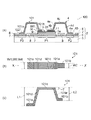
まず、本発明の第1実施形態に係る半導体装置の実装構造について、図1乃至図4を参照して説明する。図1(a),(b),(c)に示すように、半導体装置の実装構造1は、配線基板2と、半導体装置3と、接続部材4とから構成されている。
(First embodiment)
First, the mounting structure of the semiconductor device according to the first embodiment of the present invention will be described with reference to FIGS. As shown in FIGS. 1A, 1 </ b> B, and 1 </ b> C, the semiconductor
配線基板2は、基材5と絶縁層6、配線層7、レジスト層8とから構成されている。また、基材5の材質としては、本実施形態ではAlから形成されている。これは、半導体装置3に大電流を流した際に発生する熱を効率よく放熱させるために設けている。なお、本実施形態では基材5の材質はAlであるが、これに限られることはなく、例えばCu等の放熱性の高い金属や、AlNやSi3N4等の放熱性の高いセラミックから形成されていれば良い。また、セラミックから形成されている場合、絶縁性が確保出来るため、絶縁層6が不要となる。
The
絶縁層6は、基材5を覆うように設けられており、基材5と後述する配線層7との導通を防ぐために設けられている。また、絶縁層6の材質としては絶縁性の樹脂、あるいは絶縁性の樹脂内に、例えばSiO2やAl2O3等の放熱性の高い粒子を含むものから形成されている。
The
配線層7は、絶縁層6上の所定の位置に設けられており、配線層7の端部には、半導体装置3及び接続部材4と接続するための第1,第2のパッド部P1,P2が形成されている。また、配線層7の第1のパッド部P1の面積は、半導体装置3の第1の電極3aの面積と同等又は大きい面積に形成されており、第2のパッド部P2の面積は、後述する接続部材4の第1の接合部材4aの面積と同等又は大きい面積となるように形成されている。
The
配線層7の材質としては、本実施形態ではCuから形成されているが、これに限られることはなく、導電性の金属であればよい。
The material of the
レジスト層8は、配線層7の第1,第2のパッド部P1,P2から一定の間隔を設けて囲むように、絶縁層6と配線層7上に形成されている。また、レジスト層8の材質としては、絶縁性の樹脂から形成されている。なお、本実施形態では第1,第2のパッド部P1,P2から一定の間隔を設けて囲むようにレジスト層8が形成されているが、これに限られることはなく、例えば図2(a),(b),(c)に示すように、間隔を設けずに第1,第2のパッド部P1,P2を囲むように設けても良く、また、図3に示すように配線層7の一部を覆うように形成されていてもよい。
The
半導体装置3は、一方の面に第1の電極3aが形成され、他方の面に第2の電極3bが形成されており、お互いが対向するように設けられている。また、半導体装置3は、半導体装置3の第1の電極3aと、配線層7の第1のパッド部P1とを第1の接合材9を介して接続するように設けている。接続の為に用いている第1の接合材9の材質としては、本実施形態では半田を使用しているが、これに限られることはなく、例えばAgペースト等の導電性の材質であればよい。
The
このように、配線基板2の第1のパッド部P1上に第1の接合材9を介して半導体装置3を設けることにより、従来の半導体パッケージのリードフレームの厚みや、接続部材まで覆うように封止している樹脂の厚みの分だけ薄くすることが可能となる。また、リードフレームのリード端子の長さを配慮して実装面積を確保する必要がないため、より省スペースに半導体装置3を実装することが可能となる。
As described above, by providing the
更に、配線基板2と半導体装置3を第1の接合材9を介して設けていることにより、大電流を流した際に半導体装置3から発生する熱を、効率よく配線基板2へと放熱することが可能となる。その結果、半導体装置3の寿命を伸ばす事ができる。
Further, by providing the
接続部材4は、第2の接合材10と接する第1の接合部材4aと、第3の接合材11と接する第2の接合部材4bと、第1の接合部材4aと第2の接合部材4bと一定の間隔を設けて形成されている第1の部材4cと、第1の部材4cを支持し、第1の接合部材4aと接続している第2の部材4dと、第1の部材4cを支持し、第2の接合部材4bと接続している第3の部材4eとから構成されている。
The connecting member 4 includes a
より詳しく説明すると、接続部材4の幅Wは、第1,第2の接合部材4a,4bの幅とほぼ同じ幅となるように形成されており、半導体装置3の第2の電極3bや第2のパッド部P2に対して同じ幅、もしくは少し狭くなるように形成されている。なお、本実施形態では接続部材4の幅Wが第1,第2の接合部材4a,4bの幅とほぼ同じ幅となるように形成されているが、異なる幅となるように形成されていてもよい。また、第1,第2の接続部材4a,4bの幅が異なる幅となるように形成されていてもよい。
More specifically, the width W of the connection member 4 is formed to be substantially the same as the width of the first and
また、図4に示すように、接続部材4は、板状のCuから形成されており、厚みTが約0.1mm〜0.3mmのものを用いている。そして、第3の部材4eの長さL2が、厚みTより0.2mm以上長くなるように形成されている。すなわち、第1の部材4cと第2の接合部材4bの厚みの合計に、更に0.2mm以上を加えた長さとなるように形成されており、本実施形態では約0.4mm以上となるように形成されている。また、第2の部材4dの長さL1は、第1の部材4cが配線基板2に略平行となるような高さに調整されている。
As shown in FIG. 4, the connecting member 4 is made of plate-like Cu and has a thickness T of about 0.1 mm to 0.3 mm. The length L2 of the
この様に、第3の部材4eの長さL2が約0.4mm以上のものを用いている理由としては、第3の接合材11と第2の接合部材4bの接続信頼性を確保するためである。
As described above, the reason why the length L2 of the
配線基板2の基材5や半導体装置3、接続部材4は、半導体装置3に大電流を流した際に発生する熱や、周囲の環境温度の差により膨張するのだが、それぞれの熱膨張係数が異なるため、接続部材4と半導体装置3を接続する第3の接合材11や、基材5と接続部材4を接続する第2,第3の接合材10,11に応力がかかりやすくなる。また、この応力は、第2,第3の部材4d,4eの長さL1,L2が短いほど応力が集中しやすくなり、特に第3の部材4eの長さL2を約0.4mm未満の長さに形成すると破断しやすくなる。そのため、第3の部材4eの長さL2を約0.4mm以上となるように形成することで、応力を分散させ、破断を防いでいる。
The
次に、本発明の第1実施形態に係る半導体装置の実装方法について図5を参照して説明する。 Next, a semiconductor device mounting method according to the first embodiment of the present invention will be described with reference to FIG.
まず、図5(a)に示すように、基材5上に絶縁層6が形成され、絶縁層6上の一部に形成されている配線層7と、第1,第2のパッド部P1,P2を一定の間隔を設けて囲むように絶縁層6と配線層7上に形成されているレジスト層8とを有する配線基板2を用意し、第1のパッド部P1と第2のパッド部P2それぞれに第1の接合材9、第2の接合材10を設ける。また、第1,第2の接合材9,10は、本実施形態ではスクリーン印刷により設けているが、これに限られることはなく、一括で形成する事が可能であればどの様な方法でも良い。
First, as shown in FIG. 5A, the insulating
次に、図5(b)に示すように、第1の接合材9上に、半導体装置3の第1の電極3aが接するように設ける。そして、図5(c)に示すように、半導体装置3の第2の電極3b上に第3の接合材11を設ける。本実施形態では、第3の接合材11はディスペンサを使用して設けているが、これに限られることは無く、例えば転写等、第3の接合材11を設けることが出来ればどの様な方法でも良い。
Next, as shown in FIG. 5B, the
その後、図5(d)に示すように、接続部材4の第1の接合部材4aと第2の接合部材4bとをそれぞれ第2の接合材10と第3の接合材11に接するように設け、加熱装置12により加熱を行う。これにより、図1(a),(b),(c)に示すような半導体装置の実装構造1となる。
After that, as shown in FIG. 5D, the
以上、第1実施形態の半導体装置の実装構造1によれば、配線基板2の第1のパッド部P1上に第1の接合材9を介して半導体装置3を設けている。これにより、小型化して実装することが可能となるため、より省スペースで半導体装置3を設けることができる。
As described above, according to the semiconductor
更に、半導体装置3から発生する熱を、効率よく配線基板2へと放熱することが可能となり、その結果、半導体装置3の寿命を伸ばす事ができる。
Furthermore, it is possible to efficiently dissipate heat generated from the
なお、本実施形態の半導体装置の実装構造1では、半導体チップ3に対して1つの接続部材4を設けているが、これに限られることはなく、図6(a)に示す半導体装置の実装構造100のように、第1の接続部材(接続部材)4と第2の接続部材(接続部材)101を設けてもよい。
In the semiconductor
すなわち、第3のパッド部P3と、半導体装置3の第3の電極3cが形成されている配線基板2上に、第4の接合材102と第5の接合材103がそれぞれ設けられている。そして、第2の接続部材101の第1の接合部材101aは第4の接合材102と接するように設けられ、第2の接続部材101の第2の接合部材101bは第5の接合材103と接するように設けられている。
That is, the
また、図6(b),(c)に示すように、第2の接続部材(接続部材)101は、第1の接合部材101aの幅W1と、第1,第2の部材101c,101dの幅W3,W4が同じ幅となるように形成されており、第2の接合部材101bの幅W2より広くなるように形成されている。そして、第3の部材101eは第2の接合部材101bから第1の部材101cに向かって、次第に広くなるように形成されている。
Further, as shown in FIGS. 6B and 6C, the second connecting member (connecting member) 101 includes the width W1 of the first joining
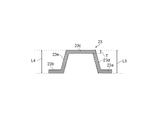
第2の接続部材(接続部材)101の厚みTは、約0.2mmであり、第1の接合部材101aの幅W1と第1,第2の部材101c,101dの幅W3,W4は約2.2mm、第2の接合部材101bの幅W2が約1.5mmとなるように形成されている。そして、第2の部材101dの長さL1が約1.45mm、第3の部材101eの長さL2が約1.15mmの長さとなるように形成されている。
The thickness T of the second connecting member (connecting member) 101 is about 0.2 mm, and the width W1 of the first joining
また、この他に図7に示す半導体装置の実装構造200ように、絶縁層6、配線層7、レジスト層8の一部と、半導体装置3の一部と、接続部材4の第2の接合部材4b、第3の部材4eの一部を覆うように樹脂201を設けても良い。このように形成することにより、例えば低温の環境では、樹脂201が収縮することで、半導体装置3と接続部材4へと圧縮する力が働くため、第3の接合材11に生じるクラックの発生を抑制することができる。その結果、接続信頼性を確保することが可能となる。
In addition to this, as in the semiconductor
(第2実施形態)
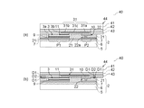
次に、本発明の第2実施形態に係る半導体装置の実装構造について、図8、図9を参照して説明する。本実施形態の半導体装置の実装構造20は、絶縁材21に配線22が形成されている点と、接続部材23の第2の部材23dの長さL3と第3の部材23eの長さL4が同じである点で第1実施形態と異なり、その他の構成部分については、同様の構成を有している。従って、図8(a),(b),(c)及び図9では、第1実施形態と異なる配線22が形成されている絶縁材21と、接続部材23を示し、以下の説明においては、第1実施形態と同様の構成部分については、詳細説明を省略して異なる構成部分についてのみ説明する。
(Second Embodiment)
Next, a semiconductor device mounting structure according to a second embodiment of the present invention will be described with reference to FIGS. In the mounting
絶縁材21は、第2の接合材10と第3の接合材11を設ける位置がほぼ同じ位置となるような厚みに形成されており、第2のパッド部P2と、第2の接合材10とを電気的に接続させるためにビア22aが形成されている。また、ビア22a内にはCuのめっきが形成されている。なお、本実施形態ではビア22aにCuのめっきが設けられているがこれに限られることはなく、導電性のペーストの充填等、導電性の金属が形成されていればよい。
The insulating
また、絶縁材21は、第1のパッド部P1から一定の間隔を設けて囲むように、絶縁層6と配線層7上に形成されている。そのため、第1のパッド部P1と接続する配線層7の一部が露出する。なお、本実施形態では、第1のパッド部P1から一定の間隔を設けて囲むように絶縁材21を設けているが、これに限られることはなく、一定の間隔無く囲むように絶縁材21を設けてもよく、また、配線層7の一部を覆うように形成されていてもよい。
In addition, the insulating
このように絶縁材21を、第2の接合材10と第3の接合材11を設ける位置がほぼ同じとなるような厚みに形成することにより、例えばスクリーン印刷等で第2,第3の接合材10,11を一括で設けることができるようになる。そして、第3の接合材11の供給量を安定化させることができる。
In this way, the insulating
これは、例えばディスペンサ等により部分的に第2,第3の接合材10,11を供給する場合、第1の接合材9を供給する場合に比べて供給量が少ないため、バラつきが生じやすくなる。そのため、高い精度で第2,第3の接合材10,11を設けなければならない。本実施形態の絶縁材21を形成することにより、例えばスクリーン印刷等のバラつきの少ない方法で第2,第3の接合材10,11を設けることができるので、供給量を安定化させ、半導体装置3と接続部材4の接続信頼性を更に確保することが可能となる。
This is because, for example, when the second and
接続部材23は、第2の接合材10と接する第1の接合部材23aと、第3の接合材11と接する第2の接合部材23bと、第1の接合部材23aと第2の接合部材23bと一定の間隔を設けて形成されている第1の部材23cと、第1の部材23cを支持し、第1の接合部材23aと接続している第2の部材23dと、第1の部材23cを支持し、第2の接合部材23bと接続している第3の部材23eとから構成されている。
The
また、接続部材23は、絶縁材21の厚みの変更に伴い、接続部材23の第1の部材23cが配線基板2に対して略平行となるようにするため、図9に示すように第2の部材23dの長さL3と第3の部材23eの長さL4とがほぼ同じとなるように形成されている。
Further, the
次に、本発明の第2実施形態に係る半導体装置の実装方法について図10を参照して説明する。 Next, a semiconductor device mounting method according to the second embodiment of the present invention will be described with reference to FIG.
まず、図10(a)に示すように、第1のパッド部P1上に第1の接合材9を設ける。より詳しく説明すると、基材5上に絶縁層6、第1,第2のパッド部P1,P2を含む配線層7、第2のパッド部P2と電気的に接続可能に設けられた配線22が形成された絶縁材21から形成されている配線基板2を用意し、第1のパッド部P1上に例えばディスペンサ等を用いて第1の接合材9を設ける。
First, as shown in FIG. 10A, the
なお、本実施形態では、第1の接合材9をディスペンサにて設けているが、これに限られることはなく、設ける事が可能であればどのような方法でもよい。
In the present embodiment, the
次に、図10(b)に示すように、第1の接合材9上に、半導体装置3の第1の電極3aが接するように設ける。そして、図10(c)に示すように、半導体装置3の第2の電極3bと配線22上に第2,第3の接合材10,11を設ける。本実施形態では、第2,第3の接合材10,11をスクリーン印刷により一括で設けているが、これに限られることは無く、第2,第3の接合材10,11を安定的に供給することが出来ればどの様な方法でも良い。また、第1の接合材9上に半導体装置3を設けた後、半導体装置3の第2の電極3bと配線22に第2,第3の接合材10,11を設けているが、半導体装置3と第1の接合材9を接合させるために、リフロー等により加熱する工程を入れてもよい。これにより、第2,第3の接合材10,11を設ける際に、半導体装置3の位置ズレを抑制することが可能となる。
Next, as shown in FIG. 10B, the
その後、図10(d)に示すように、接続部材23の第1の接合部材23aと第2の接合部材23bとをそれぞれ第2の接合材10と第3の接合材11に接するように設け、加熱装置12により加熱を行う。これにより、図8(a),(b),(c)に示すような半導体装置の実装構造20となる。
Thereafter, as shown in FIG. 10 (d), the
以上、第2実施形態の半導体装置の実装構造20によれば、配線基板2の第1のパッド部P1上に第1の接合材9を介して半導体装置3を設けることにより、小型化して実装することが可能となるため、より省スペースで半導体装置3を設けることができる。
As described above, according to the semiconductor
また、半導体装置3から発生する熱を、効率よく配線基板2へと放熱することが可能となり、その結果、半導体装置3の寿命を伸ばす事ができる。
Further, the heat generated from the
更に、絶縁材21を、第2の接合材10と第3の接合材11を設ける位置がほぼ同じとなるような厚みに形成することにより、第3の接合材11の供給量を安定化させることができ、接続部材23との接続信頼性を確保することが可能となる。
Furthermore, the supply amount of the
本発明のいくつかの実施形態を説明したが、これらの実施形態は、例として提示したものであり、発明の範囲を限定することは意図していない。これら新規な実施形態は、その他のさまざまな形態で実施されることが可能であり、発明の要旨を逸脱しない範囲で、種々の省略、置き換え、変更を行うことができる。これら実施形態やその変形は、発明の範囲や要旨に含まれるとともに、特許請求の範囲に記載された発明とその均等の範囲に含まれる。 Although several embodiments of the present invention have been described, these embodiments are presented by way of example and are not intended to limit the scope of the invention. These novel embodiments can be implemented in various other forms, and various omissions, replacements, and changes can be made without departing from the scope of the invention. These embodiments and modifications thereof are included in the scope and gist of the invention, and are included in the invention described in the claims and the equivalents thereof.
例えば、図11に示す半導体装置の実装構造30のように、接続部材31が板状形状であってもよい。より詳しく説明すると、第2の接合材10と接する第1の接合部材31aと、第3の接合材11と接する領域である第2の接合部材31bと、第1の接合部材31aと第2の接合部材31bと同じ高さで接続している接合部材接続部31cとで構成されている。この場合、接続部材31を設けるためのスペースを減少させることが出来るため、更に小スペースで半導体装置3を設けることができる。
For example, the
また、図11のような構造にすることで、図12(a)に示すような半導体装置の実装構造40を形成することが可能となる。この半導体装置の実装構造40は、例えばCuやAl等の金属から形成されている基材41上に絶縁層42を設け、更にその上に接続部材31と、接続部材31の第1,第2の接合部材31a,31bを囲み、露出するように接続部材31と絶縁層42上に設けられたレジスト層43が形成された接続部材付配線基板44を用いて、第2,第3の接合材10,11と第1,第2の接合部材31a,31bとが接するような構造となっている。
Further, by adopting the structure as shown in FIG. 11, it is possible to form the semiconductor
なお、基材41は、例えばCuやAl等の金属から形成されたものを用いているが、これに限られることはなく、AlNやSi3N4等の放熱性の高いセラミックから形成されていても良い。また、セラミックから形成されている場合、絶縁性が確保出来るため、絶縁層42が不要となる。
Incidentally, the
これにより、省スペースな実装だけでなく、半導体装置3から放熱される熱を接続部材付配線基板44から効率よく放熱させることが出来る。
Thereby, not only the space-saving mounting, but also the heat radiated from the
また、図12(b)に示すように、配線基板2の絶縁材21の一部と、向かい合う接続部材付配線基板44のレジスト層43の一部にダミー配線D1を形成し、ダミー接続部材D2を介して接続する構造にしてもよい。これにより、接続部材31と半導体装置3の接続信頼性を確保することができる。
Further, as shown in FIG. 12B, a dummy wiring D1 is formed on a part of the insulating
1,20,30,40,100,200…半導体装置の実装構造
2…配線基板
3…半導体装置
3a…第1の電極
3b…第2の電極
3c…第3の電極
4,23,31,101…接続部材
4a,23a,31a,101a…第1の接合部材
4b,23b,31b,101b…第2の接合部材
4c,23c…第1の部材
4d,23d…第2の部材
4e,23e…第3の部材
31c…接合部材接続部
5,41…基材
6,42…絶縁層
7…配線層
8,43…レジスト層
9…第1の接合材
10…第2の接合材
11…第3の接合材
12…加熱装置
21…絶縁材
22…配線
22a…ビア
44…接続部材付配線基板
102…第4の接合材
103…第5の接合材
201…樹脂
P1…第1のパッド部
P2…第2のパッド部
P3…第3のパッド部
D1…ダミー配線
D2…ダミー接続部材
W…幅
T…厚み
L1,L3…第2の部材の長さ
L2,L4…第3の部材の長さ
DESCRIPTION OF
Claims (10)
前記複数のパッド部の一方の上に電気的に接続するように設けられている半導体装置と、
前記複数のパッド部の他方の上に設けられている接合材と、
前記半導体装置の上に設けられている接合材と、
前記複数のパッド部の他方の上に設けられている接合材と、前記半導体装置の上に設けられている接合材と、に接するように設けられている接続部材と、
を有し、
前記接続部材は、前記複数のパッド部の他方の上に設けられている接合材と接する第1の接合部材と、
前記半導体装置の上に設けられている接合材と接する第2の接合部材と、
前記第1の接合部材と前記第2の接合部材と一定の間隔を設けて形成されている第1の部材と、
前記第1の部材を支持し、前記第1の接合部材と接続している第2の部材と、
前記第1の部材を支持し、前記第2の接合部材と接続し、0.4mm以上1.15mm以下の長さに設けられている第3の部材と、
を有することを特徴とする半導体装置の実装構造。 A wiring board having a wiring layer formed on a part of the substrate, and a resist layer formed so as to surround a plurality of pad portions that are a part of the wiring layer;
A semiconductor device provided to be electrically connected to one of the plurality of pad portions;
A bonding material provided on the other of the plurality of pad portions;
A bonding material provided on the semiconductor device;
A connecting member provided to be in contact with a bonding material provided on the other of the plurality of pad portions and a bonding material provided on the semiconductor device;
Have
The connection member includes a first bonding member that contacts a bonding material provided on the other of the plurality of pad portions;
A second bonding member in contact with a bonding material provided on the semiconductor device;
A first member formed at a certain interval from the first joining member and the second joining member;
A second member supporting the first member and connected to the first joining member;
A third member that supports the first member, is connected to the second joining member, and is provided with a length of 0.4 mm or more and 1.15 mm or less;
A mounting structure of a semiconductor device, comprising:
基材上の一部に形成されている配線層と、前記配線層の一部である複数のパッド部を囲むように形成されているレジスト層と、を有する配線基板と、前記複数のパッド部の一方の上に電気的に接続するように半導体装置を設ける工程と、
前記複数のパッド部の他方の上と、前記半導体装置の上に接合材を設ける工程と、
前記複数のパッド部の他方の上に設けられている接合材と、前記半導体装置の上に設けられている接合材と、に接するように接続部材を設ける工程と、
を有することを特徴とする半導体装置の実装方法。 A semiconductor device mounting method for forming a semiconductor device mounting structure according to any one of claims 1 to 8,
A wiring board having a wiring layer formed on a part of a substrate, and a resist layer formed so as to surround a plurality of pad parts that are a part of the wiring layer, and the plurality of pad parts Providing a semiconductor device so as to be electrically connected on one of
Providing a bonding material on the other of the plurality of pad portions and on the semiconductor device;
Providing a connecting member so as to contact the bonding material provided on the other of the plurality of pad portions and the bonding material provided on the semiconductor device;
A method for mounting a semiconductor device, comprising:
Priority Applications (1)
| Application Number | Priority Date | Filing Date | Title |
|---|---|---|---|
| JP2011076410A JP6043049B2 (en) | 2011-03-30 | 2011-03-30 | Semiconductor device mounting structure and semiconductor device mounting method |
Applications Claiming Priority (1)
| Application Number | Priority Date | Filing Date | Title |
|---|---|---|---|
| JP2011076410A JP6043049B2 (en) | 2011-03-30 | 2011-03-30 | Semiconductor device mounting structure and semiconductor device mounting method |
Publications (3)
| Publication Number | Publication Date |
|---|---|
| JP2012212712A JP2012212712A (en) | 2012-11-01 |
| JP2012212712A5 JP2012212712A5 (en) | 2014-04-24 |
| JP6043049B2 true JP6043049B2 (en) | 2016-12-14 |
Family
ID=47266464
Family Applications (1)
| Application Number | Title | Priority Date | Filing Date |
|---|---|---|---|
| JP2011076410A Active JP6043049B2 (en) | 2011-03-30 | 2011-03-30 | Semiconductor device mounting structure and semiconductor device mounting method |
Country Status (1)
| Country | Link |
|---|---|
| JP (1) | JP6043049B2 (en) |
Families Citing this family (6)
| Publication number | Priority date | Publication date | Assignee | Title |
|---|---|---|---|---|
| EP2858100B1 (en) * | 2012-05-29 | 2020-06-10 | NSK Ltd. | Semiconductor module and production method for same |
| CN103918076B (en) * | 2012-11-05 | 2016-11-16 | 日本精工株式会社 | Semiconductor module |
| US9609775B2 (en) | 2012-11-05 | 2017-03-28 | Nsk Ltd. | Semiconductor module |
| CN103918066B (en) | 2012-11-05 | 2016-08-24 | 日本精工株式会社 | Semiconductor module |
| CN108565254B (en) * | 2013-10-21 | 2021-08-24 | 日本精工株式会社 | Semiconductor module |
| JP6566634B2 (en) * | 2014-12-09 | 2019-08-28 | 国立大学法人大阪大学 | Junction structure and manufacturing method of junction structure |
Family Cites Families (7)
| Publication number | Priority date | Publication date | Assignee | Title |
|---|---|---|---|---|
| JP4550503B2 (en) * | 2004-07-22 | 2010-09-22 | ルネサスエレクトロニクス株式会社 | Semiconductor device |
| JP2006344652A (en) * | 2005-06-07 | 2006-12-21 | Toshiba Components Co Ltd | Semiconductor device and method of mounting semiconductor component |
| JP5076440B2 (en) * | 2006-10-16 | 2012-11-21 | 富士電機株式会社 | Semiconductor device and manufacturing method of semiconductor device |
| JP2010050364A (en) * | 2008-08-25 | 2010-03-04 | Hitachi Ltd | Semiconductor device |
| JP5388661B2 (en) * | 2009-04-03 | 2014-01-15 | 三菱電機株式会社 | Semiconductor device and manufacturing method thereof |
| JP2012212713A (en) * | 2011-03-30 | 2012-11-01 | Toshiba Corp | Mounting structure of semiconductor device |
| JP2012217213A (en) * | 2012-08-01 | 2012-11-08 | Toshiba Corp | Image processing device and image processing method |
-
2011
- 2011-03-30 JP JP2011076410A patent/JP6043049B2/en active Active
Also Published As
| Publication number | Publication date |
|---|---|
| JP2012212712A (en) | 2012-11-01 |
Similar Documents
| Publication | Publication Date | Title |
|---|---|---|
| US6972479B2 (en) | Package with stacked substrates | |
| JP6043049B2 (en) | Semiconductor device mounting structure and semiconductor device mounting method | |
| JP2012212713A (en) | Mounting structure of semiconductor device | |
| JP5776701B2 (en) | Semiconductor device and method for manufacturing semiconductor device | |
| JP6012533B2 (en) | Power semiconductor device | |
| JP2006196709A (en) | Semiconductor device and manufacturing method thereof | |
| JP5589950B2 (en) | Electronic equipment | |
| JP2007142097A (en) | Semiconductor device | |
| JP5214121B2 (en) | Light emitting device | |
| JP2008085002A (en) | Semiconductor device and its manufacturing method | |
| JP2006261293A (en) | Semiconductor device and insulation substrate for use thereof | |
| JP4556732B2 (en) | Semiconductor device and manufacturing method thereof | |
| CN211182196U (en) | Lead frame, semiconductor device, and circuit device | |
| JP2007012718A (en) | Electronic component housing package and electronic device | |
| JP7310161B2 (en) | Semiconductor device and its manufacturing method | |
| JP2009164511A (en) | Semiconductor device and method of manufacturing the same | |
| JP5217013B2 (en) | Power conversion device and manufacturing method thereof | |
| JP5145168B2 (en) | Semiconductor device | |
| JP5124329B2 (en) | Semiconductor device | |
| JP5217014B2 (en) | Power conversion device and manufacturing method thereof | |
| CN110931448A (en) | Lead frame, semiconductor device, and circuit device | |
| JP2009158825A (en) | Semiconductor device | |
| JP2007201251A (en) | Semiconductor package, and manufacturing method thereof | |
| JP2006344652A (en) | Semiconductor device and method of mounting semiconductor component | |
| JP2007305911A (en) | Semiconductor package and semiconductor module |
Legal Events
| Date | Code | Title | Description |
|---|---|---|---|
| A521 | Request for written amendment filed |
Free format text: JAPANESE INTERMEDIATE CODE: A523 Effective date: 20140310 |
|
| A621 | Written request for application examination |
Free format text: JAPANESE INTERMEDIATE CODE: A621 Effective date: 20140310 |
|
| A131 | Notification of reasons for refusal |
Free format text: JAPANESE INTERMEDIATE CODE: A131 Effective date: 20150213 |
|
| RD02 | Notification of acceptance of power of attorney |
Free format text: JAPANESE INTERMEDIATE CODE: A7422 Effective date: 20150216 |
|
| RD04 | Notification of resignation of power of attorney |
Free format text: JAPANESE INTERMEDIATE CODE: A7424 Effective date: 20150218 |
|
| A977 | Report on retrieval |
Free format text: JAPANESE INTERMEDIATE CODE: A971007 Effective date: 20150219 |
|
| A521 | Request for written amendment filed |
Free format text: JAPANESE INTERMEDIATE CODE: A523 Effective date: 20150414 |
|
| A131 | Notification of reasons for refusal |
Free format text: JAPANESE INTERMEDIATE CODE: A131 Effective date: 20151127 |
|
| A521 | Request for written amendment filed |
Free format text: JAPANESE INTERMEDIATE CODE: A523 Effective date: 20160126 |
|
| A131 | Notification of reasons for refusal |
Free format text: JAPANESE INTERMEDIATE CODE: A131 Effective date: 20160729 |
|
| A521 | Request for written amendment filed |
Free format text: JAPANESE INTERMEDIATE CODE: A523 Effective date: 20160920 |
|
| TRDD | Decision of grant or rejection written | ||
| A01 | Written decision to grant a patent or to grant a registration (utility model) |
Free format text: JAPANESE INTERMEDIATE CODE: A01 Effective date: 20161014 |
|
| A61 | First payment of annual fees (during grant procedure) |
Free format text: JAPANESE INTERMEDIATE CODE: A61 Effective date: 20161111 |
|
| R151 | Written notification of patent or utility model registration |
Ref document number: 6043049 Country of ref document: JP Free format text: JAPANESE INTERMEDIATE CODE: R151 |