JP2006324324A - Light emitting device, method for manufacturing light emitting device, and nitride semiconductor substrate - Google Patents
Light emitting device, method for manufacturing light emitting device, and nitride semiconductor substrate Download PDFInfo
- Publication number
- JP2006324324A JP2006324324A JP2005144110A JP2005144110A JP2006324324A JP 2006324324 A JP2006324324 A JP 2006324324A JP 2005144110 A JP2005144110 A JP 2005144110A JP 2005144110 A JP2005144110 A JP 2005144110A JP 2006324324 A JP2006324324 A JP 2006324324A
- Authority
- JP
- Japan
- Prior art keywords
- emitting device
- nitride semiconductor
- light emitting
- light
- layer
- Prior art date
- Legal status (The legal status is an assumption and is not a legal conclusion. Google has not performed a legal analysis and makes no representation as to the accuracy of the status listed.)
- Pending
Links
Images


Classifications
-
- H—ELECTRICITY
- H10—SEMICONDUCTOR DEVICES; ELECTRIC SOLID-STATE DEVICES NOT OTHERWISE PROVIDED FOR
- H10H—INORGANIC LIGHT-EMITTING SEMICONDUCTOR DEVICES HAVING POTENTIAL BARRIERS
- H10H20/00—Individual inorganic light-emitting semiconductor devices having potential barriers, e.g. light-emitting diodes [LED]
- H10H20/80—Constructional details
- H10H20/81—Bodies
- H10H20/819—Bodies characterised by their shape, e.g. curved or truncated substrates
-
- H—ELECTRICITY
- H10—SEMICONDUCTOR DEVICES; ELECTRIC SOLID-STATE DEVICES NOT OTHERWISE PROVIDED FOR
- H10H—INORGANIC LIGHT-EMITTING SEMICONDUCTOR DEVICES HAVING POTENTIAL BARRIERS
- H10H20/00—Individual inorganic light-emitting semiconductor devices having potential barriers, e.g. light-emitting diodes [LED]
- H10H20/80—Constructional details
- H10H20/81—Bodies
- H10H20/822—Materials of the light-emitting regions
- H10H20/824—Materials of the light-emitting regions comprising only Group III-V materials, e.g. GaP
- H10H20/825—Materials of the light-emitting regions comprising only Group III-V materials, e.g. GaP containing nitrogen, e.g. GaN
-
- H—ELECTRICITY
- H10—SEMICONDUCTOR DEVICES; ELECTRIC SOLID-STATE DEVICES NOT OTHERWISE PROVIDED FOR
- H10W—GENERIC PACKAGES, INTERCONNECTIONS, CONNECTORS OR OTHER CONSTRUCTIONAL DETAILS OF DEVICES COVERED BY CLASS H10
- H10W72/00—Interconnections or connectors in packages
- H10W72/851—Dispositions of multiple connectors or interconnections
- H10W72/874—On different surfaces
- H10W72/884—Die-attach connectors and bond wires
Landscapes
- Led Devices (AREA)
- Drying Of Semiconductors (AREA)
- Led Device Packages (AREA)
Abstract
【課題】 製造コストを増大させることなく光の取出し効率を向上させることが可能な発光装置、当該発光装置の製造方法および当該発光装置の製造に用いることができる窒化物半導体基板を提供する。
【解決手段】 この発明に従った発光装置は、GaN基板1と、GaN基板1の第1の主表面の側に、n型AlxGa1-xN層3と、GaN基板1から見てn型AlxGa1-xN層3より遠くに位置するp型AlxGa1-xN層5と、n型AlxGa1-xN層3およびp型AlxGa1-xN層5の間に位置する量子井戸(MQW:Multi-Quantum Well)4とを備えた発光装置である。当該発光装置では、p型AlxGa1-xN層5の側をダウン実装し、GaN基板1の第1の主表面と反対側の主表面である第2の主表面1aから光を放出する。GaN基板1の第2の主表面1aには半球状の凸部82が形成されている。
【選択図】 図1PROBLEM TO BE SOLVED: To provide a light emitting device capable of improving light extraction efficiency without increasing the manufacturing cost, a method for manufacturing the light emitting device, and a nitride semiconductor substrate that can be used for manufacturing the light emitting device.
A light-emitting device according to the present invention is viewed from a GaN substrate 1, an n-type Al x Ga 1-x N layer 3 and a GaN substrate 1 on the first main surface side of the GaN substrate 1. n-type Al x Ga 1-x and p-type Al x Ga 1-x n layer 5 positioned far from the n layer 3, n-type Al x Ga 1-x n layer 3 and p-type Al x Ga 1-x n The light emitting device includes a quantum well (MQW) 4 positioned between the layers 5. In the light emitting device, the p-type Al x Ga 1-x N layer 5 side is down-mounted, and light is emitted from the second main surface 1a which is the main surface opposite to the first main surface of the GaN substrate 1. To do. A hemispherical convex portion 82 is formed on the second main surface 1 a of the GaN substrate 1.
[Selection] Figure 1
Description
本発明は、発光装置、発光装置の製造方法および窒化物半導体基板に関し、より具体的には窒化物半導体から形成される発光装置、発光装置の製造方法および窒化物半導体基板に関するものである。なお、本発明における発光装置とは、窒化物半導体基板とその上に積層された半導体層とを主体に形成される半導体素子または半導体チップのみを指す場合もあるし、また、半導体チップが実装部品に搭載され樹脂封止されたデバイスのみを指す場合もある。さらに、両方の意味に用いられる場合もある。また、半導体チップを単にチップと呼ぶ場合がある。また、チップのうち基板とその上に形成されたエピタキシャル層とを、単に基板と呼ぶ場合がある。 The present invention relates to a light emitting device, a method for manufacturing a light emitting device, and a nitride semiconductor substrate, and more specifically to a light emitting device formed from a nitride semiconductor, a method for manufacturing a light emitting device, and a nitride semiconductor substrate. The light emitting device in the present invention may refer only to a semiconductor element or a semiconductor chip mainly formed of a nitride semiconductor substrate and a semiconductor layer stacked thereon, or the semiconductor chip may be a mounting component. In some cases, it refers only to a device mounted on and sealed with resin. Furthermore, it may be used for both meanings. A semiconductor chip may be simply called a chip. Further, the substrate and the epitaxial layer formed thereon may be simply referred to as a substrate.
白色発光ダイオード(LED:Light Emitting Diode)は、今のところ携帯情報端末などの小型電子機器の照明に盛んに用いられているが、今後、大きな空間または大面積の照明に用いられる可能性を秘めている。大空間、大面積の照明に用いられるためには、LEDの光の出力を大きくする必要がある。 White light emitting diodes (LEDs) are currently actively used for lighting small electronic devices such as personal digital assistants, but have the potential to be used for lighting in large spaces or large areas in the future. ing. In order to be used for illumination in a large space and a large area, it is necessary to increase the light output of the LED.
このようにLEDの光の出力を大きくするための方策の1つとして、LEDの内部で発生した光を効率的に外部に出力させること、すなわち光の取出し効率の向上が上げられる。このような光の取出し効率を向上させる技術として、従来、サファイアなどからなる基板において窒化物半導体層の積層される面と反対側の裏面にて、ブラスト加工により凹凸形状の光の反射面を形成した発光装置(たとえば、特許文献1参照)、サファイアなどからなる基板の上記裏面において、溝の形成と研磨とを組合せることによりレンズ効果を有する曲面形状を形成した発光装置(たとえば、特許文献2参照)、さらに、サファイア基板上に積層された窒化ガリウム(GaN)デバイスであって、n−GaN層上に電極が形成されるとともに、n−GaN層表面がエッチングされることにより当該n−GaN層表面に0.5〜1μmの直径の半球状の凸部が形成されたデバイス(たとえば、非特許文献1参照)などが提案されている。
上述した特許文献1に開示された発光装置では、ブラスト加工により凹凸形状を形成しているが、このような加工方法では凹凸形状部の形状を正確に制御することは困難である。また、上記特許文献1には反射面を形成する方法としてダイサー加工やレーザー加工も例示されているが、このような加工方法によりたとえば半球状の曲面を形成することは難しい。
In the light emitting device disclosed in
また、上記特許文献2では、ダイサー加工やレーザー加工により溝を形成した後研磨を行なうことにより曲面形状を形成するとしているが、この場合にはダイサー加工などと研磨加工とを組合せているので、単純なダイサー加工のみの場合などと比較すると製造工程数が増えることになる。このため、発光装置の製造コストが増大することになっていた。
Further, in
また、非特許文献1では、サファイア基板上に積層されたGaN層(n−GaN層)の表面に、エッチングにより半球状の凸部を形成しているので、形成される凸部の直径が積層されたGaN層の厚みに制限される。つまり、より直径の大きな凸部を形成するためには、GaN層を十分厚く積層する必要があるが、このように厚くGaN層を積層するためには積層工程の処理時間が長くなり、結果的に発光装置の製造コストが増大することになる。
Further, in
この発明は、上記のような課題を解決するために成されたものであり、この発明の目的は、製造コストを増大させることなく光の取出し効率を向上させることが可能な発光装置、当該発光装置の製造方法および当該発光装置の製造に用いることができる窒化物半導体基板を提供することである。 The present invention has been made to solve the above-described problems, and an object of the present invention is to provide a light emitting device capable of improving the light extraction efficiency without increasing the manufacturing cost, and the light emission. An object of the present invention is to provide a method for manufacturing a device and a nitride semiconductor substrate that can be used for manufacturing the light emitting device.
この発明に従った発光装置は、窒化物半導体基板と、窒化物半導体基板の第1の主表面の側に、n型窒化物半導体層と、窒化物半導体基板から見てn型窒化物半導体層より遠くに位置するp型窒化物半導体層と、n型窒化物半導体層およびp型窒化物半導体層の間に位置する発光層とを備えた発光装置である。当該発光装置では、p型窒化物半導体層の側をダウン実装し、窒化物半導体基板の第1の主表面と反対側の主表面である第2の主表面から光を放出する。窒化物半導体基板の第2の主表面には半球状の凸部が形成されている。 A light emitting device according to the present invention includes a nitride semiconductor substrate, an n-type nitride semiconductor layer on the first main surface side of the nitride semiconductor substrate, and an n-type nitride semiconductor layer as viewed from the nitride semiconductor substrate. A light-emitting device including a p-type nitride semiconductor layer located farther away and a light-emitting layer located between the n-type nitride semiconductor layer and the p-type nitride semiconductor layer. In the light emitting device, the p-type nitride semiconductor layer side is down-mounted, and light is emitted from the second main surface that is the main surface opposite to the first main surface of the nitride semiconductor substrate. A hemispherical protrusion is formed on the second main surface of the nitride semiconductor substrate.
このようにすれば、窒化物半導体基板の光の出射面である第2の主表面1aに半球状の凸部を形成するので、当該凸部がレンズ効果を奏することにより第2の主表面に垂直な方向に向かう光を効率的に取出すことができる。この結果、凸部が形成されていない場合や、単純に第2の主表面をKOH溶液などを用いて非鏡面化した場合、さらには第2の主表面にダイシングなどを用いて溝を形成した場合より、発光装置における光の利用効率を向上させることができる。
In this way, since the hemispherical convex portion is formed on the second
この発明に従った窒化物半導体基板を備える発光装置の製造方法は、窒化物半導体基板を準備する工程と、半球状の凸部を形成する工程とを備える。半球状の凸部を形成する工程は、窒化物半導体基板において発光層が形成される側である第1の主表面と反対側の第2の主表面に、反応性イオンエッチングを行なうことにより、第2の主表面の一部を除去することによって半球状の凸部を形成する。 A manufacturing method of a light emitting device including a nitride semiconductor substrate according to the present invention includes a step of preparing a nitride semiconductor substrate and a step of forming a hemispherical convex portion. The step of forming the hemispherical protrusion is performed by performing reactive ion etching on the second main surface opposite to the first main surface on the nitride semiconductor substrate on which the light emitting layer is formed, A hemispherical convex portion is formed by removing a part of the second main surface.
このようにすれば、ダイシングや研磨加工などを行なうことなく、反応性イオンエッチングによって上記凸部を形成できる。このため、ダイシングなどを行う場合より発光装置の製造工程を簡略化できる。この結果、本発明による発光装置を低コストで製造できる。 In this way, the convex portion can be formed by reactive ion etching without performing dicing or polishing. For this reason, the manufacturing process of a light-emitting device can be simplified compared with the case where dicing etc. are performed. As a result, the light emitting device according to the present invention can be manufactured at low cost.
この発明に従った窒化物半導体基板は、1つの主表面に半球状の凸部が形成されている。この場合、当該窒化物半導体基板を発光装置の製造に用いて、当該凸部が形成された面を発光装置の光の取出し面とすれば、凸部が形成されていない基板を用いる場合より、光の取出し効率の高い発行装置を製造できる。 The nitride semiconductor substrate according to the present invention has a hemispherical projection on one main surface. In this case, if the nitride semiconductor substrate is used for manufacturing a light-emitting device, and the surface on which the convex portion is formed is a light extraction surface of the light-emitting device, than the case where a substrate on which the convex portion is not formed is used, It is possible to manufacture an issuing device with high light extraction efficiency.
なお、窒化物半導体「基板」は、独立して持ち運びできる厚みが相応に厚い板状物体をさし、持ち運びにおいて単独ではそれ自身の形状を保ち難い「膜」や「層」とは区別される。 Nitride semiconductor “substrate” refers to a plate-like object that can be carried independently, and is distinct from “film” and “layer” that are difficult to maintain by themselves. .
このように、本発明によれば、窒化物半導体基板の第2の主表面に半球状の凸部を形成するので、当該窒化物半導体基板を用いた発光装置における光の取出し効率を向上させることができる。 As described above, according to the present invention, since the hemispherical convex portion is formed on the second main surface of the nitride semiconductor substrate, it is possible to improve the light extraction efficiency in the light emitting device using the nitride semiconductor substrate. Can do.
次に図面を用いて、本発明の実施の形態および実施例について説明する。なお、以下の図面において同一または相当する部分には同一の参照番号を付しその説明は繰返さない。 Next, embodiments and examples of the present invention will be described with reference to the drawings. In the following drawings, the same or corresponding parts are denoted by the same reference numerals, and description thereof will not be repeated.
(実施の形態1)
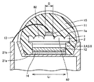
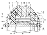
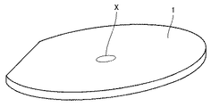
図1は、本発明に従った発光装置としてのLEDの実施の形態1を示す図である。図2は、図1のLEDの発光層を含む積層構造を示す図である。図1および図2を参照して、本発明によるLEDの実施の形態1を説明する。
(Embodiment 1)
FIG. 1 is a
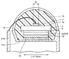
図1に示すように、GaN基板1の第1の主表面の側に後で詳細に説明する発光層などを含む積層構造が形成され、p電極12が設けられている。本実施の形態では、このp電極12が導電性接着剤14によってリードフレームマウント部21aにダウン実装されている。
As shown in FIG. 1, a laminated structure including a light emitting layer, which will be described in detail later, is formed on the first main surface side of the
GaN基板1の第2の主表面1aは、発光層で発光した光を放出する面であり、この面にn電極11が設けられている。この第2の主表面1aには、反応性イオンエッチング(Reactive Ion Etching : RIE)により形成された半球状の凸部82が複数形成されている。n電極11は、第2の主表面全体を覆わないように、第2の主表面1aのほぼ中央部に配置されている。n電極11は、1つの凸部82の頂部を覆うように配置されている。なお、n電極11は1つの凸部82全体を覆うように配置されていてもよく、また複数の凸部82を覆うように配置されていてもよい。ただし、n電極11に被覆されていない部分の比率を大きくとることが重要である。開口率を大きくすれば、n電極11によって遮られる光が減り、光を外に放出する放出効率を高めることができる。
The second
n電極11はワイヤ13によりリードフレームのリード部21bと電気的に接続されている。ワイヤ13および上記の積層構造は、封止部材としてのエポキシ系樹脂15により封止されている。上記の構成のうち、GaN基板1からp電極12にいたる間の積層構造が拡大されて図2に示されている。図2では、図1における積層構造が上下逆になっている。
The n-
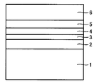
図2を参照して、GaN基板1の上にn型GaNエピタキシャル層2が位置し、その上にn型AlxGa1-xN層3が形成されている。その上にAlxGa1-xN層とAlxInyGa1-x-yN層とからなる量子井戸(MQW:Multi-Quantum Well)4が形成されている。その量子井戸4をn型AlxGa1-xN層3とはさむようにp型AlxGa1-xN層5が配置されている。また、p型AlxGa1-xN層5の上にp型GaN層6が配置されている。上記の構造においては、量子井戸4において発光する。また、図1に示すように、p型GaN層6の上に、p電極12がp型GaN層6の上部表面の全面を被覆するように形成され、ダウン実装される。
Referring to FIG. 2, n-type GaN
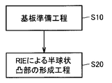
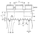
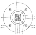
次に、図3〜図5を参照して、図1および図2に示したLEDの製造方法について簡単に説明する。図3は、図1および図2に示したLEDを構成するチップの製造方法を示すフローチャートである。図4は、図2に示した構造のチップをウエハから採取するときのウエハの状態を示す図である。図5は、図4に示した電極の配置を示す図である。 Next, a method for manufacturing the LED shown in FIGS. 1 and 2 will be briefly described with reference to FIGS. FIG. 3 is a flowchart showing a manufacturing method of a chip constituting the LED shown in FIGS. 1 and 2. FIG. 4 is a view showing a state of the wafer when the chip having the structure shown in FIG. 2 is taken from the wafer. FIG. 5 is a diagram showing the arrangement of the electrodes shown in FIG.
まず、図3に示した基板準備工程(S10)を実施する。具体的には、まず、GaN基板を準備する。そして、当該GaN基板の第1の主表面上にMOCVD(Metal Organic Chemical Vapor Deposition)などの成膜方法を用いて積層構造(Siドープn型GaN層/クラッド層のSiドープn型Al0.2Ga0.8N層/GaN層とIn0.15Ga0.85N層との2層構造が複数層重ねられたMQW(Multi-Quantum Well)/クラッド層のMgドープp型Al0.2Ga0.8N層/Mgドープp型GaN層)を形成する。次に、このウエハを活性化処理して、Mgドープp型層の低抵抗化を行なってもよい。このウエハをさらに、フォトリソグラフィ技術とRIE(Reactive Ion Etching)により、Mgドープp型層側からSiドープn型層までCl系ガスでエッチングする。このエッチングにより、図4に示すように、素子分離溝25を形成し、素子分離を行なう。
First, the substrate preparation step (S10) shown in FIG. 3 is performed. Specifically, first, a GaN substrate is prepared. Then, a laminated structure (Si-doped n-type GaN layer / Si-doped n-type Al 0.2 Ga 0.8 of cladding layer) is formed on the first main surface of the GaN substrate using a film forming method such as MOCVD (Metal Organic Chemical Vapor Deposition). MQW (Multi-Quantum Well) / Clad layer Mg-doped p-type Al 0.2 Ga 0.8 N layer / Mg-doped p-type GaN with multiple layers of two-layer structure of N layer / GaN layer and In 0.15 Ga 0.85 N layer Layer). Next, the wafer may be activated to reduce the resistance of the Mg-doped p-type layer. The wafer is further etched with a Cl-based gas from the Mg-doped p-type layer side to the Si-doped n-type layer by photolithography and RIE (Reactive Ion Etching). By this etching, as shown in FIG. 4, an
次に、GaN基板の第2の主面(主表面)である裏面のN面に、フォトリソグラフィ技術と、蒸着と、リフトオフ法とにより所定の間隔(距離L2)でチップの中心に平面形状が四角形状のn電極11を形成する(図4および図5参照)。n電極11としては、GaN基板に接して下から順に(Ti層/Al層/Ti層/Au層)という積層構造を形成してもよい。そして、n電極11とGaN基板の裏面との接触抵抗を所定の値とするため、窒素(N2)雰囲気中でGaN基板を加熱する。
Next, a planar shape is formed at the center of the chip at a predetermined interval (distance L 2 ) on the N-side of the back surface, which is the second main surface (main surface) of the GaN substrate, by photolithography technology, vapor deposition, and lift-off method. Forms a square-shaped n-electrode 11 (see FIGS. 4 and 5). As the
次に、p電極としてはp型GaN層に接して所定の厚みを有する導電体層を形成する。導電体層としては、たとえばGaN層に接するように所定の厚みのNi層を形成し、その上に所定の厚みのAu層を全面に形成してもよい(図4および図5参照)。この場合、p電極とp型GaN層との接触抵抗を所定の値とするため、GaN基板を不活性ガス雰囲気中で加熱処理してもよい。 Next, as a p-electrode, a conductor layer having a predetermined thickness is formed in contact with the p-type GaN layer. As the conductor layer, for example, a Ni layer having a predetermined thickness may be formed so as to be in contact with the GaN layer, and an Au layer having a predetermined thickness may be formed on the entire surface (see FIGS. 4 and 5). In this case, in order to set the contact resistance between the p electrode and the p-type GaN layer to a predetermined value, the GaN substrate may be heat-treated in an inert gas atmosphere.
次に、図3のRIEによる半球状凸部の形成工程(S20)を実施する。具体的には、GaN基板の裏面(N面)に、RIEを施すことにより半球状の凸部82を形成する。RIEで用いる反応ガスとしては、たとえば塩素ガス(Clガス)を用いることができる。このとき、N面におけるn電極11が形成された領域の外周部もRIEにより部分的に除去されるので、結果的にn電極11の下に頂面が平坦な凸部が形成されることになる。この凸部の頂面上にn電極11が配置された状態になる。また、N面におけるn電極11が形成された領域以外の領域では、RIEにより半球状の凸部82が形成される。この凸部82の幅W(図4参照)は凸部82の高さの2倍程度になる。凸部82の高さは0.2μm以上100μm以下である。なお、上述したn電極11の形成工程より先にRIEによる半球状凸部の形成工程(S20)を実施してもよい。
Next, a step of forming a hemispherical protrusion by RIE in FIG. 3 (S20) is performed. Specifically, hemispherical
その後に、図4および図5に示すように、チップ境界50が側面として現れるようにスクライブを行ない、チップ化したものを発光装置とした。そして、図1を参照して、リードフレームのマウント部21aに、上記チップのp型GaN層側が接するように搭載して、発光装置を形成した。マウント部に塗布した導電性接着剤14によって発光装置とマウントとを固定するとともに、導通が得られるようにしている。そして、n電極11とリードフレームのリード部とをワイヤボンドにより導通させた後、エポキシ系樹脂15により樹脂封止を行なって発光装置をランプ化した。なお、発光装置からの放熱性を良くするために、発光装置のp型GaN層が全面マウント部と接するように搭載してもよい。また導電性接着剤14は熱伝導の良いAg系のものを、またリードフレームも熱伝導の良いCuW系のものを選択してもよい。
Thereafter, as shown in FIG. 4 and FIG. 5, scribing was performed so that the
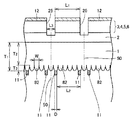
図6は、図1〜図5に示した本発明によるLEDの実施の形態1の変形例を示す図である。図7は、図6に示したLEDの平面形状を示す図である。図6および図7を参照して、本発明によるLEDの実施の形態1の変形例を説明する。
FIG. 6 is a diagram showing a modification of the first embodiment of the LED according to the present invention shown in FIGS. FIG. 7 is a diagram showing a planar shape of the LED shown in FIG. With reference to FIG. 6 and FIG. 7, the modification of
図6および図7に示したLEDは、基本的には図1および図2に示したLEDと同様の構造を備えるが、n電極11をGaN基板の四隅、すなわち4つのコーナー近傍に配置した点が図1及び図2に示したLEDと異なる。また、図6および図7に示したLEDでは、半導体チップの実装において半導体チップを取り囲むようにリードフレームに反射カップ37を配置している。
The LED shown in FIGS. 6 and 7 basically has the same structure as the LED shown in FIGS. 1 and 2, except that the n-
図6および図7に示したLEDの製造方法は、基本的に図1および図2に示したLEDの製造方法と同様である。ここで、図8は、図6および図7に示したLEDを構成する積層構造のチップをウエハから採取するときのウエハの状態を示す図である。この場合、1つのチップあたりのn電極11の数が増えたことに対応して、n電極11のそれぞれの面積を図1および図2に示したLEDのn電極11の面積より小さくすることが好ましい。
The manufacturing method of the LED shown in FIGS. 6 and 7 is basically the same as the manufacturing method of the LED shown in FIGS. 1 and 2. Here, FIG. 8 is a view showing a state of the wafer when the chip having the laminated structure constituting the LED shown in FIGS. 6 and 7 is taken from the wafer. In this case, in response to the increase in the number of
(実施の形態2)
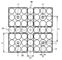
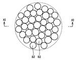
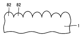
上述した実施の形態1においては、GaN基板1をスクライブによりチップ化したものをリードフレームに搭載して発光装置とした場合を説明した。しかし、発光装置を構成するチップとなるようにGaN基板1を分割することなく、たとえば図9に示すように、GaN基板1において半球状の凸部82を形成したはRIEによる半球状凸部の形成工程(S20)(図3参照)を行なった状態の基板として取り扱う方が、ハンドリングが容易な場合がある。図9は、本発明による発光装置を構成するチップとなるべき領域を複数個含む、本発明によるGaN基板の実施の形態2を示す模式図である。図10は、図9に示した領域Xの拡大平面模式図である。図11は、図10の線分XI−XIにおける断面模式図である。図9〜図11に示すように、GaN基板1の1つの主表面である第2の主表面1aには複数の半球状の凸部82が形成されている。このような複数のチップを、分割する前のGaN基板1として取り扱うことで、当該複数のチップのハンドリングが容易になる。
(Embodiment 2)
In the first embodiment described above, the case where the
本発明による発光装置の効果を確認するべく、以下のような試料を準備して所定の電流を入力した場合の青色光出力の値を測定した。以下、準備した試料についてまず説明する。
(本発明例1):本発明例1のLEDは、基本的に図1および図2に示したLEDと同様の構造を備える。発明例1のLEDの製造方法も、基本的に図3〜図5を参照して説明した発光装置の製造方法と同様である。以下、具体的に説明する。
(S1−1)c面から0.5°ずらしたGaNのオフ基板を使用した。この基板の酸素濃度は5E18/cm3、転位密度は1E7/cm2であり、厚みは400μmとした。
(S1−2)MOCVD(Metal Organic Chemical Vapor Deposition)でGaN基板の第1の主面であるGa面上に次の積層構造を形成した。(Siドープn型GaN層/クラッド層のSiドープn型Al0.2Ga0.8N層/GaN層とIn0.15Ga0.85N層との2層構造が3層重ねられたMQW(Multi-Quantum Well)/クラッド層のMgドープp型Al0.2Ga0.8N層/Mgドープp型GaN層)
(S1−3)発光波長は450nmである。
(S1−4)このウエハを活性化処理して、Mgドープp型層の低抵抗化を行なった。ホール測定によるキャリア濃度は、Mgドープp型Al0.2Ga0.8N層が5E17/cm3、Mgドープp型GaN層が1E18/cm3であった。
(S1−5)このウエハをさらに、フォトリソグラフィ技術とRIE(Reactive Ion Etching)により、Mgドープp型層側からSiドープn型層までCl系ガスでエッチングする。このエッチングにより、図4に示すように、素子分離溝25を形成し、素子分離を行なった。素子分離溝の幅L3は100μmである。
(S1−6)GaN基板の第2の主面である裏面のN面には、フォトリソグラフィ技術と、蒸着と、リフトオフ法とにより、図4に示した距離L2=2mmおきにチップの中心に平面形状が正方形状であり、1辺の幅(D)が200μmの(200μm□の)n電極をつけた(図4および図5参照)。n電極として、GaN基板1に接して下から順に(Ti層20nm/Al層100nm/Ti層20nm/Au層200nm)の積層構造を形成した。これを窒素(N2)雰囲気中で加熱することにより、接触抵抗を1E−5Ω・cm2以下とした。
(S1−7)p電極としてはp型GaN層に接して厚み4nmのNi層を形成し、その上に厚み4nmのAu層を全面に形成した(図4および図5参照)。これを不活性ガス雰囲気中で加熱処理することにより、接触抵抗を5E−4Ω・cm2とした。
(S1−8)その後、基板のN面に対して反応性イオンエッチング(RIE)を行なった。この結果、当該N面の表面層を部分的に除去することによって当該N面において半球状の凸部82を複数個形成した。上に断面形状がV字状の溝80を形成した。図4に示すように、ドーム状の凸部82の高さT3は平均値が30μm、凸部82の幅は60μmとした。なお、反応性イオンエッチングの具体的なプロセス条件は、以下の通りである。まず、RIE装置の処理容器内部にGaN基板1のN面が上を向くように設置した。そして、プロセス条件として、処理容器内部の圧力を20mtorr、印加パワーを300W、反応ガスを100%塩素(Cl2)ガス、反応ガスとしての塩素ガスの流量を50sccm(standard cc/min)(すなわち0.05リットル/分)、処理時間を120分、といった条件を用いて、RIE処理を行なった。この結果、図1、図4および図5に示すように、基板のN面には半球状の凸部82が複数個形成された。
(S1−9)その後に、図4および図5に示すように、チップ境界50が側面として現れるようにスクライブを行ない、チップ化したものを発光装置とした。チップ化した発光装置は、光の放出面が1.9mm□(1辺の長さが1.9mmの四角形)の形状で、発光層が1.9mm□の形状をとる。すなわち図5において、L1=1.9mmであり、L2=2mmである。また、素子分離溝の幅L3=100μmであり、n電極の1つの辺の幅D=200μm(n電極は200μm□)である。
(S1−10)図1を参照して、リードフレームのマウント部21aに、上記チップのp型GaN層側が接するように搭載して、発光装置を形成した。マウント部に塗布した導電性接着剤14によって発光装置とマウントとを固定するとともに、導通が得られるようにしている。
(S1−11)発光装置からの放熱性を良くするために、発光装置のp型GaN層が全面マウント部と接するように搭載した。また接着剤は熱伝導の良いAg系のものを、またリードフレームも熱伝導の良いCuW系のものを選択した。これにより、得られた熱抵抗は8℃/Wであった。
(S1−12)さらに、n電極とリードフレームのリード部とをワイヤボンドにより導通させた後、エポキシ系樹脂により樹脂封止を行なって発光装置をランプ化した。
(比較例1):比較例1のLEDは、基本的に上記本発明例1のLEDと同様の構造を備えるが、GaN基板1のN面に形成された半球状の凸部のサイズが本発明例1のLEDと異なる。すなわち、比較例1のLEDでは、GaN基板1のN面に形成された半球状の凸部の平均的な高さが20nm(0.02μm)であり、当該凸部の幅が40nm(0.04μm)である。
In order to confirm the effect of the light emitting device according to the present invention, the following sample was prepared and the blue light output value was measured when a predetermined current was input. Hereinafter, the prepared sample will be described first.
(Invention Example 1): The LED of Invention Example 1 basically has the same structure as the LED shown in FIGS. The manufacturing method of the LED of Invention Example 1 is basically the same as the manufacturing method of the light emitting device described with reference to FIGS. This will be specifically described below.
(S1-1) A GaN off-substrate shifted by 0.5 ° from the c-plane was used. This substrate had an oxygen concentration of 5E18 / cm 3 , a dislocation density of 1E7 / cm 2 , and a thickness of 400 μm.
(S1-2) The following laminated structure was formed on the Ga surface, which is the first main surface of the GaN substrate, by MOCVD (Metal Organic Chemical Vapor Deposition). (SiW-doped n-type GaN layer / Clad layer Si-doped n-type Al 0.2 Ga 0.8 N layer / MQW (Multi-Quantum Well) / two layers of GaN layer and In 0.15 Ga 0.85 N layer) (Clad layer Mg-doped p-type Al 0.2 Ga 0.8 N layer / Mg-doped p-type GaN layer)
(S1-3) The emission wavelength is 450 nm.
(S1-4) This wafer was activated to reduce the resistance of the Mg-doped p-type layer. The carrier concentration by hole measurement was 5E17 / cm 3 for the Mg-doped p-type Al 0.2 Ga 0.8 N layer and 1E18 / cm 3 for the Mg-doped p-type GaN layer.
(S1-5) The wafer is further etched with a Cl-based gas from the Mg-doped p-type layer side to the Si-doped n-type layer by photolithography and RIE (Reactive Ion Etching). By this etching, as shown in FIG. 4, an
(S1-6) The N-side of the back surface, which is the second main surface of the GaN substrate, is centered on the chip at intervals of L2 = 2 mm shown in FIG. 4 by photolithography, vapor deposition, and lift-off method. An n-electrode having a square shape in plan and having a side width (D) of 200 μm (200 μm square) was attached (see FIGS. 4 and 5). As the n-electrode, a stacked structure of (
(S1-7) As a p-electrode, a 4 nm thick Ni layer was formed in contact with the p-type GaN layer, and a 4 nm thick Au layer was formed on the entire surface (see FIGS. 4 and 5). This was heat-treated in an inert gas atmosphere, so that the contact resistance was 5E-4 Ω · cm 2 .
(S1-8) Thereafter, reactive ion etching (RIE) was performed on the N surface of the substrate. As a result, a plurality of hemispherical
(S1-9) Thereafter, as shown in FIGS. 4 and 5, scribing was performed so that the
(S1-10) Referring to FIG. 1, the chip was mounted so that the p-type GaN layer side of the chip was in contact with the
(S1-11) In order to improve the heat dissipation from the light emitting device, the p-type GaN layer of the light emitting device was mounted so as to be in contact with the entire mount portion. Also, an Ag-based adhesive with good thermal conductivity was selected, and a lead frame of CuW-based adhesive with high thermal conductivity was selected. Thereby, the obtained thermal resistance was 8 ° C./W.
(S1-12) Further, the n electrode and the lead portion of the lead frame were made conductive by wire bonding, and then resin sealing was performed with an epoxy resin to form a lamp.
(Comparative Example 1): The LED of Comparative Example 1 basically has the same structure as the LED of Example 1 of the present invention, but the size of the hemispherical convex portion formed on the N face of the
比較例1のLEDの製造方法は、以下のようなものである。
(S2−1)〜(S2−7):基本的に本発明例1の(S1−1)〜(S1−7)と同様である。
(S2−8):基本的に本発明例1の(S1−8)と同様であるが、RIEのプロセス条件が異なる。具体的には、RIEの処理時間を5秒としている。この結果、形成される半球状の凸部82の平均的な高さは20nm(0.02μm)、凸部82の幅は40nm(0.04μm)となった。
(S2−9)〜(S2−12):基本的に本発明例1の(S1−9)〜(S1−12)と同様である。つまり、比較例1のLEDの製造方法は、本発明例1の製造方法と基本的に同様であるが、本発明例1の工程(S1−8)に対応する工程(S2−8)におけるRIEの処理時間が異なる(比較例1ではRIEの処理時間が短くなっている)。このため、形成される凸部82の高さや幅が本発明例1の当該高さや幅より小さくなっている。
(比較例2):比較例2のLEDは、基本的に上記比較例1のLEDと同様の構造を備えるが、図12に示すようにGaN基板1のN面に半球状の凸部が形成されていない点が異なる。図12は、比較例2のLEDを示す模式図である。
The manufacturing method of the LED of Comparative Example 1 is as follows.
(S2-1) to (S2-7): Basically the same as (S1-1) to (S1-7) of Example 1 of the present invention.
(S2-8): Basically the same as (S1-8) of Example 1 of the present invention, but the RIE process conditions are different. Specifically, the RIE processing time is 5 seconds. As a result, the average height of the formed hemispherical
(S2-9) to (S2-12): Basically the same as (S1-9) to (S1-12) of Example 1 of the present invention. That is, the manufacturing method of the LED of Comparative Example 1 is basically the same as the manufacturing method of Example 1 of the present invention, but the RIE in the step (S2-8) corresponding to the step (S1-8) of Example 1 of the present invention. (The comparative example 1 has a shorter RIE processing time). For this reason, the height and width of the
(Comparative Example 2): The LED of Comparative Example 2 basically has the same structure as the LED of Comparative Example 1, but a hemispherical protrusion is formed on the N surface of the
比較例2のLEDの製造方法は、以下の通りである。
(S3−1)〜(S3−7):基本的に本発明例1の(S1−1)〜(S1−7)と同様である。
(S3−8)〜(S3−11):基本的に本発明例1の(S1−9)〜(S1−12)と同様である。
The manufacturing method of the LED of Comparative Example 2 is as follows.
(S3-1) to (S3-7): Basically the same as (S1-1) to (S1-7) of Example 1 of the present invention.
(S3-8) to (S3-11): Basically the same as (S1-9) to (S1-12) of Example 1 of the present invention.
(試験およびその結果)
本発明例1および比較例1、2を、それぞれ積分球内に搭載した後所定の電流(2A)を印加して、集光されディテクタから出力される光出力値の比較を行なった。その結果、本発明例1は1.1Wの出力が得られた。一方、比較例1の出力は0.8W、比較例2の出力は0.8Wであった。このように、GaN基板の光出射面側(第2の主面側)をRIEにより加工することで所定の大きさの半球状の凸部82を形成した本発明例1は、GaN基板1とエポキシ樹脂15との接触界面の面積が比較的大きいこと、当該界面が発光層の面に対して様々な角度を有することから界面での全反射が防止されやすいこと、などの理由により、比較例1、2より本発明例1は高い光出力を得ることができる。
(Test and results)
Inventive Example 1 and Comparative Examples 1 and 2 were each mounted in an integrating sphere, and then a predetermined current (2A) was applied to compare the light output values collected and output from the detector. As a result, Example 1 of the present invention obtained an output of 1.1 W. On the other hand, the output of Comparative Example 1 was 0.8 W, and the output of Comparative Example 2 was 0.8 W. Thus, the present invention example 1 in which the hemispherical
なお、上述した本発明例1と比較例1とは、半球状の凸部82のサイズのみが異なるが、そのような半球状凸部82のサイズ(高さ)と得られる光出力との関係をシミュレーションにより求めた。その結果を図13に示す。図13は、半球状凸部の高さと光出力との関係をシミュレーションにより求めた結果を示すグラフである。図13の横軸は半球状凸部の高さ(単位:μm)を示している。横軸は対数目盛で示されている。また、図13の縦軸は得られる光出力(単位:W)を示している。図13では、上述した本発明例1および比較例1の実験結果が黒塗り四角で示され、シミュレーションにより求めた半球状凸部の高さと光出力との関係が実線で示されている。図13から分かるように、半球状凸部82の高さが1μmを超えると、LEDからの光出力が急激に向上する。
The above-described inventive example 1 and comparative example 1 differ only in the size of the hemispherical
なお、シミュレーションの前提としては、LEDの基本的な構成は本発明例1と同様として、密集して形成された半球状凸部(ドーム構造)が全て半球状であると仮定した。また、半球状凸部の高さは、当該凸部の高さの平均的な高さとした。ここで、平均的な高さ(および幅)とは、たとえば所定個数の凸部についてその高さ(および幅)を測定し、平均値を算出することにより決定する。具体的には、基板のN面での任意の3箇所について、所定の倍率で観察した視野内において任意に選択した5つの凸部に関して、高さおよび幅を測定する。そして、こられ3箇所×5つの凸部=15個の凸部について高さおよび幅のデータを測定し、これらの高さおよび幅のそれぞれのデータについて平均値を算出する。このようにして、凸部の平均的な高さおよび幅を得ることができる。 As a premise of the simulation, the basic configuration of the LED is the same as that of Example 1 of the present invention, and it is assumed that the densely formed hemispherical convex portions (dome structure) are all hemispherical. In addition, the height of the hemispherical convex portion is an average height of the convex portion. Here, the average height (and width) is determined, for example, by measuring the height (and width) of a predetermined number of convex portions and calculating the average value. Specifically, the height and width are measured for five convex portions arbitrarily selected in a field of view observed at a predetermined magnification at arbitrary three locations on the N-plane of the substrate. Then, height and width data are measured for these three locations × 5 convex portions = 15 convex portions, and an average value is calculated for each of these height and width data. In this way, the average height and width of the convex portion can be obtained.
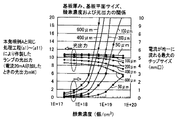
本発明の実施例2では、GaN基板の酸素濃度と比抵抗および光の透過率との関係を把握した。その関係に基づいてpダウン実装、すなわちGaN基板を光放出面とする発光素子において、所定の光放出面積の場合に最適なGaN基板厚みと酸素濃度との関係を樹立した点に特徴がある。上述のようにpダウン実装では光放出面がGaN基板となるので、つぎに示すように、比抵抗と光透過率とに大きな影響を有する酸素濃度はとくに重要である。 In Example 2 of the present invention, the relationship between the oxygen concentration of the GaN substrate, the specific resistance, and the light transmittance was determined. Based on this relationship, p-down mounting, that is, in a light emitting device having a GaN substrate as a light emission surface, is characterized in that an optimum relationship between the GaN substrate thickness and the oxygen concentration is established for a predetermined light emission area. As described above, since the light emission surface is a GaN substrate in the p-down mounting, the oxygen concentration having a large influence on the specific resistance and the light transmittance is particularly important as described below.
図14は、GaN基板の比抵抗に及ぼす酸素濃度の影響を示す図である。図14より、比抵抗0.5Ωcm以下は、酸素濃度1E17個/cm3以上とすることにより実現することができる。また、図15は、GaN基板の厚みが400μmのときの波長450nmの光の透過率に及ぼす酸素濃度の影響を示す図である。同図より酸素濃度が2E19個/cm3を超えると波長450nmの光の透過率が急激に低下することが分かる。図14と図15とから、酸素濃度の増大は、GaN基板の比抵抗を減少させ、発光面を拡大するのに有効であるが光の透過率を低下させることが分かる。したがって、pダウン実装される発光素子に用いられるGaN基板としては酸素濃度、GaN基板の厚さ、発光の平面サイズをどのように設定するかが非常に重要となる。 FIG. 14 is a diagram showing the influence of the oxygen concentration on the specific resistance of the GaN substrate. From FIG. 14, the specific resistance of 0.5 Ωcm or less can be realized by setting the oxygen concentration to 1E17 / cm 3 or more. FIG. 15 is a diagram showing the influence of the oxygen concentration on the transmittance of light having a wavelength of 450 nm when the thickness of the GaN substrate is 400 μm. From the figure, it can be seen that when the oxygen concentration exceeds 2E19 atoms / cm 3 , the transmittance of light having a wavelength of 450 nm rapidly decreases. 14 and 15, it can be seen that increasing the oxygen concentration reduces the specific resistance of the GaN substrate and is effective for enlarging the light emitting surface, but lowers the light transmittance. Therefore, how to set the oxygen concentration, the thickness of the GaN substrate, and the planar size of light emission is very important for a GaN substrate used for a light-emitting element mounted in a p-down manner.
図16は図1に示した本発明によるLEDに対して厚みおよび酸素濃度を変化させたGaN基板からランプを作製したとき、そのランプの光出力および電流が均一に流れる平面サイズを測定した結果を示す図である。なお、検討したLEDは、基本的に上述した本発明例1と同様の処理工程により作成した。 FIG. 16 shows the result of measuring the plane size through which the light output and current of the lamp flow uniformly when a lamp is fabricated from a GaN substrate with the thickness and oxygen concentration varied with respect to the LED according to the present invention shown in FIG. FIG. The studied LEDs were basically produced by the same processing steps as those of the first invention example described above.
図16から分かるように、ランプの光出力についていえば、厚みが厚いほど、また酸素濃度が高いほど光出力は低下する傾向にある。また電流が均一に流れる最大の平面サイズについていえば、厚みが厚いほど、また酸素濃度が高いほど大きくなる傾向にある。 As can be seen from FIG. 16, regarding the light output of the lamp, the light output tends to decrease as the thickness increases and the oxygen concentration increases. As for the maximum planar size through which current flows uniformly, the thickness tends to increase as the thickness increases and the oxygen concentration increases.
図16から、たとえば電流が均一に流れる平面サイズが一辺4mm(一辺5mm)の正方形とする場合、光出力として、光の放出面が300μm□(1辺の長さが300μmの四角形)の形状で、発光層が300μm□の形状をとる本発明によるLEDで20mA印加時に8mW相当以上を得たいとき、厚み200μmのGaN基板では酸素濃度を6E18個/cm3以上(一辺5mm正方形では8E18個/cm3以上)とすれば、上記本発明によるLEDの大きさで20mA印加時に光出力8mW以上を確保した上で、均一な発光を得ることができる。つまり上記本発明によるLEDの大きさ一辺300μmの正方形における20mA印加と電流密度を合わせた場合、一辺4mm(一辺5mm)の正方形では3.6A(5.6A)印加に相当し、3.6A(5.6A)印加時に印加電流に比例して光出力1.4W(2.3W)以上確保した上で、均一な発光を得ることができる。 From FIG. 16, for example, when the plane size in which current flows uniformly is a square with a side of 4 mm (side of 5 mm), the light output surface has a shape of 300 μm □ (a square with a side length of 300 μm). When the LED according to the present invention in which the light emitting layer has a shape of 300 μm □ is desired to obtain 8 mW or more when 20 mA is applied, the oxygen concentration is 6E18 / cm 3 or more for a GaN substrate having a thickness of 200 μm (8E18 / cm3 for a 5 mm square). 3 or more), it is possible to obtain uniform light emission while securing a light output of 8 mW or more when 20 mA is applied with the size of the LED according to the present invention. That is, when the current density is combined with the 20 mA application in the square of 300 μm side of the LED according to the present invention, the square of 4 mm (5 mm side) corresponds to 3.6 A (5.6 A) application, and 3.6 A (3.6 A ( 5.6 A) Uniform light emission can be obtained after securing an optical output of 1.4 W (2.3 W) or more in proportion to the applied current during application.
また、厚み400μmのGaN基板では、上記厚み200μmの場合と同じ目標性能としたとき、一辺4mm正方形では3E18個/cm3以上(一辺5mm正方形の場合、酸素濃度4E18個/cm3以上)とすればよい。ただし、厚み400μmでは酸素濃度を2E19個/cm3以下にしないと上記本発明によるLEDの大きさで20mA印加時に8mW相当以上の光出力を得ることができない。 By addition, the GaN substrate having a thickness of 400 [mu] m, when the same target performance as that of the thickness 200 [mu] m, and 3E18 atoms / cm 3 or more in one side 4mm square (in the case of side 5mm square, oxygen concentration 4E18 / cm 3 or higher) That's fine. However, if the oxygen concentration is not less than 2E19 / cm 3 at a thickness of 400 μm, a light output equivalent to 8 mW or more cannot be obtained when 20 mA is applied with the size of the LED according to the present invention.
さらに、厚み600μmのGaN基板では、一辺4mm正方形の領域を電流が均一に流れる酸素濃度2.5E18個/cm3以上に比して、上述した本発明によるLEDの大きさで20mA印加時に光出力8mW相当以上となる酸素濃度の限界値は2.5E18個/cm3よりわずかに高いだけである。したがって、上記2つの条件を満たす酸素濃度範囲は狭い範囲しかない。一方、一辺3mm正方形の領域に均一に電流が流れる酸素濃度2E18個/cm3程度以上なので、一辺4mm正方形に比較して酸素濃度の許容範囲はわずかに広くなる。 Further, in the case of a GaN substrate having a thickness of 600 μm, compared to an oxygen concentration of 2.5E18 / cm 3 or more in which a current flows uniformly in a square area of 4 mm on one side, the light output is applied when 20 mA is applied in the size of the LED according to the present invention described above. The limit value of the oxygen concentration corresponding to 8 mW or more is only slightly higher than 2.5E18 / cm 3 . Therefore, the oxygen concentration range that satisfies the above two conditions is only a narrow range. On the other hand, since the oxygen concentration is more than about 2E18 / cm 3 in which current flows uniformly in a 3 mm square area, the allowable range of oxygen concentration is slightly wider than that of a 4 mm square.
また、図16によれば、GaN基板の厚みが200μm〜400μmの場合、一辺10mmの正方形に均一に電流を流し、上記本発明によるLEDの大きさで20mA印加時に8mW相当以上の出力を得ることを可能にする酸素濃度範囲は実用上十分広いことが分かる。厚み200μmでは酸素濃度2E19個/cm3より低い酸素濃度以上で可能であることが分かる。また厚み400μmでは酸素濃度8E18/cm3以上で可能である。 In addition, according to FIG. 16, when the thickness of the GaN substrate is 200 μm to 400 μm, a current is uniformly applied to a square with a side of 10 mm, and an output equivalent to 8 mW or more is obtained when 20 mA is applied with the size of the LED according to the present invention. It can be seen that the oxygen concentration range enabling the above is sufficiently wide for practical use. It can be seen that a thickness of 200 μm is possible at an oxygen concentration lower than an oxygen concentration of 2E19 / cm 3 . Further, when the thickness is 400 μm, an oxygen concentration of 8E18 / cm 3 or more is possible.
次に、上記の実施例と重複するものもあるが本発明の実施例を羅列的に挙げて説明する。 Next, although there are some overlapping with the above embodiments, embodiments of the present invention will be listed and described.
この発明に従った発光装置は、図1や図6に示すように、窒化物半導体基板(GaN基板1)と、窒化物半導体基板の第1の主表面の側に、n型窒化物半導体層(n型AlxGa1-xN層3)と、窒化物半導体基板から見てn型窒化物半導体層より遠くに位置するp型窒化物半導体層(p型AlxGa1-xN層5)と、n型窒化物半導体層およびp型窒化物半導体層の間に位置する発光層(量子井戸(MQW:Multi-Quantum Well)4)とを備えた発光装置である。当該発光装置では、p型窒化物半導体層の側をダウン実装し、窒化物半導体基板の第1の主表面と反対側の主表面である第2の主表面1aから光を放出する。窒化物半導体基板の第2の主表面1aには半球状の凸部82が形成されている。
As shown in FIGS. 1 and 6, the light emitting device according to the present invention includes a nitride semiconductor substrate (GaN substrate 1) and an n-type nitride semiconductor layer on the first main surface side of the nitride semiconductor substrate. (N-type Al x Ga 1-x N layer 3) and a p-type nitride semiconductor layer (p-type Al x Ga 1-x N layer located far from the n-type nitride semiconductor layer when viewed from the nitride semiconductor substrate) 5) and a light emitting device (MQW: Multi-Quantum Well (MQW) 4) located between the n-type nitride semiconductor layer and the p-type nitride semiconductor layer. In the light emitting device, the p-type nitride semiconductor layer side is down-mounted, and light is emitted from the second
このようにすれば、窒化物半導体基板の光の出射面である第2の主表面1aに半球状の凸部82を形成するので、当該凸部82がレンズ効果を奏することにより第2の主表面1aに垂直な方向に向かう光を効率的に取出すことができる。この結果、凸部82が形成されていない場合や、単純に第2の主表面1aをKOH溶液などを用いて非鏡面化した場合、さらには第2の主表面1aにダイシングなどを用いて溝を形成した場合より、発光装置における光の利用効率を向上させることができる。
In this case, since the hemispherical
また、上述した構成では、電気抵抗の低い窒化物半導体基板(GaN基板1)の裏面(第2の主表面)にn型電極11を設けるので、小さな被覆率すなわち大きな開口率でn電極11を設けても電流を窒化物半導体基板全体にゆきわたらせて流すことができる。このため、放出面で光を吸収される率が小さくなり、発光効率を高くすることができる。なお、光の放出は第2の主表面だけでなく側面からなされてもよいことは言うまでもない。以下の発光装置においても同様である。
In the above-described configuration, since the n-
また、電気抵抗が高いp型窒化物半導体層の側は光放出面にならないので、p型窒化物半導体層の全面にp型電極層(p電極12)を形成することができ、大電流を流し発熱を抑える上でも、また発生した熱を伝導で逃がす上でも好都合の構造をとることが可能となる。すなわち、熱的要件のために受ける制約が非常に緩和される。このため、電気抵抗を低下させるために、p電極とn電極とを入り組ませた櫛型形状などにする必要がない。 In addition, since the p-type nitride semiconductor layer side having high electrical resistance does not become a light emitting surface, a p-type electrode layer (p-electrode 12) can be formed on the entire surface of the p-type nitride semiconductor layer, and a large current is generated. It is possible to take a convenient structure not only for suppressing flow heat generation but also for releasing generated heat by conduction. That is, the constraints imposed by thermal requirements are greatly relaxed. For this reason, in order to reduce electrical resistance, it is not necessary to make it the comb-shaped shape etc. which interposed the p electrode and the n electrode.
さらに、GaN基板1が導電性に優れることから、サージ電圧に対する保護回路をとくに設ける必要がなく、また耐圧性も非常に優れたものにできる。また、複雑な加工工程を行なうことがないので、製造コストを低減することも容易化される。
Furthermore, since the
なお、上記発光装置において窒化物半導体基板は、GaNまたはAlxGa1-xN(0<x≦1)のいずれかにより構成されていてもよい。この場合、窒化物半導体基板としてGaN基板1を用いれば、基板に印加する電流密度を高くすることができる(大電流密度を印加できる)ため、発光装置において高輝度(および大きな光束)の光を出射できる。また、GaNまたはAlxGa1-xN(0≦x≦1)により窒化物半導体基板を構成すれば、熱伝導のよい、つまり放熱性に優れた窒化物半導体基板を用いて発光装置としてのLEDを構成できる。このため、大電流密度を印加しても、十分放熱を行なうことができるので、熱によりLEDが損傷する可能性を低減できる。したがって、長時間にわたって安定した光を出力できる発光装置を実現できる。
In the above light emitting device, the nitride semiconductor substrate may be composed of either GaN or Al x Ga 1-x N (0 <x ≦ 1). In this case, if the
上記発光装置において、窒化物半導体基板はGaN基板1であってもよい。当該GaN基板1は酸素ドープによりn型化されており、酸素濃度が、酸素原子1E17(1×10¹⁷)個/cm3以上2E19(2×1019)個/cm3以下の範囲にあってもよい。この場合、GaN基板1の全体に均一に電流を流すことができるので、発光装置においてGaN基板1の第2の主表面のほぼ全体から十分な光を出射することができる。
In the light emitting device, the nitride semiconductor substrate may be the
上記発光装置において、半球状の凸部82の高さT3(図4参照)は0.2μm以上100μm以下であってもよく、窒化物半導体基板(GaN基板1)の厚み方向において、凸部82が形成されていない部分の厚みT2(図4参照)は100μm以上600μm以下であってもよい。また、凸部82の幅W(図4参照)は当該凸部82の高さT3の2倍程度、具体的には0.4μm以上200μm以下であってもよい。また、上記凸部82の高さT2や幅Wはそれぞれ凸部82の平均の高さや平均の幅であってもよい。平均の高さおよび幅とは、たとえば所定個数の凸部についてその高さおよび幅を測定し、平均値を算出することにより決定してもよい。具体的には、基板のN面での任意の3箇所について、所定の倍率で観察した視野内において任意に選択した5つの凸部に関して、高さおよび幅を測定する。そして、こられ3箇所×5つの凸部=15個の凸部について高さおよび幅のデータを測定し、これらの高さおよび幅のそれぞれのデータについて平均値を算出することにより、上記平均の高さおよび幅を決定してもよい。
In the light emitting device, the height T3 (see FIG. 4) of the hemispherical
ここで、一般的に光のフレネル反射において、窒化物半導体基板(GaN基板1)での構造の効果が現れて光の取出し効率が向上するのは(取出す光の波長:λ)/(窒化物半導体基板の屈折率:n)程度以上のサイズの構造からである。そして、発光装置から取出す光の波長を420nm〜480nmと考え、窒化物半導体基板がGaN基板1である場合を考えると、当該GaN基板1の屈折率は2.5である。これらのデータに基づいて光の取出し効率が向上する構造のサイズの下限を考える。その結果、当該構造のサイズが0.2μm(200nm)以上であれば、構造の効果が現れて、光の取出し面である第2の主表面1aからの光の取出し効率が向上すると考えられる。また、当該構造のサイズは大きければ大きいほど光の取出し効率の向上には寄与するが、あまり当該構造(凸部82)のサイズ(たとえば高さT3)が大きすぎると、当該凸部82の形成に時間がかかることになる。このように凸部82の形成に時間がかかると、発光装置の製造工期が長くなるので、結果的に発光装置の製造コストを増大させることになる。このため、現実的な処理時間で形成可能な凸部82のサイズ(高さ)としては100μm程度といった数値が考えられる。また、凸部82の幅Wは高さの2倍程度になるので、上記のように当該幅Wは0.4μm以上200μm以下となる。
Here, in general, in the Fresnel reflection of light, the effect of the structure on the nitride semiconductor substrate (GaN substrate 1) appears and the light extraction efficiency is improved (wavelength of extracted light: λ) / (nitride) This is because the semiconductor substrate has a refractive index of about n) or more. Considering the case where the wavelength of light extracted from the light emitting device is 420 nm to 480 nm and the nitride semiconductor substrate is the
また、凸部82が形成されていない部分での窒化物半導体基板の厚み(隣り合う凸部82の間においてGaN基板1の厚みがもっとも薄くなっている部分での厚みT2)については、発光層(MQW4)に供給される電流を広げるために必要な厚みを確保する必要がある。(つまり、GaN基板1の厚みT1(図4参照)が薄すぎると、第2の主表面1a側に設置されたn電極11から供給された電流が発光層の全面に行きわたるように十分に広がらず、発光層の全面から効率的に光を出射させることができなくなる。)したがって、GaN基板に供給された電流を十分に広げるためには、凸部82が形成されていない部分での窒化物半導体基板の厚みT2を100μm以上とすることが好ましい。
Further, regarding the thickness of the nitride semiconductor substrate in the portion where the
一方、できるだけサイズの大きな凸部82を形成するという観点からすると、当該GaN基板1の厚みT1は厚ければ厚いほどよいことになる。しかし、GaN基板1の厚みT1が厚すぎると、GaN基板1を透過して第2の面1aから出射する光の当該GaN基板1における透過量が小さくなる。また、GaN基板1が厚くなるとGaN基板1の材料コストも上昇するので、結果的に発光装置の製造コストを増大させることになる。このような観点からすると、凸部82が形成されていない部分でのGaN基板1の厚みT2の上限を600μm程度とすれば、上記のような光の透過量の問題や製造コストの問題の程度を許容範囲内に収めることができる。
On the other hand, from the viewpoint of forming the
上記発光装置において、半球状の凸部82の高さT3の範囲の下限については、1μm以上、さらに好ましくは2μm以上であることが好ましい。また、上記凸部82の高さT3の範囲の上限については、より好ましくは80μm以下である。
In the light emitting device, the lower limit of the range of the height T3 of the hemispherical
ここで、発明者は発光装置から取出す光が青色光である場合、凸部82の高さを1μm以上とすれば光の取出し効率が飛躍的に向上することを見出した。このため、凸部82の高さの下限を1μmとすることが好ましい。また、当該凸部82の高さを2μm以上とすれば、確実に光の取出し効率の向上効果を得ることができる。
Here, the inventor has found that when the light extracted from the light emitting device is blue light, the light extraction efficiency is dramatically improved if the height of the
上記発光装置において、凸部82は第2の主表面1aに対して反応性イオンエッチングを行なうことにより形成されていてもよい。この場合、ダイシングや研磨加工などを行うことなく、反応性イオンエッチングの実施によって上記凸部82を形成できる。このため、ダイシングなどを行う場合より発光装置の製造工程を簡略化できる。この結果、発光装置の製造コストを低減できる。
In the light emitting device, the
この発明に従った窒化物半導体基板を備える発光装置の製造方法は、窒化物半導体基板を準備する工程(基板を準備する工程(S10))と、半球状の凸部を形成する工程(RIEによる半球状凸部の形成工程(S20))とを備える。半球状の凸部を形成する工程(S20)は、窒化物半導体基板(GaN基板1)において発光層が形成される側である第1の主表面と反対側の第2の主表面1aに、反応性イオンエッチングを行なうことにより、第2の主表面1aの一部を除去することによって半球状の凸部82を形成する。
The method of manufacturing a light emitting device including a nitride semiconductor substrate according to the present invention includes a step of preparing a nitride semiconductor substrate (step of preparing a substrate (S10)) and a step of forming a hemispherical protrusion (by RIE). A step of forming a hemispherical protrusion (S20). The step (S20) of forming the hemispherical convex portion is performed on the second
このようにすれば、ダイシングや研磨加工などを行うことなく、反応性イオンエッチングによって上記凸部82を形成できる。このため、ダイシングなどを行う場合より発光装置の製造工程を簡略化できる。この結果、本発明による発光装置を低コストで製造できる。
In this way, the
この発明に従った窒化物半導体基板(GaN基板1)は、1つの主表面(第2の主表面1a)に半球状の凸部82が形成されている。この場合、当該窒化物半導体基板(GaN基板1)を発光装置の製造に用いて、当該凸部82が形成された面を発光装置の光の取出し面とすれば、凸部82が形成されていない基板を用いる場合より、光の取出し効率の高い発光装置を製造できる。
The nitride semiconductor substrate (GaN substrate 1) according to the present invention has a hemispherical
上記窒化物半導体基板はGaN基板1であってもよい。当該GaN基板1は酸素ドープによりn型化されており、酸素濃度が、酸素原子1E17個/cm3以上2E19個/cm3以下の範囲にあることが好ましい。この場合、GaN基板1の全体に均一に電流を流すことができるので、当該GaN基板1を用いて製造された発光装置において、GaN基板1の第2の主表面のほぼ全体から十分な光を出射することができる。
The nitride semiconductor substrate may be a
なお、窒化物半導体基板としてのGaN基板1における酸素濃度については、酸素濃度が2E19個/cm3を超える場合、GaN基板1の光(特に青色光)に対する透過率が小さくなるので、結果的にGaN基板1での光の透過量が小さくなってしまう。また、GaN基板1における酸素濃度が1E17個/cm3未満の場合、GaN基板1の比抵抗が小さくなるので、電極からGaN基板1に供給された電流が十分広がった状態で発光層4に供給されない。このため、発光装置からの光出力が小さくなる。
As for the oxygen concentration in the
上記窒化物半導体基板において、半球状の凸部82の高さは0.2μm以上100μm以下であってもよい。窒化物半導体基板の厚み方向において、凸部82が形成されていない部分の厚みT2(図4参照)は100μm以上600μm以下であってもよい。また、凸部82の幅W(図4参照)は当該凸部82の高さT3(図4参照)の2倍程度、具体的には0.4μm以上200μm以下であってもよい。
In the nitride semiconductor substrate, the height of the
この場合、凸部82の構造の効果が現れて当該凸部82が形成された面を光の取出し面とした発光装置における光の取出し効率を向上させることができる。なお、凸部82の高さを上述のように0.2μm以上とすれば凸部82の構造の効果を発揮させることができる。また、凸部82の高さT3を100μm以下とすれば、凸部82を形成するための反応性イオンエッチングの処理時間を現実的な処理時間とすることができる。
In this case, the effect of the structure of the
また、凸部82が形成されていない部分での窒化物半導体基板の厚みT2を100μm以上とすれば、当該窒化物半導体基板を用いて発光装置を作成した場合に、発光装置の発光層(MQW4)全体に行きわたるように、当該基板を介して電流を供給することができる。また、凸部82が形成されていない部分での当該基板の厚みT2を600μm以下とすれば、当該基板における光の透過量が低下するといった問題の発生を抑制できる。
Further, when the thickness T2 of the nitride semiconductor substrate in the portion where the
上記窒化物半導体基板において、半球状の凸部82の高さT3の範囲の下限について、1μm以上、さらに好ましくは2μm以上であることが好ましい。また、上記凸部82の高さT3の範囲の上限について、より好ましくは80μm以下である。
In the nitride semiconductor substrate, the lower limit of the range of the height T3 of the hemispherical
このように、凸部82の高さT3を1μm以上とすれば、当該GaN基板1を用いて発光装置を製造したときに、凸部82が形成された面(第2の主表面1a)からの光の取出し効率を、凸部82が形成されていない場合に比べて飛躍的に向上させることができる。また、凸部82の高さT3を2μm以上とすれば、上記光の取出し効率の向上効果を確実に得ることができる。
Thus, if the height T3 of the
上記窒化物半導体基板において、凸部82は第2の主表面1aに対して反応性イオンエッチングを行なうことにより形成されていてもよい。この場合、ダイシングや研磨加工などを行なうことなく、反応性イオンエッチングの実施によって上記凸部82を形成できる。このため、ダイシングなどを行なう場合より窒化物半導体基板の製造工程を簡略化できる。
In the nitride semiconductor substrate, the
上記において、本発明の実施の形態および実施例について説明を行ったが、上記に開示された本発明の実施の形態および実施例は、あくまで例示であって、本発明の範囲はこれら発明の実施の形態に限定されない。本発明の範囲は、特許請求の範囲の記載によって示され、さらに特許請求の範囲の記載と均等の意味および範囲内でのすべての変更を含むものである。 Although the embodiments and examples of the present invention have been described above, the embodiments and examples of the present invention disclosed above are merely examples, and the scope of the present invention is the implementation of these inventions. It is not limited to the form. The scope of the present invention is indicated by the description of the scope of claims, and further includes meanings equivalent to the description of the scope of claims and all modifications within the scope.
本発明の発光装置は、導電性の高い窒化物半導体基板を用い、光の出射面に半球状の凸部を形成し、pダウン実装した構造を用いた結果、(1)光の取出し効率を向上させることができ、(2)放熱性に優れ、複雑な電極構造を設ける必要がなく、大出力の発光を可能にし、(3)導電性に優れ、過渡電圧や静電放電から発光素子を保護するための保護回路を設ける必要がなく、大面積発光および静電耐圧に優れ、(4)発光層から基板にかけて屈折率の大から小への大きな不連続性がないため、発光層から放出面にいたる間で全反射が生じ難く、したがって全反射に起因する、効率低下や側面部の樹脂劣化がなく、(5)低電圧で発光するので、大容量の電源を必要とせず、とくに自動車用の照明装置用に適しており、(6)その構造が簡単なために、製造しやすく安価であり、メインテナンス性にも優れている。このため、今後、自動車の照明装置を含めて各種の照明製品に広範に利用されることが期待される。 The light-emitting device of the present invention uses a highly conductive nitride semiconductor substrate, a hemispherical convex portion is formed on the light exit surface, and a p-down mounting structure is used. As a result, (1) light extraction efficiency is improved. (2) Excellent heat dissipation, no need to provide a complicated electrode structure, enabling high-output light emission, (3) Excellent conductivity, light emitting element from transient voltage and electrostatic discharge There is no need to provide a protective circuit for protection, and it excels in large-area light emission and electrostatic withstand voltage. Total reflection is unlikely to occur between the surfaces, and therefore there is no reduction in efficiency or resin degradation due to total reflection, and (5) light is emitted at a low voltage, so a large-capacity power supply is not required. (6) Simple structure. For such a low cost easy to manufacture, it is excellent in maintainability. For this reason, it is expected that it will be widely used in various lighting products including automotive lighting devices in the future.
1 GaN基板、1a 光放出面(第2の主表面)、2 n型GaN層、3 n型AlxGa1-xN層、4 MQW(発光層)、5 p型AlxGa1-xN層、6 p型GaN層、11 n電極、12 p電極、13 ワイヤ、14 導電性接着剤、15 エポキシ系樹脂、21a リードフレームのマウント部、21b リードフレームのリード部、25 素子分離溝、50 チップ境界、82 半球状の凸部。 1 GaN substrate, 1a light emission surface (second main surface), 2 n-type GaN layer, 3 n-type Al x Ga 1-x N layer, 4 MQW (light emitting layer), 5 p-type Al x Ga 1-x N layer, 6 p-type GaN layer, 11 n electrode, 12 p electrode, 13 wire, 14 conductive adhesive, 15 epoxy resin, 21a lead frame mount, 21b lead frame lead, 25 element isolation groove, 50 Chip boundary, 82 Hemispherical convex part.
Claims (6)
前記p型窒化物半導体層の側をダウン実装し、前記窒化物半導体基板の前記第1の主表面と反対側の主表面である第2の主表面から光を放出し、
前記窒化物半導体基板の前記第2の主表面には半球状の凸部が形成されている、発光装置。 A nitride semiconductor substrate, an n-type nitride semiconductor layer on the first main surface side of the nitride semiconductor substrate, and p located farther from the n-type nitride semiconductor layer when viewed from the nitride semiconductor substrate A light emitting device comprising: a type nitride semiconductor layer; and a light emitting layer positioned between the n type nitride semiconductor layer and the p type nitride semiconductor layer,
Down-mounting the p-type nitride semiconductor layer side, emitting light from a second main surface which is a main surface opposite to the first main surface of the nitride semiconductor substrate;
A light emitting device, wherein a hemispherical protrusion is formed on the second main surface of the nitride semiconductor substrate.
前記GaN基板は酸素ドープによりn型化されており、酸素濃度が、酸素原子1E17個/cm3以上2E19個/cm3以下の範囲にある、請求項1に記載の発光装置。 The nitride semiconductor substrate is a GaN substrate;
The GaN substrate is n-typed by oxygen doping, the oxygen concentration is in at least 1E17 oxygen atoms / cm 3 or more 2E19 atoms / cm 3 or less of the range, the light emitting device according to claim 1.
前記窒化物半導体基板の厚み方向において、前記凸部が形成されていない部分の厚みは100μm以上600μm以下である、請求項1または2に記載の発光装置。 The height of the hemispherical convex part is 0.2 μm or more and 100 μm or less,
3. The light-emitting device according to claim 1, wherein a thickness of a portion where the convex portion is not formed is 100 μm or more and 600 μm or less in the thickness direction of the nitride semiconductor substrate.
窒化物半導体基板を準備する工程と、
前記窒化物半導体基板において発光層が形成される側である第1の主表面と反対側の第2の主表面に、反応性イオンエッチングを行なうことにより、前記第2の主表面の一部を除去することによって半球状の凸部を形成する工程とを備える、発光装置の製造方法。 A method of manufacturing a light-emitting device including a nitride semiconductor substrate,
A step of preparing a nitride semiconductor substrate;
Reactive ion etching is performed on the second main surface opposite to the first main surface on which the light emitting layer is formed in the nitride semiconductor substrate, so that a part of the second main surface is formed. And a step of forming a hemispherical protrusion by removing the light emitting device.
Priority Applications (8)
| Application Number | Priority Date | Filing Date | Title |
|---|---|---|---|
| JP2005144110A JP2006324324A (en) | 2005-05-17 | 2005-05-17 | Light emitting device, method for manufacturing light emitting device, and nitride semiconductor substrate |
| TW094141791A TWI380484B (en) | 2005-05-17 | 2005-11-28 | Light-emitting device, method for making the same, and nitride semiconductor substrate |
| CA002528751A CA2528751A1 (en) | 2005-05-17 | 2005-12-02 | Light-emitting device, method for making the same, and nitride semiconductor substrate |
| EP05026744.2A EP1724845A3 (en) | 2005-05-17 | 2005-12-07 | Light-emitting device, method for making the same, and nitride semiconductor substrate |
| CNA2006100092371A CN1866557A (en) | 2005-05-17 | 2006-02-15 | Light-emitting device, method for making the same, and nitride semiconductor substrate |
| US11/362,407 US7423284B2 (en) | 2005-05-17 | 2006-02-24 | Light emitting device, method for making the same, and nitride semiconductor substrate |
| KR1020060021713A KR20060119738A (en) | 2005-05-17 | 2006-03-08 | Light emitting device, method of manufacturing light emitting device and nitride semiconductor substrate |
| SG200603262A SG127832A1 (en) | 2005-05-17 | 2006-05-16 | Light-emitting device, method for making the same,and nitride semiconductor substrate |
Applications Claiming Priority (1)
| Application Number | Priority Date | Filing Date | Title |
|---|---|---|---|
| JP2005144110A JP2006324324A (en) | 2005-05-17 | 2005-05-17 | Light emitting device, method for manufacturing light emitting device, and nitride semiconductor substrate |
Publications (1)
| Publication Number | Publication Date |
|---|---|
| JP2006324324A true JP2006324324A (en) | 2006-11-30 |
Family
ID=36933567
Family Applications (1)
| Application Number | Title | Priority Date | Filing Date |
|---|---|---|---|
| JP2005144110A Pending JP2006324324A (en) | 2005-05-17 | 2005-05-17 | Light emitting device, method for manufacturing light emitting device, and nitride semiconductor substrate |
Country Status (8)
| Country | Link |
|---|---|
| US (1) | US7423284B2 (en) |
| EP (1) | EP1724845A3 (en) |
| JP (1) | JP2006324324A (en) |
| KR (1) | KR20060119738A (en) |
| CN (1) | CN1866557A (en) |
| CA (1) | CA2528751A1 (en) |
| SG (1) | SG127832A1 (en) |
| TW (1) | TWI380484B (en) |
Cited By (6)
| Publication number | Priority date | Publication date | Assignee | Title |
|---|---|---|---|---|
| JP2009200178A (en) * | 2008-02-20 | 2009-09-03 | Hitachi Cable Ltd | Semiconductor light-emitting device |
| JP2011204875A (en) * | 2010-03-25 | 2011-10-13 | Toshiba Corp | Light-emitting element |
| WO2013099716A1 (en) * | 2011-12-28 | 2013-07-04 | Dowaエレクトロニクス株式会社 | Group-iii nitride semiconductor element and manufacturing method therefor |
| WO2013133567A1 (en) * | 2012-03-07 | 2013-09-12 | 서울옵토디바이스주식회사 | Light-emitting diode having improved light extraction efficiency and method for manufacturing same |
| MD4412C1 (en) * | 2014-08-29 | 2016-11-30 | Алёна ДУРНЯ | Use of 4-({2-butyl-5-[2-carboxy-2-(thiophene-2-ylmethyl)et-1-en-1-yl]-1H-imidazole-1-yl}methyl)benzoic acid to improve vascular elasticity in the prevention of complications of hypertensive genesis |
| US11056389B2 (en) | 2019-05-17 | 2021-07-06 | Panasonic Intellectual Property Management Co., Ltd. | Method of manufacture of group III nitride semiconductor |
Families Citing this family (9)
| Publication number | Priority date | Publication date | Assignee | Title |
|---|---|---|---|---|
| JP2007220865A (en) * | 2006-02-16 | 2007-08-30 | Sumitomo Chemical Co Ltd | Group 3 nitride semiconductor light emitting device and method of manufacturing the same |
| JP2007300069A (en) * | 2006-04-04 | 2007-11-15 | Toyoda Gosei Co Ltd | LIGHT EMITTING ELEMENT, LIGHT EMITTING DEVICE USING THE LIGHT EMITTING ELEMENT, AND METHOD FOR PRODUCING THE LIGHT EMITTING ELEMENT |
| JP5214121B2 (en) * | 2006-08-07 | 2013-06-19 | 新光電気工業株式会社 | Light emitting device |
| KR101172364B1 (en) * | 2006-11-02 | 2012-08-08 | 삼성코닝정밀소재 주식회사 | GaN SINGLE-CRYSTAL SUBSTRATE AND METHOD FOR PROCESSING SURFACES OF GaN SINGLE-CRYSTAL SUBSTRATE |
| US7741134B2 (en) * | 2008-09-15 | 2010-06-22 | Bridgelux, Inc. | Inverted LED structure with improved light extraction |
| KR101064006B1 (en) * | 2009-03-03 | 2011-09-08 | 엘지이노텍 주식회사 | Light emitting element |
| CN102130252B (en) * | 2010-11-03 | 2013-02-27 | 映瑞光电科技(上海)有限公司 | Light emitting diode and manufacturing method thereof |
| KR20120100193A (en) * | 2011-03-03 | 2012-09-12 | 서울옵토디바이스주식회사 | Light emitting diode chip |
| CN110600598B (en) * | 2019-08-21 | 2021-02-05 | 苏州紫灿科技有限公司 | Inverted ultraviolet LED with double-layer nano array structure and preparation method |
Family Cites Families (26)
| Publication number | Priority date | Publication date | Assignee | Title |
|---|---|---|---|---|
| US5787104A (en) * | 1995-01-19 | 1998-07-28 | Matsushita Electric Industrial Co., Ltd. | Semiconductor light emitting element and method for fabricating the same |
| US5814839A (en) * | 1995-02-16 | 1998-09-29 | Sharp Kabushiki Kaisha | Semiconductor light-emitting device having a current adjusting layer and a uneven shape light emitting region, and method for producing same |
| US6091083A (en) * | 1997-06-02 | 2000-07-18 | Sharp Kabushiki Kaisha | Gallium nitride type compound semiconductor light-emitting device having buffer layer with non-flat surface |
| JP3362836B2 (en) | 1997-12-26 | 2003-01-07 | 日亜化学工業株式会社 | Method for manufacturing optical semiconductor device |
| JP3469484B2 (en) * | 1998-12-24 | 2003-11-25 | 株式会社東芝 | Semiconductor light emitting device and method of manufacturing the same |
| US7064355B2 (en) * | 2000-09-12 | 2006-06-20 | Lumileds Lighting U.S., Llc | Light emitting diodes with improved light extraction efficiency |
| US7009210B2 (en) * | 2000-10-06 | 2006-03-07 | Alphion Corporation | Method and apparatus for bit-rate and format insensitive performance monitoring of lightwave signals |
| AU2002217845A1 (en) * | 2000-11-16 | 2002-05-27 | Emcore Corporation | Microelectronic package having improved light extraction |
| US7015516B2 (en) * | 2000-11-16 | 2006-03-21 | Gelcore Llc | Led packages having improved light extraction |
| US6891201B2 (en) * | 2001-01-15 | 2005-05-10 | Sharp Kabushiki Kaisha | Nitride semiconductor laser element and optical device containing it |
| EP1378949A4 (en) * | 2001-03-21 | 2006-03-22 | Mitsubishi Cable Ind Ltd | Semiconductor light-emitting device |
| WO2002089221A1 (en) * | 2001-04-23 | 2002-11-07 | Matsushita Electric Works, Ltd. | Light emitting device comprising led chip |
| JP4055503B2 (en) * | 2001-07-24 | 2008-03-05 | 日亜化学工業株式会社 | Semiconductor light emitting device |
| JP2003115377A (en) * | 2001-10-03 | 2003-04-18 | Nec Corp | Light emitting device, method of manufacturing the same, and display device using the same |
| DE10158754A1 (en) * | 2001-11-30 | 2003-06-18 | Osram Opto Semiconductors Gmbh | Light emitting semiconductor component, uses conductive adhesive material for joining semiconductor body electrically and thermally to carrier |
| JP3782357B2 (en) * | 2002-01-18 | 2006-06-07 | 株式会社東芝 | Manufacturing method of semiconductor light emitting device |
| TWI278995B (en) * | 2002-01-28 | 2007-04-11 | Nichia Corp | Nitride semiconductor element with a supporting substrate and a method for producing a nitride semiconductor element |
| EP1536487A4 (en) * | 2002-05-28 | 2008-02-06 | Matsushita Electric Works Ltd | LIGHT EMISSION ELEMENT, LIGHT EMITTING DEVICE AND THIS USE SURFACE EMISSION LIGHTING DEVICE |
| JP2004056088A (en) * | 2002-05-31 | 2004-02-19 | Toyoda Gosei Co Ltd | Group III nitride compound semiconductor light emitting device |
| US6730940B1 (en) * | 2002-10-29 | 2004-05-04 | Lumileds Lighting U.S., Llc | Enhanced brightness light emitting device spot emitter |
| US6903380B2 (en) * | 2003-04-11 | 2005-06-07 | Weldon Technologies, Inc. | High power light emitting diode |
| US7102175B2 (en) * | 2003-04-15 | 2006-09-05 | Matsushita Electric Industrial Co., Ltd. | Semiconductor light-emitting device and method for fabricating the same |
| JP3841092B2 (en) * | 2003-08-26 | 2006-11-01 | 住友電気工業株式会社 | Light emitting device |
| TWI244221B (en) * | 2004-03-01 | 2005-11-21 | Epistar Corp | Micro-reflector containing flip-chip light emitting device |
| US7419912B2 (en) * | 2004-04-01 | 2008-09-02 | Cree, Inc. | Laser patterning of light emitting devices |
| US7633097B2 (en) * | 2004-09-23 | 2009-12-15 | Philips Lumileds Lighting Company, Llc | Growth of III-nitride light emitting devices on textured substrates |
-
2005
- 2005-05-17 JP JP2005144110A patent/JP2006324324A/en active Pending
- 2005-11-28 TW TW094141791A patent/TWI380484B/en not_active IP Right Cessation
- 2005-12-02 CA CA002528751A patent/CA2528751A1/en not_active Abandoned
- 2005-12-07 EP EP05026744.2A patent/EP1724845A3/en not_active Withdrawn
-
2006
- 2006-02-15 CN CNA2006100092371A patent/CN1866557A/en active Pending
- 2006-02-24 US US11/362,407 patent/US7423284B2/en not_active Expired - Fee Related
- 2006-03-08 KR KR1020060021713A patent/KR20060119738A/en not_active Withdrawn
- 2006-05-16 SG SG200603262A patent/SG127832A1/en unknown
Cited By (8)
| Publication number | Priority date | Publication date | Assignee | Title |
|---|---|---|---|---|
| JP2009200178A (en) * | 2008-02-20 | 2009-09-03 | Hitachi Cable Ltd | Semiconductor light-emitting device |
| JP2011204875A (en) * | 2010-03-25 | 2011-10-13 | Toshiba Corp | Light-emitting element |
| WO2013099716A1 (en) * | 2011-12-28 | 2013-07-04 | Dowaエレクトロニクス株式会社 | Group-iii nitride semiconductor element and manufacturing method therefor |
| JP2013138139A (en) * | 2011-12-28 | 2013-07-11 | Dowa Electronics Materials Co Ltd | Group iii nitride semiconductor element and manufacturing method of the same |
| US9287366B2 (en) | 2011-12-28 | 2016-03-15 | Dowa Electronics Materials Co., Ltd. | III nitride semiconductor device and method of producing the same |
| WO2013133567A1 (en) * | 2012-03-07 | 2013-09-12 | 서울옵토디바이스주식회사 | Light-emitting diode having improved light extraction efficiency and method for manufacturing same |
| MD4412C1 (en) * | 2014-08-29 | 2016-11-30 | Алёна ДУРНЯ | Use of 4-({2-butyl-5-[2-carboxy-2-(thiophene-2-ylmethyl)et-1-en-1-yl]-1H-imidazole-1-yl}methyl)benzoic acid to improve vascular elasticity in the prevention of complications of hypertensive genesis |
| US11056389B2 (en) | 2019-05-17 | 2021-07-06 | Panasonic Intellectual Property Management Co., Ltd. | Method of manufacture of group III nitride semiconductor |
Also Published As
| Publication number | Publication date |
|---|---|
| TW200642119A (en) | 2006-12-01 |
| CN1866557A (en) | 2006-11-22 |
| EP1724845A3 (en) | 2013-10-09 |
| US7423284B2 (en) | 2008-09-09 |
| TWI380484B (en) | 2012-12-21 |
| SG127832A1 (en) | 2006-12-29 |
| CA2528751A1 (en) | 2006-11-17 |
| EP1724845A2 (en) | 2006-11-22 |
| KR20060119738A (en) | 2006-11-24 |
| US20060273334A1 (en) | 2006-12-07 |
Similar Documents
| Publication | Publication Date | Title |
|---|---|---|
| CN113169256B (en) | Interconnection for light emitting diode chips | |
| KR101978968B1 (en) | Semiconductor light emitting device and light emitting apparatus | |
| US9620682B2 (en) | Light emitting device | |
| CN1624944B (en) | Light emitting device | |
| US9165977B2 (en) | Light emitting device and light emitting device package including series of light emitting regions | |
| JP4804485B2 (en) | Nitride semiconductor light emitting device and manufacturing method | |
| Zhou et al. | GaN-based flip-chip LEDs with highly reflective ITO/DBR p-type and via hole-based n-type contacts for enhanced current spreading and light extraction | |
| JP4244953B2 (en) | Light emitting device and manufacturing method thereof | |
| US20070114545A1 (en) | Vertical gallium-nitride based light emitting diode | |
| US20130105828A1 (en) | Light emitting device | |
| KR20140019383A (en) | Nitride light-emitting diode element and method for producing same | |
| WO2016157518A1 (en) | Nitride-semiconductor ultraviolet-light emitting device and nitride-semiconductor ultraviolet-light emitting apparatus | |
| JP7224020B2 (en) | Semiconductor device, semiconductor device package, and lighting system including the same | |
| JP2006324324A (en) | Light emitting device, method for manufacturing light emitting device, and nitride semiconductor substrate | |
| US20070194324A1 (en) | Vertical gallium-nitride based light emitting diode | |
| KR102673060B1 (en) | Micro light emitting diode and manufacturing method of micro emitting diode | |
| JP6385680B2 (en) | Light emitting element | |
| JP4297084B2 (en) | LIGHT EMITTING DEVICE MANUFACTURING METHOD AND LIGHT EMITTING DEVICE | |
| KR20100137524A (en) | How to form light emitting diode structure, lamp device and light emitting diode structure | |
| JP5123221B2 (en) | Light emitting device | |
| JP2006332267A (en) | Light emitting device, method for manufacturing light emitting device, and nitride semiconductor substrate | |
| JP2007019099A (en) | Light emitting device and manufacturing method thereof | |
| KR20160076772A (en) | Red light emitting device and lighting system |
Legal Events
| Date | Code | Title | Description |
|---|---|---|---|
| A977 | Report on retrieval |
Free format text: JAPANESE INTERMEDIATE CODE: A971007 Effective date: 20080911 |
|
| A131 | Notification of reasons for refusal |
Free format text: JAPANESE INTERMEDIATE CODE: A131 Effective date: 20080930 |
|
| A02 | Decision of refusal |
Free format text: JAPANESE INTERMEDIATE CODE: A02 Effective date: 20090210 |