JP6385680B2 - Light emitting element - Google Patents
Light emitting element Download PDFInfo
- Publication number
- JP6385680B2 JP6385680B2 JP2014015329A JP2014015329A JP6385680B2 JP 6385680 B2 JP6385680 B2 JP 6385680B2 JP 2014015329 A JP2014015329 A JP 2014015329A JP 2014015329 A JP2014015329 A JP 2014015329A JP 6385680 B2 JP6385680 B2 JP 6385680B2
- Authority
- JP
- Japan
- Prior art keywords
- layer
- light emitting
- emitting device
- electrode layer
- semiconductor layer
- Prior art date
- Legal status (The legal status is an assumption and is not a legal conclusion. Google has not performed a legal analysis and makes no representation as to the accuracy of the status listed.)
- Active
Links
Images


Classifications
-
- H—ELECTRICITY
- H01—ELECTRIC ELEMENTS
- H01L—SEMICONDUCTOR DEVICES NOT COVERED BY CLASS H10
- H01L33/00—Semiconductor devices with at least one potential-jump barrier or surface barrier specially adapted for light emission; Processes or apparatus specially adapted for the manufacture or treatment thereof or of parts thereof; Details thereof
- H01L33/36—Semiconductor devices with at least one potential-jump barrier or surface barrier specially adapted for light emission; Processes or apparatus specially adapted for the manufacture or treatment thereof or of parts thereof; Details thereof characterised by the electrodes
- H01L33/40—Materials therefor
- H01L33/42—Transparent materials
-
- H—ELECTRICITY
- H01—ELECTRIC ELEMENTS
- H01L—SEMICONDUCTOR DEVICES NOT COVERED BY CLASS H10
- H01L33/00—Semiconductor devices with at least one potential-jump barrier or surface barrier specially adapted for light emission; Processes or apparatus specially adapted for the manufacture or treatment thereof or of parts thereof; Details thereof
- H01L33/48—Semiconductor devices with at least one potential-jump barrier or surface barrier specially adapted for light emission; Processes or apparatus specially adapted for the manufacture or treatment thereof or of parts thereof; Details thereof characterised by the semiconductor body packages
- H01L33/62—Arrangements for conducting electric current to or from the semiconductor body, e.g. lead-frames, wire-bonds or solder balls
-
- H—ELECTRICITY
- H01—ELECTRIC ELEMENTS
- H01L—SEMICONDUCTOR DEVICES NOT COVERED BY CLASS H10
- H01L2224/00—Indexing scheme for arrangements for connecting or disconnecting semiconductor or solid-state bodies and methods related thereto as covered by H01L24/00
- H01L2224/01—Means for bonding being attached to, or being formed on, the surface to be connected, e.g. chip-to-package, die-attach, "first-level" interconnects; Manufacturing methods related thereto
- H01L2224/42—Wire connectors; Manufacturing methods related thereto
- H01L2224/47—Structure, shape, material or disposition of the wire connectors after the connecting process
- H01L2224/48—Structure, shape, material or disposition of the wire connectors after the connecting process of an individual wire connector
- H01L2224/4805—Shape
- H01L2224/4809—Loop shape
- H01L2224/48091—Arched
-
- H—ELECTRICITY
- H01—ELECTRIC ELEMENTS
- H01L—SEMICONDUCTOR DEVICES NOT COVERED BY CLASS H10
- H01L27/00—Devices consisting of a plurality of semiconductor or other solid-state components formed in or on a common substrate
- H01L27/15—Devices consisting of a plurality of semiconductor or other solid-state components formed in or on a common substrate including semiconductor components with at least one potential-jump barrier or surface barrier specially adapted for light emission
- H01L27/153—Devices consisting of a plurality of semiconductor or other solid-state components formed in or on a common substrate including semiconductor components with at least one potential-jump barrier or surface barrier specially adapted for light emission in a repetitive configuration, e.g. LED bars
- H01L27/156—Devices consisting of a plurality of semiconductor or other solid-state components formed in or on a common substrate including semiconductor components with at least one potential-jump barrier or surface barrier specially adapted for light emission in a repetitive configuration, e.g. LED bars two-dimensional arrays
-
- H—ELECTRICITY
- H01—ELECTRIC ELEMENTS
- H01L—SEMICONDUCTOR DEVICES NOT COVERED BY CLASS H10
- H01L2924/00—Indexing scheme for arrangements or methods for connecting or disconnecting semiconductor or solid-state bodies as covered by H01L24/00
- H01L2924/0001—Technical content checked by a classifier
- H01L2924/0002—Not covered by any one of groups H01L24/00, H01L24/00 and H01L2224/00
-
- H—ELECTRICITY
- H01—ELECTRIC ELEMENTS
- H01L—SEMICONDUCTOR DEVICES NOT COVERED BY CLASS H10
- H01L33/00—Semiconductor devices with at least one potential-jump barrier or surface barrier specially adapted for light emission; Processes or apparatus specially adapted for the manufacture or treatment thereof or of parts thereof; Details thereof
- H01L33/36—Semiconductor devices with at least one potential-jump barrier or surface barrier specially adapted for light emission; Processes or apparatus specially adapted for the manufacture or treatment thereof or of parts thereof; Details thereof characterised by the electrodes
- H01L33/38—Semiconductor devices with at least one potential-jump barrier or surface barrier specially adapted for light emission; Processes or apparatus specially adapted for the manufacture or treatment thereof or of parts thereof; Details thereof characterised by the electrodes with a particular shape
- H01L33/387—Semiconductor devices with at least one potential-jump barrier or surface barrier specially adapted for light emission; Processes or apparatus specially adapted for the manufacture or treatment thereof or of parts thereof; Details thereof characterised by the electrodes with a particular shape with a plurality of electrode regions in direct contact with the semiconductor body and being electrically interconnected by another electrode layer
-
- H—ELECTRICITY
- H01—ELECTRIC ELEMENTS
- H01L—SEMICONDUCTOR DEVICES NOT COVERED BY CLASS H10
- H01L33/00—Semiconductor devices with at least one potential-jump barrier or surface barrier specially adapted for light emission; Processes or apparatus specially adapted for the manufacture or treatment thereof or of parts thereof; Details thereof
- H01L33/36—Semiconductor devices with at least one potential-jump barrier or surface barrier specially adapted for light emission; Processes or apparatus specially adapted for the manufacture or treatment thereof or of parts thereof; Details thereof characterised by the electrodes
- H01L33/40—Materials therefor
- H01L33/405—Reflective materials
Description
実施形態は、発光素子に関する。 Embodiments relate to a light emitting device.
発光素子の代表例であるLED(Light Emitting Diode;発光ダイオード)は、化合物半導体の特性を用いて電気信号を赤外線、可視光線または光の形態に変換する素子で、家庭電化製品、リモコン、電光板、表示器、各種自動化機器などに使用されており、その使用領域が次第に広がっている。 An LED (Light Emitting Diode), which is a typical example of a light emitting element, is an element that converts an electrical signal into a form of infrared, visible light, or light using the characteristics of a compound semiconductor. It is used for display devices, various automation devices, etc., and its usage area is gradually expanding.
一般に、小型化されたLEDは、PCB(Printed Circuit Board)基板に直接装着するために表面実装素子(Surface Mount Device)型に作製されており、そのため、表示素子として用いられているLEDランプも表面実装素子型に開発されている。このような表面実装素子は既存の単純な点灯ランプを代替することができ、これは、様々なカラーを出す点灯表示器、文字表示器及び映像表示器などに使用される。 In general, a miniaturized LED is manufactured in a surface mount device type so as to be directly mounted on a PCB (Printed Circuit Board) board. Therefore, an LED lamp used as a display element is also a surface. It has been developed as a mounting element type. Such a surface-mount element can replace an existing simple lighting lamp, which is used for a lighting display, a character display, a video display, and the like that emit various colors.
このように、LEDの使用領域が広くなるにつれて、生活に使用される電灯、救助信号用電灯などに要求される輝度が高まるため、LEDの発光輝度を増加させることが重要である。 As described above, as the use area of the LED becomes wider, the luminance required for electric lamps used in daily life, rescue signal lamps, and the like increases. Therefore, it is important to increase the emission luminance of the LEDs.
また、発光素子の電極は、優れた接着力及び電気的特性を有しなければならない。 In addition, the electrode of the light emitting element must have excellent adhesion and electrical characteristics.
また、発光素子の輝度を高め、使用電圧を減少させるための研究が進行中である。 In addition, research for increasing the luminance of the light emitting element and reducing the operating voltage is ongoing.
実施形態は、発光素子のVFを低下させ、発光効率を向上させる発光素子を提供する。 Embodiments provide a light emitting device that reduces the VF of the light emitting device and improves the light emission efficiency.
実施形態に係る発光素子は、導電性基板と;前記導電性基板上に配置される第1電極層と;前記第1電極層上に配置される第1半導体層、第2半導体層、及び前記第1半導体層と前記第2半導体層との間に位置する活性層を備える発光構造物と;前記第2半導体層と電気的に接続された第2電極層と;を含み、前記第1電極層は、前記導電性基板と前記第1半導体層との間に配置される透明電極層と;前記透明電極層を上下に貫通する多数個の金属コンタクト部と;を備えるオーミック層を含み、前記金属コンタクト部はAuBeを含む。 The light emitting device according to the embodiment includes: a conductive substrate; a first electrode layer disposed on the conductive substrate; a first semiconductor layer disposed on the first electrode layer; a second semiconductor layer; A light emitting structure comprising an active layer positioned between the first semiconductor layer and the second semiconductor layer; a second electrode layer electrically connected to the second semiconductor layer; and the first electrode The layer includes an ohmic layer comprising: a transparent electrode layer disposed between the conductive substrate and the first semiconductor layer; and a plurality of metal contact portions that vertically penetrate the transparent electrode layer, The metal contact portion includes AuBe.
また、前記第1電極層と前記発光構造物との間にはウィンドウ層をさらに含み、前記ウィンドウ層は、前記金属コンタクト部が接する領域に、前記第1半導体層の極性と同一の極性のドーパントでドープされたドーピング領域を含むことができる。 The window layer further includes a window layer between the first electrode layer and the light emitting structure, and the window layer is a dopant having the same polarity as the polarity of the first semiconductor layer in a region where the metal contact portion is in contact. A doping region doped with
そして、前記透明電極層の平面上の面積は、前記金属コンタクト部の平面上の面積よりも大きくすることができる。 And the area on the plane of the said transparent electrode layer can be made larger than the area on the plane of the said metal contact part.
一方、前記ドーピング領域は、前記ウィンドウ層の表面から突出することができる。 Meanwhile, the doping region may protrude from the surface of the window layer.
実施形態に係る発光素子は、金属コンタクト部が透明電極層を貫通して配置されることで、発光構造物とのオーミック接触が容易になされるという利点がある。 The light emitting device according to the embodiment has an advantage that ohmic contact with the light emitting structure can be easily made by arranging the metal contact portion so as to penetrate the transparent electrode layer.
また、金属コンタクト部が透明電極層を貫通しているので、発光構造物で発生する熱が導電性基板に容易に排出されるという利点がある。 Further, since the metal contact portion penetrates the transparent electrode layer, there is an advantage that heat generated in the light emitting structure is easily discharged to the conductive substrate.
また、金属コンタクト部が発光構造物と直接接触されるので、VF(Voltage Forward)が低下するという利点がある。 Further, since the metal contact portion is in direct contact with the light emitting structure, there is an advantage that VF (Voltage Forward) is lowered.
金属コンタクト部の面積が透明電極層の面積よりも小さいので、金属反射層で反射される光の進行を妨げる確率が減少して、発光効率が向上するという利点がある。 Since the area of the metal contact portion is smaller than the area of the transparent electrode layer, there is an advantage that the probability of hindering the progress of light reflected by the metal reflection layer is reduced and the light emission efficiency is improved.
また、実施形態は、金属コンタクト部が接触する領域にのみ不純物でドープされるので、光効率を大きく低下させずにオーミック接触を形成するという利点がある。 In addition, since the embodiment is doped with impurities only in the region where the metal contact portion contacts, there is an advantage that an ohmic contact is formed without greatly reducing the light efficiency.
本発明の利点及び特徴、並びにそれらを達成する方法は、添付の図面と共に詳細に後述されている実施形態を参照すれば明確になるであろう。しかし、本発明は、以下に開示される実施形態に限定されるものではなく、互いに異なる様々な形態で具現することができる。ただし、本実施形態は、本発明の開示を完全にし、本発明の属する技術の分野における通常の知識を有する者に発明の範疇を完全に知らせるために提供されるものであり、本発明は請求項の範疇によって定義されるだけである。明細書全体において同一の参照符号は同一の構成要素を示す。 Advantages and features of the present invention and methods for achieving them will be apparent with reference to the embodiments described in detail below in conjunction with the accompanying drawings. However, the present invention is not limited to the embodiments disclosed below, and can be embodied in various different forms. However, this embodiment is provided in order to complete the disclosure of the present invention and to fully inform those who have ordinary knowledge in the technical field to which the present invention pertains the scope of the invention. It is only defined by the category of the term. Like reference numerals refer to like elements throughout the specification.
空間的に相対的な用語である「下(below)」、「下(beneath)」、「下部(lower)」、「上(above)」、「上部(upper)」などは、図面に示したように、一つの素子または構成要素と他の素子または構成要素との相関関係を容易に記述するために使用することができる。空間的に相対的な用語は、図面に示している方向に加えて、使用時または動作時に素子の互いに異なる方向を含む用語として理解しなければならない。例えば、図面に示している素子をひっくり返す場合、他の素子の「下(below)」または「下(beneath)」と記述された素子は、他の素子の「上(above)」に置かれることができる。したがって、例示的な用語である「下」は、下及び上の両方向を含むことができる。素子は、他の方向にも配向可能であり、これによって、空間的に相対的な用語は配向によって解釈することができる。 Spatial relative terms “below”, “beeneath”, “lower”, “above”, “upper” etc. are shown in the drawing As such, it can be used to easily describe the correlation between one element or component and another element or component. Spatial relative terms should be understood as terms that include different directions of the element in use or operation in addition to the directions shown in the drawings. For example, if the element shown in the drawing is flipped over, the element described as “below” or “beneath” of the other element is placed “above” the other element. Can do. Thus, the exemplary term “bottom” can include both the bottom and top directions. The elements can also be oriented in other directions so that spatially relative terms can be interpreted by orientation.
本明細書で使用された用語は、実施形態を説明するためのもので、本発明を制限するためのものではない。本明細書において、単数形は、明示的に言及しない限り、複数形も含む。明細書で使用される「含む(comprises)」及び/または「含む(comprising)」は、言及された構成要素、段階、動作及び/または素子は、一つ以上の他の構成要素、段階、動作及び/または素子の存在または追加を排除しない。 The terminology used herein is for the purpose of describing embodiments and is not intended to limit the invention. In this specification, the singular includes the plural unless specifically stated otherwise. As used herein, “comprises” and / or “comprising” refers to a component, stage, operation and / or element referred to is one or more other components, stages, operations And / or does not exclude the presence or addition of elements.
他の定義がなければ、本明細書で使用される全ての用語(技術及び科学的用語を含む。)は、本発明の属する技術の分野における通常の知識を有する者に共通して理解され得る意味として使用することができる。また、一般的に使用される辞書に定義されている用語は、特に明らかに定義されていない限り、理想的にまたは過度に解釈されない。 Unless otherwise defined, all terms used herein (including technical and scientific terms) can be commonly understood by those having ordinary skill in the art to which this invention belongs. Can be used as meaning. Also, terms defined in commonly used dictionaries are not ideally or excessively interpreted unless specifically defined otherwise.
図面において、各層の厚さや大きさは、説明の便宜及び明確性のため、誇張、省略または概略的に示している。また、各構成要素の大きさ及び面積は、実際の大きさや面積を全的に反映するものではない。 In the drawings, the thickness and size of each layer are exaggerated, omitted, or schematically shown for convenience and clarity of explanation. Moreover, the size and area of each component do not completely reflect the actual size or area.
また、実施形態において、発光素子の構造を説明する過程で言及する角度及び方向は、図面に記載されたものを基準とする。明細書中、発光素子をなす構造についての説明において、角度に対する基準点と位置関係を明確に言及していない場合は、関連図面を参照するとする。 In the embodiments, the angles and directions referred to in the process of describing the structure of the light-emitting element are based on those described in the drawings. In the specification, in the description of the structure forming the light emitting element, when the reference point and the positional relationship with respect to the angle are not explicitly mentioned, the related drawings are referred to.
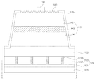
図1は、実施形態に係る発光素子を示す断面図で、図2は、図1のA−A線に沿って切断したオーミック層に対する平断面図である。 FIG. 1 is a cross-sectional view illustrating a light emitting device according to an embodiment, and FIG. 2 is a plan cross-sectional view with respect to an ohmic layer taken along the line AA in FIG.
図1を参照すれば、実施形態に係る発光素子100は、導電性基板110と、導電性基板110上に配置される第1電極層120と、第1電極層120上に配置される第1半導体層141、第2半導体層145、及び第1半導体層141と第2半導体層145との間に位置する活性層143を備える発光構造物140と、第2半導体層145と電気的に接続された第2電極層150とを含む。
Referring to FIG. 1, the light emitting device 100 according to the embodiment includes a
導電性基板110は、発光構造物140を支持し、第2電極層150と共に発光構造物140に電源を提供することができる。導電性基板110は、熱伝導性に優れた物質または伝導性物質で形成することができ、例えば、金(Au)、ニッケル(Ni)、タングステン(W)、モリブデン(Mo)、銅(Cu)、アルミニウム(Al)、タンタル(Ta)、銀(Ag)、白金(Pt)、クロム(Cr)、Si、Ge、GaAs、ZnO、GaN、Ga2O3またはSiC、SiGe、CuWから選択されるいずれか一つで形成したり、または二つ以上の合金で形成することができ、互いに異なる二つ以上の物質を積層して形成することができる。すなわち、導電性基板110はキャリアウエハとして具現してもよい。
The
このような導電性基板110は、発光素子100から発生する熱の放出を容易にして、発光素子100の熱的安定性を向上させることができる。
Such a
実施形態において、導電性基板110は、伝導性を有するものと説明するが、伝導性を有しなくてもよく、これに限定されない。
In the embodiment, the
導電性基板110上には発光構造物140に電源を供給する第1電極層120を含む。第1電極層120についての詳細な説明は後述する。
A
第1電極層120上には第1電極層120と発光構造物140との反射率の差を減少させるウィンドウ層130をさらに含むことができる。
A
ウィンドウ層130は、発光構造物140と第1電極層120との反射率の差を減少させることによって、光抽出効率を増加させる。
The
具体的に、ウィンドウ層130は、第1半導体層141と第1電極層120との間に位置する。
Specifically, the
ウィンドウ層130は、GaP、GaAsP及びAlGaAsのいずれか一つを含むことができる。
The
発光構造物140は、第1半導体層141、第2半導体層145、及び第1半導体層141と第2半導体層145との間の活性層143からなる。
The
第2半導体層145は、n型半導体層で具現することができ、n型半導体層は、例えば、InxAlyGa1−x−yN(0≦x≦1、0≦y≦1、0≦x+y≦1)の組成式を有する半導体材料、例えば、GaN、AlN、AlGaN、InGaN、InN、InAlGaN、AlInNなどから選択することができ、例えば、Si、Ge、Sn、Se、Teのようなn型ドーパントがドープされてもよい。また、第2半導体層145は、(AlXGa1−X)0.5In0.5Pの組成式を有する半導体材料から選択されてもよい。
The
一方、第2半導体層145上には第2半導体層145と電気的に接続された第2電極層150を配置することができ、第2電極層150は、少なくとも一つのパッドまたは/及び所定のパターンを有する電極を含むことができる。第2電極層150は、第2半導体層145の上面のうちセンター領域、外側領域または角領域に配置することができ、これに限定されない。第2電極層150は、第2半導体層145の上ではなく、他の領域に配置することができ、これに限定されない。
Meanwhile, a
第2電極層150は、伝導性物質、例えば、In、Co、Si、Ge、Au、Pd、Pt、Ru、Re、Mg、Zn、Hf、Ta、Rh、Ir、W、Ti、Ag、Cr、Mo、Nb、Al、Ni、Cu、及びWTiから選択された金属または合金を用いて、単層または多層に形成することができる。
The
第2電極層150が形成されていない第2半導体層145の表面の一部領域または全体領域に対して、所定のエッチング方法で、光抽出効率を向上させるための凹凸パターン160を形成することができる。
A concavo-
ここで、第2電極層150は、凹凸パターン160が形成されていない平坦な面に形成されたものと説明するが、凹凸パターン160が形成された上部面に形成されてもよく、これに限定されない。
Here, the
凹凸パターン160は、第2半導体層145の上面の少なくとも一領域に対してエッチングを行うことによって形成することができ、これに限定されない。エッチング過程は、湿式または/及び乾式エッチング工程を含み、エッチング過程を経ることによって、第2半導体層145の上面は凹凸パターン160を含むことができる。凹凸パターン160は、ランダムな大きさに不規則に形成してもよく、これに限定されない。凹凸パターン160は、平坦でない上面であって、テクスチャ(texture)パターン、凹凸パターン、平坦でないパターン(uneven pattern)のうち少なくとも一つを含むことができる。
The
凹凸パターン160は、側断面が円柱、多角柱、円錐、多角錐、円錐台、多角錐台などの様々な形状を有するように形成することができ、錐形状を含む。
The concavo-
一方、凹凸パターン160は、PEC(photo electro chemical)などの方法で形成することができ、これに限定されない。凹凸パターン160は、第2半導体層145の上部面に形成されることによって、活性層143から生成された光が第2半導体層145の上部面から全反射されて再吸収されたり、または散乱することを防止できるので、発光素子100の光抽出効率の向上に寄与することができる。
On the other hand, the
第2半導体層145の下には活性層143を形成することができる。活性層143は、電子と正孔が再結合される領域であって、電子と正孔が再結合することによって低いエネルギー準位に遷移し、それに相応する波長を有する光を生成することができる。
An
活性層143は、例えば、InxAlyGa1−x−yN(0≦x≦1、0≦y≦1、0≦x+y≦1)の組成式を有する半導体材料を含んで形成することができ、単一量子井戸構造または多重量子井戸構造(MQW:Multi Quantum Well)で形成することができる。また、活性層143は、(AlXGa1−X)0.5In0.5Pの組成式を有する半導体材料から選択されてもよい。
The
したがって、より多くの電子が量子井戸層の低いエネルギー準位に集まり、その結果、電子と正孔との再結合確率が増加して、発光効果を向上させることができる。また、量子線(Quantum wire)構造または量子点(Quantum dot)構造を含むこともできる。 Therefore, more electrons gather at the low energy level of the quantum well layer, and as a result, the recombination probability between electrons and holes increases, and the light emitting effect can be improved. Further, a quantum wire (Quantum wire) structure or a quantum dot (Quantum dot) structure may be included.
活性層143の下には第1半導体層141を形成することができる。第1半導体層141は、p型半導体層で具現されて、活性層143に正孔を注入することができる。例えば、p型半導体層は、InxAlyGa1−x−yN(0≦x≦1、0≦y≦1、0≦x+y≦1)の組成式を有する半導体材料、例えば、GaN、AlN、AlGaN、InGaN、InN、InAlGaN、AlInNなどから選択することができ、Mg、Zn、Ca、Sr、Baなどのp型ドーパントがドープされてもよい。また、第1半導体層141は、(AlXGa1−X)0.5In0.5Pの組成式を有する半導体材料から選択されてもよい。
A
また、第1半導体層141の下には第3半導体層(図示せず)を形成してもよい。ここで、第3半導体層は、第2半導体層と反対の極性を有する半導体層で具現することができる。
A third semiconductor layer (not shown) may be formed under the
一方、上述した第2半導体層145、活性層143及び第1半導体層141は、有機金属化学蒸着法(MOCVD;Metal Organic Chemical Vapor Deposition)、化学蒸着法(CVD;Chemical Vapor Deposition)、プラズマ化学蒸着法(PECVD;Plasma−Enhanced Chemical Vapor Deposition)、分子線成長法(MBE;Molecular Beam Epitaxy)、水素化物気相成長法(HVPE;Hydride Vapor Phase Epitaxy)、スパッタリング(Sputtering)などの方法を用いて形成することができ、これに限定されない。
On the other hand, the
また、上述したものとは異なり、実施形態において、第2半導体層145がp型半導体層で具現され、第1半導体層141がn型半導体層で具現されてもよいが、これに限定されない。これによって、発光構造物140は、N−P接合、P−N接合、N−P−N接合及びP−N−P接合構造のうち少なくとも一つを含むことができる。
In addition, unlike the above, in the embodiment, the
また、発光構造物140の外周面のうち一部領域または全体領域は、外部の衝撃などから保護し、電気的ショートを防止できるように、パッシベーション170が形成されてもよい。
In addition, a
図1及び図2を参照すれば、第1電極層120は、金属と透光性伝導層を選択的に使用することができ、発光構造物140に電源を提供する。第1電極層120は、伝導性材質を含んで形成することができる。例えば、ニッケル(Ni)、白金(Pt)、ルテニウム(Ru)、イリジウム(Ir)、ロジウム(Rh)、タンタル(Ta)、モリブデン(Mo)、チタン(Ti)、銀(Ag)、タングステン(W)、銅(Cu)、クロム(Cr)、パラジウム(Pd)、バナジウム(V)、コバルト(Co)、ニオブ(Nb)、ジルコニウム(Zr)、酸化インジウムスズ(ITO、indium tin oxide)、アルミニウム亜鉛酸化物(AZO、aluminum zinc oxide)、インジウム亜鉛酸化物(IZO、indium zinc oxide)、IZTO(indium zinc tin oxide)、IAZO(indium aluminum zinc oxide)、IGZO(indium gallium zinc oxide)、IGTO(indium gallium tin oxide)、ATO(antimony tin oxide)、GZO(gallium zinc oxide)、IrOx、RuOx、RuOx/ITO、Ni/IrOx/Au、またはNi/IrOx/Au/ITOのうち少なくとも一つで形成することができる。但し、これに限定されるものではない。
Referring to FIGS. 1 and 2, the
第1電極層120は、オーミック層123(ohmic layer)及び金属反射層125(reflective layer)のうち少なくとも一つを含むことができる。また、第1電極層120は、オーミック層123(ohmic layer)、金属反射層125(reflective layer)及び金属接着層121のうち少なくとも一つを含むことができる。
The
例えば、第1電極層120は、金属接着層121上に金属反射層125及びオーミック層123が順次積層された形態であってもよい。図1では、金属接着層121上にオーミック層123が積層された形態を示している。
For example, the
オーミック層123は、導電性基板110と発光構造物140との間に配置される透明電極層123Aと、透明電極層123Aを上下に貫通する多数個の金属コンタクト部123Bとを備えることができる。
The
透明電極層123Aは、導電性基板110または金属反射層125で反射される光が透過され、且つ導電性を有する材質であってもよい。例えば、透明電極層123Aは、In2O3、SnO2、ZnO、ITO、CTO、CuAlO2、CuGaO2及びSrCu2O2のうち少なくとも一つを含むことができる。
The
金属コンタクト部123Bは、透明電極層123Aを上下に貫通して多数配置される。多数個の金属コンタクト部123Bは、互いに規則的に離隔して配置される。金属コンタクト部123Bは発光構造物140とオーミックコンタクトされるようにする。
A large number of
また、金属コンタクト部123Bの少なくとも一面は発光構造物140の第1半導体層141に接し、他面は導電性基板110と接することができる。
In addition, at least one surface of the
金属コンタクト部123BはAuBeを含む。勿論、金属コンタクト部123BはAuまたはAu合金を含むこともできる。
The
金属コンタクト部123Bが透明電極層123Aを貫通して配置される場合、発光構造物140とのオーミック接触が容易になされるという利点がある。また、金属コンタクト部123Bが透明電極層123Aを貫通しているので、発光構造物140で発生する熱が導電性基板110に容易に排出されるという利点がある。
When the
また、金属コンタクト部123Bが発光構造物140と直接接触するので、VF(Voltage Forward)が低下するという利点がある。特に、金属コンタクト部123Bが透明電極層123Aを貫通しない場合と比較して、約10%程度の使用電圧が減少するという効果を有する。これは、透明電極層123Aは、金属コンタクト部123Bよりも伝導性が低いからである。
Further, since the
特に、図2を参照すれば、透明電極層123Aの平面上の面積は、金属コンタクト部123Bの平面上の面積よりも大きいことが好ましい。より好ましくは、金属コンタクト部123Bの平面上の面積は、透明電極層123Aの平面上の面積対比10%〜25%であればよい。金属コンタクト部123Bの平面上の面積は、透明電極層123Aの平面上の面積対比10%よりも小さい場合、発光構造物140と第1電極層120とのオーミック接触が難しく、金属コンタクト部123Bの平面上の面積は、透明電極層123Aの平面上の面積対比25%よりも大きい場合、光透過率が低い金属コンタクト部123Bのため、発光素子100の光効率が低下するという問題点がある。
In particular, referring to FIG. 2, the area of the
金属コンタクト部123Bの平面上の面積が、透明電極層123Aの平面上の面積対比10%〜25%となるためには、例えば、互いに隣接する金属コンタクト部123B間の離隔距離は35μm〜50μmであり、金属コンタクト部123Bの幅は10μm〜20μmであることが好ましい。
In order for the area on the plane of the
金属コンタクト部123Bの形状には特に制限がないが、棒状を有することができる。好ましくは、円柱または多角柱の形状を有する。
The shape of the
第1電極層120は、図1に示すようにフラットであってもよいが、これに限定されず、段差を有することができる。
The
第1電極層120は金属接着層121をさらに含むことができる。
The
金属接着層121は、オーミック層123の下に形成されて、層同士間の接着力を強化させることができる。金属接着層121は、下部物質との接着力に優れた物質を用いて形成することができる。例えば、PbSn合金、AuGe合金、AuBe合金、AuSn合金、Sn、In、SnIn合金及びPdIn合金のいずれか一つを含むことができる。
The
また、金属接着層121の上部に拡散防止膜(図示せず)をさらに形成することができる。拡散防止膜は、導電性基板110及び金属接着層121をなす物質が発光構造物140に拡散することを防止することができる。拡散防止膜は、金属の拡散を防止する物質で形成することができ、例えば、白金(Pt)、パラジウム(Pd)、タングステン(W)、ニッケル(Ni)、ルテニウム(Ru)、モリブデン(Mo)、イリジウム(Ir)、ロジウム(Rh)、タンタル(Ta)、ハフニウム(Hf)、ジルコニウム(Zr)、ニオブ(Nb)、バナジウム(V)のうち少なくとも一つまたは二つ以上の合金を用いることができる。但し、これに限定されるものではない。そして、金属接着層121は、単層または多層構造を有することができる。
In addition, a diffusion preventing film (not shown) can be further formed on the
図3は、本発明の他の一実施形態に係る発光素子を示す断面図である。 FIG. 3 is a cross-sectional view showing a light emitting device according to another embodiment of the present invention.
図3を参照すれば、実施形態に係る発光素子100Aは、図1の実施形態と比較すると、金属反射層125、及び電流遮断層180をさらに含む。
Referring to FIG. 3, the light emitting device 100 </ b> A according to the embodiment further includes a
第1電極層120は金属反射層125をさらに含む。金属反射層125は、オーミック層123の下に形成されて、活性層143で反射される光のうち導電性基板110に向かう光を発光構造物140の上部に反射させる。
The
金属反射層125は、反射特性に優れた物質、例えば、Ag、Ni、Al、Rh、Pd、Ir、Ru、Mg、Zn、Pt、AuまたはHf、またはこれらの選択的な組み合わせで構成された物質で形成されたり、または金属物質とIZO、IZTO、IAZO、IGZO、IGTO、AZO、ATOなどの透光性伝導性物質を用いて多層に形成することができる。また、反射層(図示せず)は、IZO/Ni、AZO/Ag、IZO/Ag/Ni、AZO/Ag/Niなどで積層することができる。
The
電流遮断層180は、発光構造物140の下に第2電極層150と垂直方向に少なくとも一領域が重なるように配置され、オーミック層123及び金属反射層125よりも低い電気伝導率を有することができる。電流遮断層180は、例えば、酸化アルミニウム(Al2O3)、酸化シリコン(SiO2)、窒化シリコン(Si3N4)、酸化チタン(TiOx)、酸化インジウムスズ(ITO、indium tin oxide)、アルミニウム亜鉛酸化物(AZO、aluminum zinc oxide)及びインジウム亜鉛酸化物(IZO、indium zinc oxide)のうち少なくとも一つを含むことができる。但し、これに限定されるものではない。
The
電流遮断層180は、高電流の印加時に第2半導体層145から活性層143に注入される電子が活性層143で再結合されずに第1電極層120に流れる現象を防止する電子遮断層(Electron blocking layer)であってもよい。電流遮断層180は、活性層143より相対的に大きいバンドギャップを有することによって、第2半導体層145から注入された電子が活性層143で再結合されずに第1半導体層141に注入される現象を防止することができる。これによって、活性層143で電子と正孔との再結合確率を高め、漏れ電流を防止することができる。
The
図4は、本発明の更に他の一実施形態に係る発光素子を示す断面図である。 FIG. 4 is a cross-sectional view showing a light emitting device according to another embodiment of the present invention.
図4を参照すれば、実施形態に係る発光素子100Bは、図1の実施形態と比較すると、ウィンドウ層130にドーピング領域133がさらに形成される点で異なる。
Referring to FIG. 4, the light emitting device 100 </ b> B according to the embodiment is different from the embodiment of FIG. 1 in that a
このとき、ウィンドウ層130は、金属コンタクト部123Bが接する領域に、不純物でドープされたドーピング領域133が形成され得る。
At this time, in the
ドーピング領域133は、金属コンタクト部123Bがウィンドウ層130に接する領域に形成され、好ましくは、第1半導体層141の極性と同一の極性のドーパントでドープされる。ここでは、第1半導体層141はp型ドーパントによりドープされることを前提とするので、ドーピング領域133はp型ドーパントによりドープされることを基準として説明する。
The
ウィンドウ層130がドープされる場合、光の透過度は減少するが、金属コンタクト部123Bとのオーミック接触をなす能力は上昇するようになる。したがって、ドーピング領域133が、ウィンドウ層130内で金属コンタクト部123Bと接する領域にのみ形成されるので、ウィンドウ層130と金属コンタクト部123Bとはオーミック接触するようになる。
When the
また、ウィンドウ層130内でドーピング領域133が減少することで、光透過性は大きく低下しない。結果的に、ウィンドウ層130におけるドーピング領域133の形成は、ウィンドウ層130の光透過率を大きく低下させないと共に、ウィンドウ層130と金属コンタクト部123Bとのオーミック接触を可能にする。
Further, since the
また、ウィンドウ層130と金属コンタクト部123Bとがオーミック接触することで、発光素子100の使用電圧は低くなり、ウィンドウ層130の光透過性が大きく低下しないので、発光効率は大きく低下しないという利点がある。
In addition, since the
ウィンドウ層130のドーピング領域133にドープされるp型ドーパントは、Mg、Zn、Ca、Sr、Ba及びCのいずれか一つを含むことができる。
The p-type dopant doped in the
ドーピング領域133が過度に高い濃度にドープされる場合、光透過率が著しく低下し、過度に低い濃度にドープされる場合、ウィンドウ層130と金属コンタクト部123Bとのオーミック接触が難しいことがある。したがって、ドーピング領域133がMgによりドープされる場合、ドーピング濃度は5×10¹⁸/cm3〜1×1018/cm3であり、Cによりドープされる場合、ドーピング濃度は5×1019/cm3〜1×1019/cm3であることが好ましい。
When the
ドーピング領域133は、ウィンドウ層130にドットまたは島形状に互いに離隔して配置される。ドーピング領域133の配置は金属コンタクト部123Bの配置に対応するので、以下では、金属コンタクト部123Bについてのみ説明する。
The
ドーピング領域133は、ウィンドウ層130の表面で一定の深さで形成されてもよい。また、ドーピング領域133は、ウィンドウ層130の表面から突出してもよい。すなわち、ウィンドウ層130の表面全体をドープし、ドーピング領域133を除外した領域をエッチングする過程でウィンドウ層130の表面がエッチングされて、ドーピング領域133がウィンドウ層130の表面から突出することができる。但し、これに限定されるものではない。
The
ドーピング領域133の平面上の面積は、上述した金属コンタクト部123Bの平面上の面積と同一に形成される。ドーピング領域133の平面上の面積が小さすぎると、ウィンドウ層130と金属コンタクト部123Bとがオーミック接触をなすことが難しく、広すぎると、発光素子の光効率が大きく低下する。
The area on the plane of the
もちろん、互いに隣接するドーピング領域133間の隔離距離も、金属コンタクト部123B間の隔離距離と同一にすることができる。
Of course, the separation distance between the
図5は、本発明の更に他の一実施形態に係る発光素子を示す断面図である。 FIG. 5 is a cross-sectional view showing a light emitting device according to another embodiment of the present invention.
図5を参照すれば、実施形態の発光素子100Cは、図3の実施形態と比較すると、ウィンドウ層130にドーピング領域133がさらに形成される点で異なる。
Referring to FIG. 5, the light emitting device 100 </ b> C of the embodiment is different from the embodiment of FIG. 3 in that a
ドーピング領域133についての説明は、上述した通りである。
The description of the
図6は、実施形態に係る発光素子を含む発光素子パッケージを示す斜視図で、図7は、実施形態に係る発光素子を含む発光素子パッケージを示す断面図である。 FIG. 6 is a perspective view illustrating a light emitting device package including the light emitting device according to the embodiment, and FIG. 7 is a cross-sectional view illustrating the light emitting device package including the light emitting device according to the embodiment.
図6及び図7を参照すれば、発光素子パッケージ500は、キャビティ520が形成されたボディー510と、ボディー510に実装される第1及び第2リードフレーム540,550と、第1及び第2リードフレーム540,550と電気的に接続される発光素子530と、発光素子530を覆うようにキャビティ520に充填される封止材(図示せず)とを含むことができる。
Referring to FIGS. 6 and 7, the light emitting
ボディー510は、ポリフタルアミド(PPA:Polyphthalamide)のような樹脂材質、シリコン(Si)、アルミニウム(Al)、窒化アルミニウム(AlN)、液晶ポリマー(PSG:photosensitive glass)、ポリアミド9T(PA9T)、シンジオタクチックポリスチレン(SPS)、金属材質、サファイア(Al2O3)、酸化ベリリウム(BeO)、印刷回路基板(PCB:Printed Circuit Board)のうち少なくとも一つで形成することができる。ボディー510は、射出成形、エッチング工程などにより形成することができるが、これに限定されない。
The
ボディー510の内側面は傾斜面とすることができる。このような傾斜面の角度によって、発光素子530から放出される光の反射角が変わり、これによって、外部に放出される光の指向角を調節することができる。
The inner surface of the
光の指向角が減るほど、発光素子530から外部に放出される光の集中性は増加し、逆に、光の指向角が大きいほど、発光素子530から外部に放出される光の集中性は減少する。
As the light directivity angle decreases, the concentration of light emitted from the
一方、ボディー510に形成されるキャビティ520を上から見た形状は、円形、四角形、多角形、楕円形などの形状であってもよく、角部を曲線にした形状であってもよいが、これに限定されるものではない。
On the other hand, the shape of the
発光素子530は、第1リードフレーム540上に実装され、例えば、赤色、緑色、青色、白色などの光を放出する発光素子、または紫外線を放出するUV(Ultra Violet)発光素子であってもよいが、これに限定されない。また、発光素子530は1個以上実装することができる。
The
また、発光素子530は、その電気端子が全て上部面に形成された水平タイプ(Horizontal type)、または上、下部面に形成された垂直タイプ(Vertical type)、またはフリップチップ(flip chip)のいずれにしてもよい。
In addition, the
封止材(図示せず)は、発光素子530を覆うようにキャビティ520に充填することができる。
A sealing material (not shown) can fill the
封止材(図示せず)は、シリコン、エポキシ、及びその他の樹脂材質で形成することができ、キャビティ520内に充填した後、それを紫外線または熱硬化する方式で形成することができる。
The sealing material (not shown) can be formed of silicon, epoxy, or other resin material, and can be formed by filling the
また、封止材(図示せず)は蛍光体を含むことができ、蛍光体は、発光素子530から放出される光の波長に応じてその種類が選択されて、発光素子パッケージ500が白色光を具現するようにすることができる。
Further, the sealing material (not shown) can include a phosphor, and the type of the phosphor is selected according to the wavelength of light emitted from the
このような蛍光体は、発光素子530から放出される光の波長に応じて、青色発光蛍光体、青緑色発光蛍光体、緑色発光蛍光体、黄緑色発光蛍光体、黄色発光蛍光体、黄赤色発光蛍光体、オレンジ色発光蛍光体、及び赤色発光蛍光体のいずれか一つを適用することができる。
Such phosphors are blue light-emitting phosphors, blue-green light-emitting phosphors, green light-emitting phosphors, yellow-green light-emitting phosphors, yellow light-emitting phosphors, yellow-red phosphors according to the wavelength of light emitted from the light-emitting
すなわち、蛍光体は、発光素子530から放出される第1光を有する光によって励起されて第2光を生成することができる。例えば、発光素子530が青色発光ダイオードで、蛍光体が黄色蛍光体である場合、黄色蛍光体は青色光によって励起されて黄色光を放出することができ、青色発光ダイオードで発生した青色光と、該青色光によって励起されて発生した黄色光とが混色されることで、発光素子パッケージ500は白色光を提供することができる。
That is, the phosphor can be excited by light having the first light emitted from the
これと同様に、発光素子530が緑色発光ダイオードである場合は、マゼンタ(magenta)蛍光体または青色と赤色の蛍光体を混用する場合を例に挙げることができ、発光素子530が赤色発光ダイオードである場合は、シアン(Cyan)蛍光体または青色と緑色蛍光体を混用する場合を例に挙げることができる。
Similarly, in the case where the
このような蛍光体は、YAG系、TAG系、硫化物系、シリケート系、アルミネート系、窒化物系、カーバイド系、ニトリドシリケート系、ホウ酸塩系、フッ化物系、リン酸塩系などの公知の蛍光体であってもよい。 Such phosphors include YAG, TAG, sulfide, silicate, aluminate, nitride, carbide, nitride silicate, borate, fluoride, phosphate, etc. The known phosphor may be used.
第1及び第2リードフレーム540,550は、金属材質、例えば、チタン(Ti)、銅(Cu)、ニッケル(Ni)、金(Au)、クロム(Cr)、タンタル(Ta)、白金(Pt)、錫(Sn)、銀(Ag)、リン(P)、アルミニウム(Al)、インジウム(In)、パラジウム(Pd)、コバルト(Co)、シリコン(Si)、ゲルマニウム(Ge)、ハフニウム(Hf)、ルテニウム(Ru)、鉄(Fe)のうち一つ以上の物質、またはこれらの合金を含むことができる。また、第1及び第2リードフレーム540、550は、単層または多層構造を有するように形成することができるが、これに限定されない。 The first and second lead frames 540 and 550 are made of a metal material such as titanium (Ti), copper (Cu), nickel (Ni), gold (Au), chromium (Cr), tantalum (Ta), platinum (Pt ), Tin (Sn), silver (Ag), phosphorus (P), aluminum (Al), indium (In), palladium (Pd), cobalt (Co), silicon (Si), germanium (Ge), hafnium (Hf) ), Ruthenium (Ru), iron (Fe), or an alloy thereof. In addition, the first and second lead frames 540 and 550 can be formed to have a single layer structure or a multilayer structure, but are not limited thereto.
第1及び第2リードフレーム540,550は、互いに離隔して電気的に分離される。発光素子530は、第1及び第2リードフレーム540、550上に実装され、第1及び第2リードフレーム540、550は発光素子530と直接接触したり、またははんだ付け(soldering)部材(図示せず)のような伝導性を有する材料を介して電気的に接続されてもよい。また、発光素子530は、ワイヤボンディングによって第1及び第2リードフレーム540、550と電気的に接続されてもよいが、これに限定されない。したがって、第1及び第2リードフレーム540、550に電源が連結されると、発光素子530に電源が印加され得る。一方、複数個のリードフレーム(図示せず)がボディー510内に実装され、それぞれのリードフレーム(図示せず)が発光素子530と電気的に接続されてもよいが、これに限定されない。
The first and second lead frames 540 and 550 are electrically separated from each other. The
図8は、実施形態に係る発光素子を含む照明装置を示す斜視図で、図9は、図8の照明装置のC−C'線断面図である。 FIG. 8 is a perspective view illustrating a lighting device including the light emitting element according to the embodiment, and FIG. 9 is a cross-sectional view taken along the line CC ′ of the lighting device of FIG.
図8及び図9を参照すれば、照明装置600は、ボディー610と、ボディー610と締結されるカバー630と、ボディー610の両端に位置するエンドキャップ650とを含むことができる。
Referring to FIGS. 8 and 9, the
ボディー610の下部面には発光素子モジュール640が締結され、ボディー610は、発光素子パッケージ644から発生した熱がボディー610の上部面を通じて外部に放出されるように、伝導性及び熱発散効果に優れた金属材質で形成することができる。
The light emitting
発光素子パッケージ644は、PCB 642上に多色、多列で実装されてアレイをなすことができ、同一の間隔で実装したり、または必要に応じて様々な離隔距離を有して実装できるので、明るさなどを調節することができる。このようなPCB 642としては、MPPCB(Metal Core PCB)またはFR4材質のPCBなどを用いることができる。
The light emitting
発光素子パッケージ644は、延長されたリードフレーム(図示せず)を含むことで、向上した放熱機能を有することができるので、発光素子パッケージ644の信頼性及び効率性を向上させることができ、発光素子パッケージ644及び発光素子パッケージ644を含む照明装置600の使用寿命を延長させることができる。
Since the light emitting
カバー630は、ボディー610の下部面を取り囲むように円形状に形成できるが、これに限定されないことは勿論である。
The
カバー630は、内部の発光素子モジュール640を外部の異物などから保護する。また、カバー630は、発光素子パッケージ644から発生した光のまぶしさを防止し、外部に光を均一に放出できるように拡散粒子を含むことができ、また、カバー630の内面及び外面のうち少なくともいずれか一面には、プリズムパターンなどを形成することができる。また、カバー630の内面及び外面のうち少なくともいずれか一面には蛍光体が塗布されてもよい。
The
一方、発光素子パッケージ644から発生した光はカバー630を通じて外部に放出されるので、カバー630は、優れた光透過率を有しなければならず、発光素子パッケージ644から発生した熱に耐えられるように、十分な耐熱性を備えなければならない。そのため、カバー630は、ポリエチレンテレフタレート(Polyethylen Terephthalate;PET)、ポリカーボネート(Polycarbonate;PC)またはポリメチルメタクリレート(Polymethyl Methacrylate;PMMA)などを含む材質で形成されることが好ましい。
On the other hand, since light generated from the light emitting
エンドキャップ650は、ボディー610の両端に位置し、電源装置(図示せず)を密閉する用途に使用することができる。また、エンドキャップ650には電源ピン652が形成されているので、実施形態に係る照明装置600は、既存の蛍光灯を除去した端子に別途の装置なしに直ぐ使用できるようになる。
The end caps 650 are positioned at both ends of the
図10は、実施形態に係る発光素子を含む液晶表示装置の分解斜視図である。 FIG. 10 is an exploded perspective view of a liquid crystal display device including the light emitting element according to the embodiment.
図10は、エッジ−ライト方式を示し、液晶表示装置700は、液晶表示パネル710と、液晶表示パネル710に光を提供するためのバックライトユニット770とを含むことができる。
FIG. 10 illustrates an edge-light method, and the liquid
液晶表示パネル710は、バックライトユニット770から提供される光を用いて画像を表示することができる。液晶表示パネル710は、液晶を挟んで互いに対向するカラーフィルタ基板712及び薄膜トランジスタ基板714を含むことができる。
The liquid crystal display panel 710 can display an image using light provided from the
カラーフィルタ基板712は、液晶表示パネル710を通じてディスプレイされる画像の色を具現することができる。
The
薄膜トランジスタ基板714は、駆動フィルム717を介して、多数の回路部品が実装される印刷回路基板718と電気的に接続されている。薄膜トランジスタ基板714は、印刷回路基板718から提供される駆動信号に応答して、印刷回路基板718から提供される駆動電圧を液晶に印加することができる。
The thin film transistor substrate 714 is electrically connected via a
薄膜トランジスタ基板714は、ガラスやプラスチックなどのような透明な材質の他の基板上に薄膜で形成された薄膜トランジスタ及び画素電極を含むことができる。 The thin film transistor substrate 714 may include a thin film transistor and a pixel electrode formed as a thin film on another substrate made of a transparent material such as glass or plastic.
バックライトユニット770は、光を出力する発光素子モジュール720と、発光素子モジュール720から提供される光を面光源の形態に変更させて液晶表示パネル710に提供する導光板730と、導光板730から提供された光の輝度分布を均一にし、垂直入射性を向上させる多数のフィルム752,766,764と、導光板730の後方に放出される光を導光板730へと反射させる反射シート747とで構成される。
The
発光素子モジュール720は、複数の発光素子パッケージ724と、複数の発光素子パッケージ724が実装されてアレイをなすためのPCB基板722とを含むことができる。この場合、曲がった発光素子パッケージ724の実装の信頼性を向上させることができる。
The light emitting device module 720 may include a plurality of light emitting device packages 724 and a PCB substrate 722 on which the plurality of light emitting device packages 724 are mounted to form an array. In this case, the mounting reliability of the bent light emitting
一方、バックライトユニット770は、導光板730から入射される光を液晶表示パネル710の方向に拡散させる拡散フィルム766と、拡散された光を集光して垂直入射性を向上させるプリズムフィルム752とで構成することができ、プリズムフィルム752を保護するための保護フィルム764を含むことができる。
Meanwhile, the
図11は、実施形態に係る発光素子を含む液晶表示装置の分解斜視図である。ただし、図10で図示し、説明した部分については反復して詳細に説明しない。 FIG. 11 is an exploded perspective view of a liquid crystal display device including the light emitting element according to the embodiment. However, the parts illustrated and described in FIG. 10 will not be described in detail repeatedly.
図11は、直下方式を示し、液晶表示装置800は、液晶表示パネル810と、液晶表示パネル810に光を提供するためのバックライトユニット870とを含むことができる。
FIG. 11 illustrates a direct method, and the liquid
液晶表示パネル810は、図10で説明した通りであり、詳細な説明は省略する。
The liquid
バックライトユニット870は、複数の発光素子モジュール823と、反射シート824と、発光素子モジュール823及び反射シート824が収納される下部シャーシ830と、発光素子モジュール823の上部に配置される拡散板840と、多数の光学フィルム860とを含むことができる。
The
発光素子モジュール823は、複数の発光素子パッケージ822と、複数の発光素子パッケージ822が実装されてアレイをなすためのPCB基板821とを含むことができる。
The light emitting device module 823 may include a plurality of light emitting device packages 822 and a
反射シート824は、発光素子パッケージ822から発生した光を、液晶表示パネル810が位置した方向に反射させることで、光の利用効率を向上させる。
The
一方、発光素子モジュール823から発生した光は拡散板840に入射し、拡散板840の上部には光学フィルム860が配置される。光学フィルム860は、拡散フィルム866、プリズムフィルム850及び保護フィルム864を含むことができる。
Meanwhile, light generated from the light emitting element module 823 is incident on the
以上、実施形態を中心に説明したが、これは単なる例示であり、本発明を限定するものではなく、本発明の属する分野における通常の知識を有する者であれば、本実施形態の本質的な特性を逸脱しない範囲で、以上で例示していない様々な変形及び応用が可能であるということが理解されるであろう。例えば、実施形態に具体的に示した各構成要素は変形実施が可能である。そして、このような変形及び応用に係る差異点は、添付の特許請求の範囲で規定する本発明の範囲に含まれるものと解釈しなければならない。 Although the embodiment has been mainly described above, this is merely an example and is not intended to limit the present invention. Any person having ordinary knowledge in the field to which the present invention belongs can be used. It will be understood that various modifications and applications not exemplified above are possible without departing from the characteristics. For example, each component specifically shown in the embodiment can be modified. Such differences in modification and application should be construed as being included in the scope of the present invention as defined in the appended claims.
Claims (7)
前記導電性基板上に配置される第1電極層と、
前記第1電極層上に配置される第1半導体層、第2半導体層、及び前記第1半導体層と前記第2半導体層との間に位置する活性層を備える発光構造物と、
前記第1電極層と前記第1半導体層との間に配置されて、前記第1電極層と前記第1半導体層との反射インデックスの差を減少させるウィンドウ層と、
前記第2半導体層と電気的に接続された第2電極層とを含み、
前記第1電極層は、
前記導電性基板と前記第1半導体層との間に配置される透明電極層と、
前記透明電極層を上下に貫通する多数個の金属コンタクト部とを備えるオーミック層を含み、
前記金属コンタクト部はAuBeを含み、
前記金属コンタクト部は、少なくとも一面が前記ウィンドウ層と接して、
前記ウィンドウ層は、前記金属コンタクト部が接する領域に、前記第1半導体層の極性と同一の極性のドーパントでドープされたドーピング領域を含み、
前記ドーピング領域は、ウィンドウ層内で金属コンタクトと接する領域にのみ形成され、
前記ドーピング領域の平面上の面積は、前記金属コンタクト部の平面上の面積と同一に形成される発光素子。 A conductive substrate;
A first electrode layer disposed on the conductive substrate;
A light emitting structure comprising: a first semiconductor layer disposed on the first electrode layer; a second semiconductor layer; and an active layer positioned between the first semiconductor layer and the second semiconductor layer;
A window layer disposed between the first electrode layer and the first semiconductor layer to reduce a difference in reflection index between the first electrode layer and the first semiconductor layer;
A second electrode layer electrically connected to the second semiconductor layer,
The first electrode layer includes
A transparent electrode layer disposed between the conductive substrate and the first semiconductor layer;
Including an ohmic layer comprising a plurality of metal contact portions vertically penetrating the transparent electrode layer,
The metal contact portion includes AuBe,
The metal contact portion, at least one surface in contact with the window layer,
The window layer includes a doping region doped with a dopant having the same polarity as the polarity of the first semiconductor layer in a region where the metal contact portion is in contact,
The doping region is formed only in a region in contact with the metal contact in the window layer;
The light emitting device has a planar area of the doping region that is the same as a planar area of the metal contact portion .
前記オーミック層の下に配置される金属反射層及び金属接着層をさらに含み、
前記金属接着層の一面は前記導電性基板と接する、請求項1乃至3のいずれかに記載の発光素子。 The first electrode layer includes
A metal reflective layer and a metal adhesive layer disposed under the ohmic layer;
4. The light emitting device according to claim 1, wherein one surface of the metal adhesive layer is in contact with the conductive substrate.
前記ドーピング領域がMgによりドープされる場合、ドーピング濃度は5×10¹⁸/cm3〜1×1018/cm3である、請求項1乃至5のいずれかに記載の発光素子。 The doped region is doped with a p-type dopant;
6. The light emitting device according to claim 1, wherein when the doping region is doped with Mg, a doping concentration is 5 × 10 18 / cm 3 to 1 × 10 18 / cm 3 .
前記ドーピング領域がCによりドープされる場合、ドーピング濃度は5×10¹⁹/cm3〜1×1019/cm3である、請求項1乃至5のいずれかに記載の発光素子。 The doped region is doped with a p-type dopant;
6. The light emitting device according to claim 1, wherein when the doping region is doped with C, a doping concentration is 5 × 10 19 / cm 3 to 1 × 10 19 / cm 3 .
Applications Claiming Priority (4)
| Application Number | Priority Date | Filing Date | Title |
|---|---|---|---|
| KR1020130010620A KR102035180B1 (en) | 2013-01-30 | 2013-01-30 | Light emitting device |
| KR10-2013-0010620 | 2013-01-30 | ||
| KR1020130092120A KR20150015983A (en) | 2013-08-02 | 2013-08-02 | Light emitting device |
| KR10-2013-0092120 | 2013-08-02 |
Publications (3)
| Publication Number | Publication Date |
|---|---|
| JP2014150255A JP2014150255A (en) | 2014-08-21 |
| JP2014150255A5 JP2014150255A5 (en) | 2016-12-08 |
| JP6385680B2 true JP6385680B2 (en) | 2018-09-05 |
Family
ID=50000912
Family Applications (1)
| Application Number | Title | Priority Date | Filing Date |
|---|---|---|---|
| JP2014015329A Active JP6385680B2 (en) | 2013-01-30 | 2014-01-30 | Light emitting element |
Country Status (5)
| Country | Link |
|---|---|
| US (1) | US8994058B2 (en) |
| EP (1) | EP2763194B1 (en) |
| JP (1) | JP6385680B2 (en) |
| CN (1) | CN103972362A (en) |
| TW (1) | TWI590493B (en) |
Families Citing this family (6)
| Publication number | Priority date | Publication date | Assignee | Title |
|---|---|---|---|---|
| WO2017026753A1 (en) * | 2015-08-07 | 2017-02-16 | 엘지이노텍 주식회사 | Light emitting diode and light emitting diode package |
| CN105322068B (en) * | 2015-11-17 | 2017-12-26 | 天津三安光电有限公司 | Light-emitting diode chip for backlight unit and preparation method thereof |
| JP6826395B2 (en) * | 2016-08-26 | 2021-02-03 | ローム株式会社 | Semiconductor light emitting device |
| CN110534659B (en) * | 2018-05-23 | 2022-09-27 | 昆明申北科技有限公司 | Anode structure of top-emitting OLED, display device and manufacturing method of display device |
| JP7360822B2 (en) | 2019-06-13 | 2023-10-13 | ローム株式会社 | semiconductor light emitting device |
| CN111009144A (en) * | 2019-12-11 | 2020-04-14 | 福州大学 | Traffic signal lamp based on micro LED |
Family Cites Families (22)
| Publication number | Priority date | Publication date | Assignee | Title |
|---|---|---|---|---|
| JP3981218B2 (en) * | 1999-04-28 | 2007-09-26 | 日立電線株式会社 | Epitaxial wafer for light emitting device and light emitting device |
| US6784462B2 (en) * | 2001-12-13 | 2004-08-31 | Rensselaer Polytechnic Institute | Light-emitting diode with planar omni-directional reflector |
| TW577178B (en) * | 2002-03-04 | 2004-02-21 | United Epitaxy Co Ltd | High efficient reflective metal layer of light emitting diode |
| US6716654B2 (en) * | 2002-03-12 | 2004-04-06 | Opto Tech Corporation | Light-emitting diode with enhanced brightness and method for fabricating the same |
| US8283683B2 (en) * | 2006-11-07 | 2012-10-09 | Opto Tech Corporation | Chip-bonding light emitting diode chip |
| JP5315070B2 (en) * | 2008-02-07 | 2013-10-16 | 昭和電工株式会社 | Compound semiconductor light emitting diode |
| JP2009200178A (en) * | 2008-02-20 | 2009-09-03 | Hitachi Cable Ltd | Semiconductor light-emitting device |
| US8008683B2 (en) * | 2008-10-22 | 2011-08-30 | Samsung Led Co., Ltd. | Semiconductor light emitting device |
| KR100969126B1 (en) * | 2009-03-10 | 2010-07-09 | 엘지이노텍 주식회사 | Light emitting device |
| KR101007140B1 (en) * | 2009-07-28 | 2011-01-10 | 엘지이노텍 주식회사 | Light emitting device |
| KR101039999B1 (en) * | 2010-02-08 | 2011-06-09 | 엘지이노텍 주식회사 | Semiconductor light emitting device and fabrication method thereof |
| KR100999798B1 (en) * | 2010-02-11 | 2010-12-08 | 엘지이노텍 주식회사 | Semiconductor light emitting device and fabrication method thereof |
| US8618565B2 (en) * | 2010-03-22 | 2013-12-31 | Seoul Opto Device Co., Ltd. | High efficiency light emitting diode |
| EP2442374B1 (en) * | 2010-10-12 | 2016-09-21 | LG Innotek Co., Ltd. | Light emitting device |
| EP2448015B1 (en) * | 2010-11-01 | 2018-04-11 | Samsung Electronics Co., Ltd. | Semiconductor light emitting device |
| KR101154320B1 (en) * | 2010-12-20 | 2012-06-13 | 엘지이노텍 주식회사 | Light emitting device, light emitting device package, and lighting device with the same |
| JP5050109B2 (en) * | 2011-03-14 | 2012-10-17 | 株式会社東芝 | Semiconductor light emitting device |
| JP2012222033A (en) * | 2011-04-05 | 2012-11-12 | Showa Denko Kk | Light-emitting diode manufacturing method and cutting method and light-emitting diode |
| JP5095840B2 (en) * | 2011-04-26 | 2012-12-12 | 株式会社東芝 | Semiconductor light emitting device |
| KR101868537B1 (en) * | 2011-11-07 | 2018-06-19 | 엘지이노텍 주식회사 | Light emitting device and light emitting device package including the device |
| JP2013179150A (en) * | 2012-02-28 | 2013-09-09 | Showa Denko Kk | Method for manufacturing light-emitting diode |
| KR20130120615A (en) * | 2012-04-26 | 2013-11-05 | 엘지이노텍 주식회사 | Light emitting device and light emitting device package |
-
2014
- 2014-01-29 TW TW103103375A patent/TWI590493B/en active
- 2014-01-29 CN CN201410043874.5A patent/CN103972362A/en active Pending
- 2014-01-29 EP EP14153003.0A patent/EP2763194B1/en active Active
- 2014-01-29 US US14/167,803 patent/US8994058B2/en active Active
- 2014-01-30 JP JP2014015329A patent/JP6385680B2/en active Active
Also Published As
| Publication number | Publication date |
|---|---|
| EP2763194A3 (en) | 2016-01-06 |
| TWI590493B (en) | 2017-07-01 |
| US20140209959A1 (en) | 2014-07-31 |
| EP2763194A2 (en) | 2014-08-06 |
| TW201438284A (en) | 2014-10-01 |
| EP2763194B1 (en) | 2018-03-07 |
| JP2014150255A (en) | 2014-08-21 |
| CN103972362A (en) | 2014-08-06 |
| US8994058B2 (en) | 2015-03-31 |
Similar Documents
| Publication | Publication Date | Title |
|---|---|---|
| JP6320769B2 (en) | Light emitting element | |
| JP6385680B2 (en) | Light emitting element | |
| KR20130013970A (en) | Light-emitting device | |
| JP6396023B2 (en) | Light emitting element | |
| KR102035180B1 (en) | Light emitting device | |
| KR20120133836A (en) | Light emitting device | |
| KR101907618B1 (en) | Light emitting device | |
| KR101863732B1 (en) | Light Emitting Device | |
| KR102075132B1 (en) | Light emitting device | |
| KR101807105B1 (en) | Light emitting device | |
| KR101838519B1 (en) | Light emitting device | |
| KR20120088985A (en) | Light Emitting device | |
| KR101722632B1 (en) | Light-emitting device | |
| KR20150015983A (en) | Light emitting device | |
| KR20140097900A (en) | Light emitting device | |
| KR20130059137A (en) | Light emitting device | |
| KR102065383B1 (en) | Light emitting device | |
| KR102057715B1 (en) | Light emitting device | |
| KR102042258B1 (en) | Light emitting device | |
| KR101813491B1 (en) | Light emitting device | |
| KR101843731B1 (en) | Light emitting device | |
| KR20130053344A (en) | Light emitting device | |
| KR20150084580A (en) | Light emitting device | |
| KR20120121188A (en) | Light emitting device | |
| KR20130009899A (en) | Light emitting device |
Legal Events
| Date | Code | Title | Description |
|---|---|---|---|
| A521 | Request for written amendment filed |
Free format text: JAPANESE INTERMEDIATE CODE: A523 Effective date: 20161024 |
|
| A621 | Written request for application examination |
Free format text: JAPANESE INTERMEDIATE CODE: A621 Effective date: 20161024 |
|
| A131 | Notification of reasons for refusal |
Free format text: JAPANESE INTERMEDIATE CODE: A131 Effective date: 20170912 |
|
| A977 | Report on retrieval |
Free format text: JAPANESE INTERMEDIATE CODE: A971007 Effective date: 20170913 |
|
| A521 | Request for written amendment filed |
Free format text: JAPANESE INTERMEDIATE CODE: A523 Effective date: 20171128 |
|
| A131 | Notification of reasons for refusal |
Free format text: JAPANESE INTERMEDIATE CODE: A131 Effective date: 20171219 |
|
| A521 | Request for written amendment filed |
Free format text: JAPANESE INTERMEDIATE CODE: A523 Effective date: 20180315 |
|
| TRDD | Decision of grant or rejection written | ||
| A01 | Written decision to grant a patent or to grant a registration (utility model) |
Free format text: JAPANESE INTERMEDIATE CODE: A01 Effective date: 20180710 |
|
| A61 | First payment of annual fees (during grant procedure) |
Free format text: JAPANESE INTERMEDIATE CODE: A61 Effective date: 20180808 |
|
| R150 | Certificate of patent or registration of utility model |
Ref document number: 6385680 Country of ref document: JP Free format text: JAPANESE INTERMEDIATE CODE: R150 |
|
| S531 | Written request for registration of change of domicile |
Free format text: JAPANESE INTERMEDIATE CODE: R313531 |
|
| R250 | Receipt of annual fees |
Free format text: JAPANESE INTERMEDIATE CODE: R250 |
|
| S111 | Request for change of ownership or part of ownership |
Free format text: JAPANESE INTERMEDIATE CODE: R313113 |
|
| R350 | Written notification of registration of transfer |
Free format text: JAPANESE INTERMEDIATE CODE: R350 |
|
| R350 | Written notification of registration of transfer |
Free format text: JAPANESE INTERMEDIATE CODE: R350 |
|
| R250 | Receipt of annual fees |
Free format text: JAPANESE INTERMEDIATE CODE: R250 |
|
| R250 | Receipt of annual fees |
Free format text: JAPANESE INTERMEDIATE CODE: R250 |