JP6385680B2 - 発光素子 - Google Patents
発光素子 Download PDFInfo
- Publication number
- JP6385680B2 JP6385680B2 JP2014015329A JP2014015329A JP6385680B2 JP 6385680 B2 JP6385680 B2 JP 6385680B2 JP 2014015329 A JP2014015329 A JP 2014015329A JP 2014015329 A JP2014015329 A JP 2014015329A JP 6385680 B2 JP6385680 B2 JP 6385680B2
- Authority
- JP
- Japan
- Prior art keywords
- layer
- light emitting
- emitting device
- electrode layer
- semiconductor layer
- Prior art date
- Legal status (The legal status is an assumption and is not a legal conclusion. Google has not performed a legal analysis and makes no representation as to the accuracy of the status listed.)
- Active
Links
Images


Classifications
-
- H—ELECTRICITY
- H01—ELECTRIC ELEMENTS
- H01L—SEMICONDUCTOR DEVICES NOT COVERED BY CLASS H10
- H01L33/00—Semiconductor devices with at least one potential-jump barrier or surface barrier specially adapted for light emission; Processes or apparatus specially adapted for the manufacture or treatment thereof or of parts thereof; Details thereof
- H01L33/36—Semiconductor devices with at least one potential-jump barrier or surface barrier specially adapted for light emission; Processes or apparatus specially adapted for the manufacture or treatment thereof or of parts thereof; Details thereof characterised by the electrodes
- H01L33/40—Materials therefor
- H01L33/42—Transparent materials
-
- H—ELECTRICITY
- H01—ELECTRIC ELEMENTS
- H01L—SEMICONDUCTOR DEVICES NOT COVERED BY CLASS H10
- H01L33/00—Semiconductor devices with at least one potential-jump barrier or surface barrier specially adapted for light emission; Processes or apparatus specially adapted for the manufacture or treatment thereof or of parts thereof; Details thereof
- H01L33/48—Semiconductor devices with at least one potential-jump barrier or surface barrier specially adapted for light emission; Processes or apparatus specially adapted for the manufacture or treatment thereof or of parts thereof; Details thereof characterised by the semiconductor body packages
- H01L33/62—Arrangements for conducting electric current to or from the semiconductor body, e.g. lead-frames, wire-bonds or solder balls
-
- H—ELECTRICITY
- H01—ELECTRIC ELEMENTS
- H01L—SEMICONDUCTOR DEVICES NOT COVERED BY CLASS H10
- H01L2224/00—Indexing scheme for arrangements for connecting or disconnecting semiconductor or solid-state bodies and methods related thereto as covered by H01L24/00
- H01L2224/01—Means for bonding being attached to, or being formed on, the surface to be connected, e.g. chip-to-package, die-attach, "first-level" interconnects; Manufacturing methods related thereto
- H01L2224/42—Wire connectors; Manufacturing methods related thereto
- H01L2224/47—Structure, shape, material or disposition of the wire connectors after the connecting process
- H01L2224/48—Structure, shape, material or disposition of the wire connectors after the connecting process of an individual wire connector
- H01L2224/4805—Shape
- H01L2224/4809—Loop shape
- H01L2224/48091—Arched
-
- H—ELECTRICITY
- H01—ELECTRIC ELEMENTS
- H01L—SEMICONDUCTOR DEVICES NOT COVERED BY CLASS H10
- H01L27/00—Devices consisting of a plurality of semiconductor or other solid-state components formed in or on a common substrate
- H01L27/15—Devices consisting of a plurality of semiconductor or other solid-state components formed in or on a common substrate including semiconductor components with at least one potential-jump barrier or surface barrier specially adapted for light emission
- H01L27/153—Devices consisting of a plurality of semiconductor or other solid-state components formed in or on a common substrate including semiconductor components with at least one potential-jump barrier or surface barrier specially adapted for light emission in a repetitive configuration, e.g. LED bars
- H01L27/156—Devices consisting of a plurality of semiconductor or other solid-state components formed in or on a common substrate including semiconductor components with at least one potential-jump barrier or surface barrier specially adapted for light emission in a repetitive configuration, e.g. LED bars two-dimensional arrays
-
- H—ELECTRICITY
- H01—ELECTRIC ELEMENTS
- H01L—SEMICONDUCTOR DEVICES NOT COVERED BY CLASS H10
- H01L2924/00—Indexing scheme for arrangements or methods for connecting or disconnecting semiconductor or solid-state bodies as covered by H01L24/00
- H01L2924/0001—Technical content checked by a classifier
- H01L2924/0002—Not covered by any one of groups H01L24/00, H01L24/00 and H01L2224/00
-
- H—ELECTRICITY
- H01—ELECTRIC ELEMENTS
- H01L—SEMICONDUCTOR DEVICES NOT COVERED BY CLASS H10
- H01L33/00—Semiconductor devices with at least one potential-jump barrier or surface barrier specially adapted for light emission; Processes or apparatus specially adapted for the manufacture or treatment thereof or of parts thereof; Details thereof
- H01L33/36—Semiconductor devices with at least one potential-jump barrier or surface barrier specially adapted for light emission; Processes or apparatus specially adapted for the manufacture or treatment thereof or of parts thereof; Details thereof characterised by the electrodes
- H01L33/38—Semiconductor devices with at least one potential-jump barrier or surface barrier specially adapted for light emission; Processes or apparatus specially adapted for the manufacture or treatment thereof or of parts thereof; Details thereof characterised by the electrodes with a particular shape
- H01L33/387—Semiconductor devices with at least one potential-jump barrier or surface barrier specially adapted for light emission; Processes or apparatus specially adapted for the manufacture or treatment thereof or of parts thereof; Details thereof characterised by the electrodes with a particular shape with a plurality of electrode regions in direct contact with the semiconductor body and being electrically interconnected by another electrode layer
-
- H—ELECTRICITY
- H01—ELECTRIC ELEMENTS
- H01L—SEMICONDUCTOR DEVICES NOT COVERED BY CLASS H10
- H01L33/00—Semiconductor devices with at least one potential-jump barrier or surface barrier specially adapted for light emission; Processes or apparatus specially adapted for the manufacture or treatment thereof or of parts thereof; Details thereof
- H01L33/36—Semiconductor devices with at least one potential-jump barrier or surface barrier specially adapted for light emission; Processes or apparatus specially adapted for the manufacture or treatment thereof or of parts thereof; Details thereof characterised by the electrodes
- H01L33/40—Materials therefor
- H01L33/405—Reflective materials
Description
Claims (7)
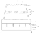
- 導電性基板と、
前記導電性基板上に配置される第1電極層と、
前記第1電極層上に配置される第1半導体層、第2半導体層、及び前記第1半導体層と前記第2半導体層との間に位置する活性層を備える発光構造物と、
前記第1電極層と前記第1半導体層との間に配置されて、前記第1電極層と前記第1半導体層との反射インデックスの差を減少させるウィンドウ層と、
前記第2半導体層と電気的に接続された第2電極層とを含み、
前記第1電極層は、
前記導電性基板と前記第1半導体層との間に配置される透明電極層と、
前記透明電極層を上下に貫通する多数個の金属コンタクト部とを備えるオーミック層を含み、
前記金属コンタクト部はAuBeを含み、
前記金属コンタクト部は、少なくとも一面が前記ウィンドウ層と接して、
前記ウィンドウ層は、前記金属コンタクト部が接する領域に、前記第1半導体層の極性と同一の極性のドーパントでドープされたドーピング領域を含み、
前記ドーピング領域は、ウィンドウ層内で金属コンタクトと接する領域にのみ形成され、
前記ドーピング領域の平面上の面積は、前記金属コンタクト部の平面上の面積と同一に形成される発光素子。 - 前記ドーピング領域は、前記ウィンドウ層の表面から突出する、請求項1に記載の発光素子。
- 前記透明電極層の平面上の面積は、前記金属コンタクト部の平面上の面積よりも大きい、請求項1又は2に記載の発光素子。
- 前記第1電極層は、
前記オーミック層の下に配置される金属反射層及び金属接着層をさらに含み、
前記金属接着層の一面は前記導電性基板と接する、請求項1乃至3のいずれかに記載の発光素子。 - 前記ウィンドウ層は、GaP、GaAsP及びAlGaAsのいずれか一つを含む、請求項1に記載の発光素子。
- 前記ドーピング領域はp型ドーパントによりドープされ、
前記ドーピング領域がMgによりドープされる場合、ドーピング濃度は5×10¹⁸/cm3〜1×1018/cm3である、請求項1乃至5のいずれかに記載の発光素子。 - 前記ドーピング領域はp型ドーパントによりドープされ、
前記ドーピング領域がCによりドープされる場合、ドーピング濃度は5×10¹⁹/cm3〜1×1019/cm3である、請求項1乃至5のいずれかに記載の発光素子。
Applications Claiming Priority (4)
| Application Number | Priority Date | Filing Date | Title |
|---|---|---|---|
| KR1020130010620A KR102035180B1 (ko) | 2013-01-30 | 2013-01-30 | 발광소자 |
| KR10-2013-0010620 | 2013-01-30 | ||
| KR1020130092120A KR20150015983A (ko) | 2013-08-02 | 2013-08-02 | 발광소자 |
| KR10-2013-0092120 | 2013-08-02 |
Publications (3)
| Publication Number | Publication Date |
|---|---|
| JP2014150255A JP2014150255A (ja) | 2014-08-21 |
| JP2014150255A5 JP2014150255A5 (ja) | 2016-12-08 |
| JP6385680B2 true JP6385680B2 (ja) | 2018-09-05 |
Family
ID=50000912
Family Applications (1)
| Application Number | Title | Priority Date | Filing Date |
|---|---|---|---|
| JP2014015329A Active JP6385680B2 (ja) | 2013-01-30 | 2014-01-30 | 発光素子 |
Country Status (5)
| Country | Link |
|---|---|
| US (1) | US8994058B2 (ja) |
| EP (1) | EP2763194B1 (ja) |
| JP (1) | JP6385680B2 (ja) |
| CN (1) | CN103972362A (ja) |
| TW (1) | TWI590493B (ja) |
Families Citing this family (6)
| Publication number | Priority date | Publication date | Assignee | Title |
|---|---|---|---|---|
| WO2017026753A1 (ko) | 2015-08-07 | 2017-02-16 | 엘지이노텍 주식회사 | 발광소자 및 발광소자 패키지 |
| CN105322068B (zh) * | 2015-11-17 | 2017-12-26 | 天津三安光电有限公司 | 发光二极管芯片及其制作方法 |
| JP6826395B2 (ja) * | 2016-08-26 | 2021-02-03 | ローム株式会社 | 半導体発光素子 |
| CN110534659B (zh) * | 2018-05-23 | 2022-09-27 | 昆明申北科技有限公司 | 顶发光oled的阳极结构、显示装置及其制造方法 |
| JP7360822B2 (ja) | 2019-06-13 | 2023-10-13 | ローム株式会社 | 半導体発光装置 |
| CN111009144A (zh) * | 2019-12-11 | 2020-04-14 | 福州大学 | 一种基于MicroLED的交通信号灯 |
Family Cites Families (22)
| Publication number | Priority date | Publication date | Assignee | Title |
|---|---|---|---|---|
| JP3981218B2 (ja) * | 1999-04-28 | 2007-09-26 | 日立電線株式会社 | 発光素子用エピタキシャルウエハおよび発光素子 |
| US6784462B2 (en) * | 2001-12-13 | 2004-08-31 | Rensselaer Polytechnic Institute | Light-emitting diode with planar omni-directional reflector |
| TW577178B (en) * | 2002-03-04 | 2004-02-21 | United Epitaxy Co Ltd | High efficient reflective metal layer of light emitting diode |
| US6716654B2 (en) * | 2002-03-12 | 2004-04-06 | Opto Tech Corporation | Light-emitting diode with enhanced brightness and method for fabricating the same |
| US8283683B2 (en) * | 2006-11-07 | 2012-10-09 | Opto Tech Corporation | Chip-bonding light emitting diode chip |
| JP5315070B2 (ja) * | 2008-02-07 | 2013-10-16 | 昭和電工株式会社 | 化合物半導体発光ダイオード |
| JP2009200178A (ja) * | 2008-02-20 | 2009-09-03 | Hitachi Cable Ltd | 半導体発光素子 |
| US8008683B2 (en) * | 2008-10-22 | 2011-08-30 | Samsung Led Co., Ltd. | Semiconductor light emitting device |
| KR100969126B1 (ko) * | 2009-03-10 | 2010-07-09 | 엘지이노텍 주식회사 | 발광 소자 |
| KR101007140B1 (ko) * | 2009-07-28 | 2011-01-10 | 엘지이노텍 주식회사 | 발광 소자 |
| KR101039999B1 (ko) * | 2010-02-08 | 2011-06-09 | 엘지이노텍 주식회사 | 반도체 발광소자 및 그 제조방법 |
| KR100999798B1 (ko) * | 2010-02-11 | 2010-12-08 | 엘지이노텍 주식회사 | 반도체 발광소자 및 그 제조방법 |
| US8618565B2 (en) * | 2010-03-22 | 2013-12-31 | Seoul Opto Device Co., Ltd. | High efficiency light emitting diode |
| TWI532214B (zh) * | 2010-10-12 | 2016-05-01 | Lg伊諾特股份有限公司 | 發光元件及其封裝 |
| EP2448015B1 (en) * | 2010-11-01 | 2018-04-11 | Samsung Electronics Co., Ltd. | Semiconductor light emitting device |
| KR101154320B1 (ko) * | 2010-12-20 | 2012-06-13 | 엘지이노텍 주식회사 | 발광소자, 발광소자 패키지 및 이를 포함하는 조명 장치 |
| JP5050109B2 (ja) * | 2011-03-14 | 2012-10-17 | 株式会社東芝 | 半導体発光素子 |
| JP2012222033A (ja) * | 2011-04-05 | 2012-11-12 | Showa Denko Kk | 発光ダイオードの製造方法、切断方法及び発光ダイオード |
| JP5095840B2 (ja) * | 2011-04-26 | 2012-12-12 | 株式会社東芝 | 半導体発光素子 |
| KR101868537B1 (ko) * | 2011-11-07 | 2018-06-19 | 엘지이노텍 주식회사 | 발광소자 및 이를 포함하는 발광 소자 패키지 |
| JP2013179150A (ja) * | 2012-02-28 | 2013-09-09 | Showa Denko Kk | 発光ダイオードの製造方法 |
| KR20130120615A (ko) * | 2012-04-26 | 2013-11-05 | 엘지이노텍 주식회사 | 발광 소자 및 발광 소자 패키지 |
-
2014
- 2014-01-29 US US14/167,803 patent/US8994058B2/en active Active
- 2014-01-29 EP EP14153003.0A patent/EP2763194B1/en active Active
- 2014-01-29 CN CN201410043874.5A patent/CN103972362A/zh active Pending
- 2014-01-29 TW TW103103375A patent/TWI590493B/zh active
- 2014-01-30 JP JP2014015329A patent/JP6385680B2/ja active Active
Also Published As
| Publication number | Publication date |
|---|---|
| TW201438284A (zh) | 2014-10-01 |
| US8994058B2 (en) | 2015-03-31 |
| EP2763194B1 (en) | 2018-03-07 |
| TWI590493B (zh) | 2017-07-01 |
| US20140209959A1 (en) | 2014-07-31 |
| EP2763194A2 (en) | 2014-08-06 |
| EP2763194A3 (en) | 2016-01-06 |
| JP2014150255A (ja) | 2014-08-21 |
| CN103972362A (zh) | 2014-08-06 |
Similar Documents
| Publication | Publication Date | Title |
|---|---|---|
| JP6320769B2 (ja) | 発光素子 | |
| JP6385680B2 (ja) | 発光素子 | |
| KR20130013970A (ko) | 발광소자 패키지 | |
| JP6396023B2 (ja) | 発光素子 | |
| KR102035180B1 (ko) | 발광소자 | |
| KR20120133836A (ko) | 발광소자 | |
| KR101907618B1 (ko) | 발광소자 | |
| KR101863732B1 (ko) | 발광소자 | |
| KR102075132B1 (ko) | 발광소자 | |
| KR101807105B1 (ko) | 발광소자 | |
| KR101838519B1 (ko) | 발광소자 | |
| KR20120088985A (ko) | 발광소자 | |
| KR101722632B1 (ko) | 발광소자패키지 | |
| KR20150015983A (ko) | 발광소자 | |
| KR20140097900A (ko) | 발광소자 | |
| KR20130059137A (ko) | 발광소자 | |
| KR102065383B1 (ko) | 발광소자 | |
| KR102057715B1 (ko) | 발광소자 | |
| KR102042258B1 (ko) | 발광소자 | |
| KR101813491B1 (ko) | 발광 소자 | |
| KR101843731B1 (ko) | 발광소자 | |
| KR20130053344A (ko) | 발광소자 | |
| KR20150084580A (ko) | 발광소자 | |
| KR20120121188A (ko) | 발광소자 | |
| KR20130009899A (ko) | 발광소자 |
Legal Events
| Date | Code | Title | Description |
|---|---|---|---|
| A521 | Request for written amendment filed |
Free format text: JAPANESE INTERMEDIATE CODE: A523 Effective date: 20161024 |
|
| A621 | Written request for application examination |
Free format text: JAPANESE INTERMEDIATE CODE: A621 Effective date: 20161024 |
|
| A131 | Notification of reasons for refusal |
Free format text: JAPANESE INTERMEDIATE CODE: A131 Effective date: 20170912 |
|
| A977 | Report on retrieval |
Free format text: JAPANESE INTERMEDIATE CODE: A971007 Effective date: 20170913 |
|
| A521 | Request for written amendment filed |
Free format text: JAPANESE INTERMEDIATE CODE: A523 Effective date: 20171128 |
|
| A131 | Notification of reasons for refusal |
Free format text: JAPANESE INTERMEDIATE CODE: A131 Effective date: 20171219 |
|
| A521 | Request for written amendment filed |
Free format text: JAPANESE INTERMEDIATE CODE: A523 Effective date: 20180315 |
|
| TRDD | Decision of grant or rejection written | ||
| A01 | Written decision to grant a patent or to grant a registration (utility model) |
Free format text: JAPANESE INTERMEDIATE CODE: A01 Effective date: 20180710 |
|
| A61 | First payment of annual fees (during grant procedure) |
Free format text: JAPANESE INTERMEDIATE CODE: A61 Effective date: 20180808 |
|
| R150 | Certificate of patent or registration of utility model |
Ref document number: 6385680 Country of ref document: JP Free format text: JAPANESE INTERMEDIATE CODE: R150 |
|
| S531 | Written request for registration of change of domicile |
Free format text: JAPANESE INTERMEDIATE CODE: R313531 |
|
| R250 | Receipt of annual fees |
Free format text: JAPANESE INTERMEDIATE CODE: R250 |
|
| S111 | Request for change of ownership or part of ownership |
Free format text: JAPANESE INTERMEDIATE CODE: R313113 |
|
| R350 | Written notification of registration of transfer |
Free format text: JAPANESE INTERMEDIATE CODE: R350 |
|
| R350 | Written notification of registration of transfer |
Free format text: JAPANESE INTERMEDIATE CODE: R350 |
|
| R250 | Receipt of annual fees |
Free format text: JAPANESE INTERMEDIATE CODE: R250 |
|
| R250 | Receipt of annual fees |
Free format text: JAPANESE INTERMEDIATE CODE: R250 |