JP5208436B2 - チップ抵抗器の製造方法 - Google Patents
チップ抵抗器の製造方法 Download PDFInfo
- Publication number
- JP5208436B2 JP5208436B2 JP2007074736A JP2007074736A JP5208436B2 JP 5208436 B2 JP5208436 B2 JP 5208436B2 JP 2007074736 A JP2007074736 A JP 2007074736A JP 2007074736 A JP2007074736 A JP 2007074736A JP 5208436 B2 JP5208436 B2 JP 5208436B2
- Authority
- JP
- Japan
- Prior art keywords
- easy
- cut
- substrate
- chip resistor
- grooves
- Prior art date
- Legal status (The legal status is an assumption and is not a legal conclusion. Google has not performed a legal analysis and makes no representation as to the accuracy of the status listed.)
- Expired - Fee Related
Links
- 238000004519 manufacturing process Methods 0.000 title claims description 22
- 239000000758 substrate Substances 0.000 claims description 51
- 238000000034 method Methods 0.000 claims description 12
- 239000000463 material Substances 0.000 claims description 4
- 230000007423 decrease Effects 0.000 claims description 2
- 238000005452 bending Methods 0.000 description 8
- 239000004020 conductor Substances 0.000 description 7
- 239000012467 final product Substances 0.000 description 5
- 229910045601 alloy Inorganic materials 0.000 description 3
- 239000000956 alloy Substances 0.000 description 3
- 229910017566 Cu-Mn Inorganic materials 0.000 description 1
- 229910017871 Cu—Mn Inorganic materials 0.000 description 1
- 229910018054 Ni-Cu Inorganic materials 0.000 description 1
- 229910018487 Ni—Cr Inorganic materials 0.000 description 1
- 229910018481 Ni—Cu Inorganic materials 0.000 description 1
- 238000010304 firing Methods 0.000 description 1
- 238000007747 plating Methods 0.000 description 1
Images


Landscapes
- Apparatuses And Processes For Manufacturing Resistors (AREA)
Description
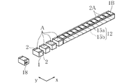
Bl 分割ブロック
Rl 分割ローラ
x (第1)方向
y (第2)方向
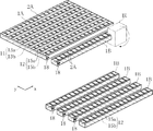
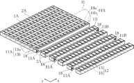
1 抵抗体
1A 基板
1B 帯状部材
2 電極
2A 導電体層
11,11A,11B 第1切断容易部
12 第2切断容易部
13a,13b,14a,14b,15a,15b 溝
18 最終破断面
Claims (2)
- 抵抗体材料からなり、第1方向に延びる複数の第1切断容易部と、上記第1方向と直角である第2方向に延びる複数の第2切断容易部と、を有する基板を形成する工程と、
上記基板を上記複数の第1切断容易部に沿って切断することにより、複数の帯状部材に分割する工程と、
上記帯状部材を上記複数の第2切断容易部に沿って切断することにより、複数のチップ抵抗器に分割する工程と、
を有するチップ抵抗器の製造方法であって、
上記第1切断容易部は、上記基板の表面側および裏面側の少なくともいずれかに形成された溝からなり、
上記溝の深さが、上記第1切断容易部が延びる方向において一方から他方に向けて単調増加または単調減少していることを特徴とする、チップ抵抗器の製造方法。 - 上記第2方向において隣り合う上記第1切断容易部どうしは、それぞれを構成する上記溝の深さの傾斜方向が反対とされている、請求項1に記載のチップ抵抗器の製造方法。
Priority Applications (1)
| Application Number | Priority Date | Filing Date | Title |
|---|---|---|---|
| JP2007074736A JP5208436B2 (ja) | 2007-03-22 | 2007-03-22 | チップ抵抗器の製造方法 |
Applications Claiming Priority (1)
| Application Number | Priority Date | Filing Date | Title |
|---|---|---|---|
| JP2007074736A JP5208436B2 (ja) | 2007-03-22 | 2007-03-22 | チップ抵抗器の製造方法 |
Publications (2)
| Publication Number | Publication Date |
|---|---|
| JP2008235670A JP2008235670A (ja) | 2008-10-02 |
| JP5208436B2 true JP5208436B2 (ja) | 2013-06-12 |
Family
ID=39908098
Family Applications (1)
| Application Number | Title | Priority Date | Filing Date |
|---|---|---|---|
| JP2007074736A Expired - Fee Related JP5208436B2 (ja) | 2007-03-22 | 2007-03-22 | チップ抵抗器の製造方法 |
Country Status (1)
| Country | Link |
|---|---|
| JP (1) | JP5208436B2 (ja) |
Families Citing this family (3)
| Publication number | Priority date | Publication date | Assignee | Title |
|---|---|---|---|---|
| JP5543146B2 (ja) | 2009-07-27 | 2014-07-09 | ローム株式会社 | チップ抵抗器およびチップ抵抗器の製造方法 |
| JP5791450B2 (ja) * | 2011-09-28 | 2015-10-07 | 京セラ株式会社 | 多数個取り配線基板および配線基板 |
| CN116631716A (zh) * | 2023-07-18 | 2023-08-22 | 合肥矽迈微电子科技有限公司 | 一种可变电阻器件的制作方法 |
Family Cites Families (4)
| Publication number | Priority date | Publication date | Assignee | Title |
|---|---|---|---|---|
| JPH04509U (ja) * | 1990-04-17 | 1992-01-06 | ||
| JP3029821B2 (ja) * | 1998-06-04 | 2000-04-10 | ローム株式会社 | 電子部品用基板 |
| JP2000238034A (ja) * | 1999-02-18 | 2000-09-05 | Rohm Co Ltd | セラミックス基板及び同セラミックス基板の分割方法 |
| JP2007049071A (ja) * | 2005-08-12 | 2007-02-22 | Rohm Co Ltd | チップ抵抗器とその製造方法 |
-
2007
- 2007-03-22 JP JP2007074736A patent/JP5208436B2/ja not_active Expired - Fee Related
Also Published As
| Publication number | Publication date |
|---|---|
| JP2008235670A (ja) | 2008-10-02 |
Similar Documents
| Publication | Publication Date | Title |
|---|---|---|
| KR101536068B1 (ko) | 배선기판, 다수개 취득 배선기판, 및 그 제조방법 | |
| JP5208436B2 (ja) | チップ抵抗器の製造方法 | |
| JP7606449B2 (ja) | 窒化ケイ素基板の製造方法及び窒化ケイ素基材 | |
| WO2012144114A1 (ja) | 配線基板、多数個取り配線基板、およびその製造方法 | |
| WO2004001774A1 (ja) | 低い抵抗値を有するチップ抵抗器とその製造方法 | |
| TWI534841B (zh) | Method of manufacturing wafer resistors | |
| JP5812207B2 (ja) | フレキシブル多層基板 | |
| US9942995B2 (en) | Method for producing a metal core substrate having improved edge insulating properties | |
| US8455769B2 (en) | Electronic component and method of mounting the same | |
| JP5014767B2 (ja) | チップ抵抗器の製造方法 | |
| JP4277633B2 (ja) | チップ抵抗器の製造方法 | |
| JP6892339B2 (ja) | 抵抗器 | |
| JP3954080B2 (ja) | 多層プリント配線板の製造方法 | |
| JP2007049071A (ja) | チップ抵抗器とその製造方法 | |
| JP4788410B2 (ja) | セラミック積層基板の製造方法 | |
| JP4881557B2 (ja) | チップ抵抗器の製造方法 | |
| JP5891342B2 (ja) | チップ抵抗器の製造方法 | |
| JP6749752B2 (ja) | チップ抵抗器およびチップ抵抗器の製造方法 | |
| JP4542967B2 (ja) | チップ抵抗器の製造方法 | |
| JP2004088027A (ja) | 集合電子部品、セラミック電子部品およびセラミック電子部品の製造方法 | |
| JP3837091B2 (ja) | 低い抵抗値を有するチップ抵抗器とその製造方法 | |
| JP4867325B2 (ja) | チップ形ネットワーク電子部品の製造方法 | |
| JP4978230B2 (ja) | ジャンパーチップ部品およびその製造方法 | |
| JP2020098806A (ja) | チップ抵抗器およびその製造方法 | |
| JP2026068814A (ja) | 金属加工品の製造方法 |
Legal Events
| Date | Code | Title | Description |
|---|---|---|---|
| A621 | Written request for application examination |
Free format text: JAPANESE INTERMEDIATE CODE: A621 Effective date: 20100122 |
|
| A977 | Report on retrieval |
Free format text: JAPANESE INTERMEDIATE CODE: A971007 Effective date: 20120717 |
|
| A131 | Notification of reasons for refusal |
Free format text: JAPANESE INTERMEDIATE CODE: A131 Effective date: 20120724 |
|
| A521 | Written amendment |
Free format text: JAPANESE INTERMEDIATE CODE: A523 Effective date: 20120920 |
|
| A131 | Notification of reasons for refusal |
Free format text: JAPANESE INTERMEDIATE CODE: A131 Effective date: 20121204 |
|
| A521 | Written amendment |
Free format text: JAPANESE INTERMEDIATE CODE: A523 Effective date: 20130201 |
|
| TRDD | Decision of grant or rejection written | ||
| A01 | Written decision to grant a patent or to grant a registration (utility model) |
Free format text: JAPANESE INTERMEDIATE CODE: A01 Effective date: 20130219 |
|
| A61 | First payment of annual fees (during grant procedure) |
Free format text: JAPANESE INTERMEDIATE CODE: A61 Effective date: 20130220 |
|
| FPAY | Renewal fee payment (event date is renewal date of database) |
Free format text: PAYMENT UNTIL: 20160301 Year of fee payment: 3 |
|
| R150 | Certificate of patent or registration of utility model |
Ref document number: 5208436 Country of ref document: JP Free format text: JAPANESE INTERMEDIATE CODE: R150 Free format text: JAPANESE INTERMEDIATE CODE: R150 |
|
| LAPS | Cancellation because of no payment of annual fees |