JP5205724B2 - Light emitting device - Google Patents
Light emitting device Download PDFInfo
- Publication number
- JP5205724B2 JP5205724B2 JP2006213929A JP2006213929A JP5205724B2 JP 5205724 B2 JP5205724 B2 JP 5205724B2 JP 2006213929 A JP2006213929 A JP 2006213929A JP 2006213929 A JP2006213929 A JP 2006213929A JP 5205724 B2 JP5205724 B2 JP 5205724B2
- Authority
- JP
- Japan
- Prior art keywords
- light
- light emitting
- recess
- emitting device
- emitting element
- Prior art date
- Legal status (The legal status is an assumption and is not a legal conclusion. Google has not performed a legal analysis and makes no representation as to the accuracy of the status listed.)
- Active
Links
- 238000007789 sealing Methods 0.000 claims abstract description 113
- 239000003566 sealing material Substances 0.000 claims abstract description 79
- 239000000654 additive Substances 0.000 claims abstract description 75
- 229920005989 resin Polymers 0.000 claims abstract description 66
- 239000011347 resin Substances 0.000 claims abstract description 66
- OAICVXFJPJFONN-UHFFFAOYSA-N Phosphorus Chemical compound [P] OAICVXFJPJFONN-UHFFFAOYSA-N 0.000 claims description 73
- 230000000996 additive effect Effects 0.000 claims description 64
- 239000002245 particle Substances 0.000 claims description 63
- 229920002050 silicone resin Polymers 0.000 claims description 20
- 238000000149 argon plasma sintering Methods 0.000 claims description 7
- 230000000903 blocking effect Effects 0.000 abstract description 5
- 239000000463 material Substances 0.000 description 28
- 230000004048 modification Effects 0.000 description 19
- 238000012986 modification Methods 0.000 description 19
- 230000000694 effects Effects 0.000 description 18
- 230000001681 protective effect Effects 0.000 description 16
- 230000006866 deterioration Effects 0.000 description 13
- 239000004065 semiconductor Substances 0.000 description 12
- 229910052693 Europium Inorganic materials 0.000 description 10
- 239000012535 impurity Substances 0.000 description 9
- 239000000853 adhesive Substances 0.000 description 8
- 230000001070 adhesive effect Effects 0.000 description 8
- 229910052791 calcium Inorganic materials 0.000 description 8
- 229910052747 lanthanoid Inorganic materials 0.000 description 8
- 150000002602 lanthanoids Chemical class 0.000 description 8
- 229920000647 polyepoxide Polymers 0.000 description 8
- 229910052712 strontium Inorganic materials 0.000 description 8
- 229910052788 barium Inorganic materials 0.000 description 7
- 239000003822 epoxy resin Substances 0.000 description 7
- 229910052725 zinc Inorganic materials 0.000 description 7
- 229910052684 Cerium Inorganic materials 0.000 description 6
- RYGMFSIKBFXOCR-UHFFFAOYSA-N Copper Chemical compound [Cu] RYGMFSIKBFXOCR-UHFFFAOYSA-N 0.000 description 6
- XEEYBQQBJWHFJM-UHFFFAOYSA-N Iron Chemical compound [Fe] XEEYBQQBJWHFJM-UHFFFAOYSA-N 0.000 description 6
- 229910052802 copper Inorganic materials 0.000 description 6
- 239000010949 copper Substances 0.000 description 6
- 229910052749 magnesium Inorganic materials 0.000 description 6
- 238000004519 manufacturing process Methods 0.000 description 6
- 238000000034 method Methods 0.000 description 6
- 238000000926 separation method Methods 0.000 description 6
- 239000000126 substance Substances 0.000 description 6
- 230000007423 decrease Effects 0.000 description 5
- 229910052761 rare earth metal Inorganic materials 0.000 description 5
- 238000004062 sedimentation Methods 0.000 description 5
- VYPSYNLAJGMNEJ-UHFFFAOYSA-N Silicium dioxide Chemical compound O=[Si]=O VYPSYNLAJGMNEJ-UHFFFAOYSA-N 0.000 description 4
- 229910052784 alkaline earth metal Inorganic materials 0.000 description 4
- 229910052782 aluminium Inorganic materials 0.000 description 4
- XAGFODPZIPBFFR-UHFFFAOYSA-N aluminium Chemical compound [Al] XAGFODPZIPBFFR-UHFFFAOYSA-N 0.000 description 4
- 229910052751 metal Inorganic materials 0.000 description 4
- 239000002184 metal Substances 0.000 description 4
- 150000004767 nitrides Chemical class 0.000 description 4
- -1 Alkaline earth metal aluminate Chemical class 0.000 description 3
- 229910052688 Gadolinium Inorganic materials 0.000 description 3
- MUBZPKHOEPUJKR-UHFFFAOYSA-N Oxalic acid Chemical compound OC(=O)C(O)=O MUBZPKHOEPUJKR-UHFFFAOYSA-N 0.000 description 3
- 239000004954 Polyphthalamide Substances 0.000 description 3
- GWEVSGVZZGPLCZ-UHFFFAOYSA-N Titan oxide Chemical compound O=[Ti]=O GWEVSGVZZGPLCZ-UHFFFAOYSA-N 0.000 description 3
- 150000001342 alkaline earth metals Chemical class 0.000 description 3
- 229910052794 bromium Inorganic materials 0.000 description 3
- 229910052801 chlorine Inorganic materials 0.000 description 3
- 239000003086 colorant Substances 0.000 description 3
- 238000009826 distribution Methods 0.000 description 3
- 239000008393 encapsulating agent Substances 0.000 description 3
- 238000000605 extraction Methods 0.000 description 3
- 229910052731 fluorine Inorganic materials 0.000 description 3
- 229910052736 halogen Inorganic materials 0.000 description 3
- 150000002367 halogens Chemical class 0.000 description 3
- 229910052742 iron Inorganic materials 0.000 description 3
- 229910052748 manganese Inorganic materials 0.000 description 3
- 229920006375 polyphtalamide Polymers 0.000 description 3
- 229910052709 silver Inorganic materials 0.000 description 3
- 238000002834 transmittance Methods 0.000 description 3
- 238000004383 yellowing Methods 0.000 description 3
- 229910052727 yttrium Inorganic materials 0.000 description 3
- 229920000106 Liquid crystal polymer Polymers 0.000 description 2
- 239000004977 Liquid-crystal polymers (LCPs) Substances 0.000 description 2
- BPQQTUXANYXVAA-UHFFFAOYSA-N Orthosilicate Chemical compound [O-][Si]([O-])([O-])[O-] BPQQTUXANYXVAA-UHFFFAOYSA-N 0.000 description 2
- BQCADISMDOOEFD-UHFFFAOYSA-N Silver Chemical compound [Ag] BQCADISMDOOEFD-UHFFFAOYSA-N 0.000 description 2
- UCKMPCXJQFINFW-UHFFFAOYSA-N Sulphide Chemical compound [S-2] UCKMPCXJQFINFW-UHFFFAOYSA-N 0.000 description 2
- 229910052771 Terbium Inorganic materials 0.000 description 2
- UHAQRCJYQAKQEE-UHFFFAOYSA-M [O-2].[OH-].O.[Al+3].P Chemical compound [O-2].[OH-].O.[Al+3].P UHAQRCJYQAKQEE-UHFFFAOYSA-M 0.000 description 2
- 150000004645 aluminates Chemical class 0.000 description 2
- PNEYBMLMFCGWSK-UHFFFAOYSA-N aluminium oxide Inorganic materials [O-2].[O-2].[O-2].[Al+3].[Al+3] PNEYBMLMFCGWSK-UHFFFAOYSA-N 0.000 description 2
- 229910052586 apatite Inorganic materials 0.000 description 2
- 230000008901 benefit Effects 0.000 description 2
- 238000000295 emission spectrum Methods 0.000 description 2
- 238000005538 encapsulation Methods 0.000 description 2
- 239000011521 glass Substances 0.000 description 2
- PCHJSUWPFVWCPO-UHFFFAOYSA-N gold Chemical compound [Au] PCHJSUWPFVWCPO-UHFFFAOYSA-N 0.000 description 2
- 229910052737 gold Inorganic materials 0.000 description 2
- 239000010931 gold Substances 0.000 description 2
- 239000008187 granular material Substances 0.000 description 2
- 230000005484 gravity Effects 0.000 description 2
- LNEPOXFFQSENCJ-UHFFFAOYSA-N haloperidol Chemical compound C1CC(O)(C=2C=CC(Cl)=CC=2)CCN1CCCC(=O)C1=CC=C(F)C=C1 LNEPOXFFQSENCJ-UHFFFAOYSA-N 0.000 description 2
- 230000006872 improvement Effects 0.000 description 2
- 229910052740 iodine Inorganic materials 0.000 description 2
- 239000000203 mixture Substances 0.000 description 2
- VSIIXMUUUJUKCM-UHFFFAOYSA-D pentacalcium;fluoride;triphosphate Chemical compound [F-].[Ca+2].[Ca+2].[Ca+2].[Ca+2].[Ca+2].[O-]P([O-])([O-])=O.[O-]P([O-])([O-])=O.[O-]P([O-])([O-])=O VSIIXMUUUJUKCM-UHFFFAOYSA-D 0.000 description 2
- 230000000704 physical effect Effects 0.000 description 2
- 229920001707 polybutylene terephthalate Polymers 0.000 description 2
- 150000002910 rare earth metals Chemical class 0.000 description 2
- 239000000377 silicon dioxide Substances 0.000 description 2
- 239000004332 silver Substances 0.000 description 2
- 230000008646 thermal stress Effects 0.000 description 2
- 229910052723 transition metal Inorganic materials 0.000 description 2
- DDFHBQSCUXNBSA-UHFFFAOYSA-N 5-(5-carboxythiophen-2-yl)thiophene-2-carboxylic acid Chemical compound S1C(C(=O)O)=CC=C1C1=CC=C(C(O)=O)S1 DDFHBQSCUXNBSA-UHFFFAOYSA-N 0.000 description 1
- BTBUEUYNUDRHOZ-UHFFFAOYSA-N Borate Chemical compound [O-]B([O-])[O-] BTBUEUYNUDRHOZ-UHFFFAOYSA-N 0.000 description 1
- 229910004706 CaSi2 Inorganic materials 0.000 description 1
- 229910052692 Dysprosium Inorganic materials 0.000 description 1
- 229910052765 Lutetium Inorganic materials 0.000 description 1
- 229910052779 Neodymium Inorganic materials 0.000 description 1
- 239000004677 Nylon Substances 0.000 description 1
- PHXNQAYVSHPINV-UHFFFAOYSA-N P.OB(O)O Chemical compound P.OB(O)O PHXNQAYVSHPINV-UHFFFAOYSA-N 0.000 description 1
- 239000004952 Polyamide Substances 0.000 description 1
- 229910052581 Si3N4 Inorganic materials 0.000 description 1
- 229910006360 Si—O—N Inorganic materials 0.000 description 1
- 229910003668 SrAl Inorganic materials 0.000 description 1
- 229910004122 SrSi Inorganic materials 0.000 description 1
- ATJFFYVFTNAWJD-UHFFFAOYSA-N Tin Chemical compound [Sn] ATJFFYVFTNAWJD-UHFFFAOYSA-N 0.000 description 1
- 229920001807 Urea-formaldehyde Polymers 0.000 description 1
- 239000002253 acid Substances 0.000 description 1
- 239000000956 alloy Substances 0.000 description 1
- 229910045601 alloy Inorganic materials 0.000 description 1
- 229920005601 base polymer Polymers 0.000 description 1
- ZMIGMASIKSOYAM-UHFFFAOYSA-N cerium Chemical compound [Ce][Ce][Ce][Ce][Ce][Ce][Ce][Ce][Ce][Ce][Ce][Ce][Ce][Ce][Ce][Ce][Ce][Ce][Ce][Ce][Ce][Ce][Ce][Ce][Ce][Ce][Ce][Ce][Ce][Ce][Ce][Ce][Ce][Ce][Ce][Ce][Ce][Ce] ZMIGMASIKSOYAM-UHFFFAOYSA-N 0.000 description 1
- 229910052804 chromium Inorganic materials 0.000 description 1
- 239000011651 chromium Substances 0.000 description 1
- 150000001875 compounds Chemical class 0.000 description 1
- 239000004020 conductor Substances 0.000 description 1
- 239000000470 constituent Substances 0.000 description 1
- 238000001816 cooling Methods 0.000 description 1
- 239000013078 crystal Substances 0.000 description 1
- 238000005520 cutting process Methods 0.000 description 1
- 230000007547 defect Effects 0.000 description 1
- 230000002950 deficient Effects 0.000 description 1
- 230000032798 delamination Effects 0.000 description 1
- 230000002542 deteriorative effect Effects 0.000 description 1
- 238000009792 diffusion process Methods 0.000 description 1
- 230000005284 excitation Effects 0.000 description 1
- 239000000945 filler Substances 0.000 description 1
- 238000010304 firing Methods 0.000 description 1
- 230000004907 flux Effects 0.000 description 1
- 239000002223 garnet Substances 0.000 description 1
- 230000020169 heat generation Effects 0.000 description 1
- 230000005764 inhibitory process Effects 0.000 description 1
- 229910010272 inorganic material Inorganic materials 0.000 description 1
- 239000011147 inorganic material Substances 0.000 description 1
- 150000002601 lanthanoid compounds Chemical class 0.000 description 1
- 239000007788 liquid Substances 0.000 description 1
- 239000004973 liquid crystal related substance Substances 0.000 description 1
- 239000004850 liquid epoxy resins (LERs) Substances 0.000 description 1
- 238000003754 machining Methods 0.000 description 1
- 238000005297 material degradation process Methods 0.000 description 1
- 238000002844 melting Methods 0.000 description 1
- 230000008018 melting Effects 0.000 description 1
- 238000002156 mixing Methods 0.000 description 1
- 239000012778 molding material Substances 0.000 description 1
- 238000000465 moulding Methods 0.000 description 1
- 229910052759 nickel Inorganic materials 0.000 description 1
- 229920001778 nylon Polymers 0.000 description 1
- 235000006408 oxalic acid Nutrition 0.000 description 1
- TWNQGVIAIRXVLR-UHFFFAOYSA-N oxo(oxoalumanyloxy)alumane Chemical compound O=[Al]O[Al]=O TWNQGVIAIRXVLR-UHFFFAOYSA-N 0.000 description 1
- 230000002093 peripheral effect Effects 0.000 description 1
- BASFCYQUMIYNBI-UHFFFAOYSA-N platinum Chemical compound [Pt] BASFCYQUMIYNBI-UHFFFAOYSA-N 0.000 description 1
- 229920002647 polyamide Polymers 0.000 description 1
- 239000002952 polymeric resin Substances 0.000 description 1
- 238000004382 potting Methods 0.000 description 1
- 239000000843 powder Substances 0.000 description 1
- 238000002360 preparation method Methods 0.000 description 1
- 239000011164 primary particle Substances 0.000 description 1
- 230000008569 process Effects 0.000 description 1
- 230000001902 propagating effect Effects 0.000 description 1
- 230000005855 radiation Effects 0.000 description 1
- 239000002994 raw material Substances 0.000 description 1
- 238000009877 rendering Methods 0.000 description 1
- 229910052594 sapphire Inorganic materials 0.000 description 1
- 239000010980 sapphire Substances 0.000 description 1
- 229920006126 semicrystalline polymer Polymers 0.000 description 1
- 238000004904 shortening Methods 0.000 description 1
- HQVNEWCFYHHQES-UHFFFAOYSA-N silicon nitride Chemical compound N12[Si]34N5[Si]62N3[Si]51N64 HQVNEWCFYHHQES-UHFFFAOYSA-N 0.000 description 1
- 239000010944 silver (metal) Substances 0.000 description 1
- 238000003892 spreading Methods 0.000 description 1
- 230000007480 spreading Effects 0.000 description 1
- 239000000758 substrate Substances 0.000 description 1
- 230000001629 suppression Effects 0.000 description 1
- 229920005992 thermoplastic resin Polymers 0.000 description 1
- 239000010936 titanium Substances 0.000 description 1
- 229910052719 titanium Inorganic materials 0.000 description 1
- 239000004408 titanium dioxide Substances 0.000 description 1
- OGIDPMRJRNCKJF-UHFFFAOYSA-N titanium oxide Inorganic materials [Ti]=O OGIDPMRJRNCKJF-UHFFFAOYSA-N 0.000 description 1
- 230000000007 visual effect Effects 0.000 description 1
- XLYOFNOQVPJJNP-UHFFFAOYSA-N water Substances O XLYOFNOQVPJJNP-UHFFFAOYSA-N 0.000 description 1
- 239000012463 white pigment Substances 0.000 description 1
- VWQVUPCCIRVNHF-UHFFFAOYSA-N yttrium atom Chemical compound [Y] VWQVUPCCIRVNHF-UHFFFAOYSA-N 0.000 description 1
Images


Classifications
-
- H—ELECTRICITY
- H01—ELECTRIC ELEMENTS
- H01L—SEMICONDUCTOR DEVICES NOT COVERED BY CLASS H10
- H01L33/00—Semiconductor devices with at least one potential-jump barrier or surface barrier specially adapted for light emission; Processes or apparatus specially adapted for the manufacture or treatment thereof or of parts thereof; Details thereof
- H01L33/48—Semiconductor devices with at least one potential-jump barrier or surface barrier specially adapted for light emission; Processes or apparatus specially adapted for the manufacture or treatment thereof or of parts thereof; Details thereof characterised by the semiconductor body packages
- H01L33/58—Optical field-shaping elements
- H01L33/60—Reflective elements
-
- H—ELECTRICITY
- H01—ELECTRIC ELEMENTS
- H01L—SEMICONDUCTOR DEVICES NOT COVERED BY CLASS H10
- H01L24/00—Arrangements for connecting or disconnecting semiconductor or solid-state bodies; Methods or apparatus related thereto
- H01L24/01—Means for bonding being attached to, or being formed on, the surface to be connected, e.g. chip-to-package, die-attach, "first-level" interconnects; Manufacturing methods related thereto
- H01L24/42—Wire connectors; Manufacturing methods related thereto
- H01L24/47—Structure, shape, material or disposition of the wire connectors after the connecting process
- H01L24/49—Structure, shape, material or disposition of the wire connectors after the connecting process of a plurality of wire connectors
-
- H—ELECTRICITY
- H01—ELECTRIC ELEMENTS
- H01L—SEMICONDUCTOR DEVICES NOT COVERED BY CLASS H10
- H01L2224/00—Indexing scheme for arrangements for connecting or disconnecting semiconductor or solid-state bodies and methods related thereto as covered by H01L24/00
- H01L2224/01—Means for bonding being attached to, or being formed on, the surface to be connected, e.g. chip-to-package, die-attach, "first-level" interconnects; Manufacturing methods related thereto
- H01L2224/02—Bonding areas; Manufacturing methods related thereto
- H01L2224/04—Structure, shape, material or disposition of the bonding areas prior to the connecting process
- H01L2224/05—Structure, shape, material or disposition of the bonding areas prior to the connecting process of an individual bonding area
- H01L2224/0554—External layer
- H01L2224/05599—Material
-
- H—ELECTRICITY
- H01—ELECTRIC ELEMENTS
- H01L—SEMICONDUCTOR DEVICES NOT COVERED BY CLASS H10
- H01L2224/00—Indexing scheme for arrangements for connecting or disconnecting semiconductor or solid-state bodies and methods related thereto as covered by H01L24/00
- H01L2224/01—Means for bonding being attached to, or being formed on, the surface to be connected, e.g. chip-to-package, die-attach, "first-level" interconnects; Manufacturing methods related thereto
- H01L2224/42—Wire connectors; Manufacturing methods related thereto
- H01L2224/44—Structure, shape, material or disposition of the wire connectors prior to the connecting process
- H01L2224/45—Structure, shape, material or disposition of the wire connectors prior to the connecting process of an individual wire connector
- H01L2224/45001—Core members of the connector
- H01L2224/45099—Material
- H01L2224/451—Material with a principal constituent of the material being a metal or a metalloid, e.g. boron (B), silicon (Si), germanium (Ge), arsenic (As), antimony (Sb), tellurium (Te) and polonium (Po), and alloys thereof
- H01L2224/45117—Material with a principal constituent of the material being a metal or a metalloid, e.g. boron (B), silicon (Si), germanium (Ge), arsenic (As), antimony (Sb), tellurium (Te) and polonium (Po), and alloys thereof the principal constituent melting at a temperature of greater than or equal to 400°C and less than 950°C
- H01L2224/45124—Aluminium (Al) as principal constituent
-
- H—ELECTRICITY
- H01—ELECTRIC ELEMENTS
- H01L—SEMICONDUCTOR DEVICES NOT COVERED BY CLASS H10
- H01L2224/00—Indexing scheme for arrangements for connecting or disconnecting semiconductor or solid-state bodies and methods related thereto as covered by H01L24/00
- H01L2224/01—Means for bonding being attached to, or being formed on, the surface to be connected, e.g. chip-to-package, die-attach, "first-level" interconnects; Manufacturing methods related thereto
- H01L2224/42—Wire connectors; Manufacturing methods related thereto
- H01L2224/44—Structure, shape, material or disposition of the wire connectors prior to the connecting process
- H01L2224/45—Structure, shape, material or disposition of the wire connectors prior to the connecting process of an individual wire connector
- H01L2224/45001—Core members of the connector
- H01L2224/45099—Material
- H01L2224/451—Material with a principal constituent of the material being a metal or a metalloid, e.g. boron (B), silicon (Si), germanium (Ge), arsenic (As), antimony (Sb), tellurium (Te) and polonium (Po), and alloys thereof
- H01L2224/45138—Material with a principal constituent of the material being a metal or a metalloid, e.g. boron (B), silicon (Si), germanium (Ge), arsenic (As), antimony (Sb), tellurium (Te) and polonium (Po), and alloys thereof the principal constituent melting at a temperature of greater than or equal to 950°C and less than 1550°C
- H01L2224/45144—Gold (Au) as principal constituent
-
- H—ELECTRICITY
- H01—ELECTRIC ELEMENTS
- H01L—SEMICONDUCTOR DEVICES NOT COVERED BY CLASS H10
- H01L2224/00—Indexing scheme for arrangements for connecting or disconnecting semiconductor or solid-state bodies and methods related thereto as covered by H01L24/00
- H01L2224/01—Means for bonding being attached to, or being formed on, the surface to be connected, e.g. chip-to-package, die-attach, "first-level" interconnects; Manufacturing methods related thereto
- H01L2224/42—Wire connectors; Manufacturing methods related thereto
- H01L2224/44—Structure, shape, material or disposition of the wire connectors prior to the connecting process
- H01L2224/45—Structure, shape, material or disposition of the wire connectors prior to the connecting process of an individual wire connector
- H01L2224/45001—Core members of the connector
- H01L2224/45099—Material
- H01L2224/451—Material with a principal constituent of the material being a metal or a metalloid, e.g. boron (B), silicon (Si), germanium (Ge), arsenic (As), antimony (Sb), tellurium (Te) and polonium (Po), and alloys thereof
- H01L2224/45138—Material with a principal constituent of the material being a metal or a metalloid, e.g. boron (B), silicon (Si), germanium (Ge), arsenic (As), antimony (Sb), tellurium (Te) and polonium (Po), and alloys thereof the principal constituent melting at a temperature of greater than or equal to 950°C and less than 1550°C
- H01L2224/45147—Copper (Cu) as principal constituent
-
- H—ELECTRICITY
- H01—ELECTRIC ELEMENTS
- H01L—SEMICONDUCTOR DEVICES NOT COVERED BY CLASS H10
- H01L2224/00—Indexing scheme for arrangements for connecting or disconnecting semiconductor or solid-state bodies and methods related thereto as covered by H01L24/00
- H01L2224/01—Means for bonding being attached to, or being formed on, the surface to be connected, e.g. chip-to-package, die-attach, "first-level" interconnects; Manufacturing methods related thereto
- H01L2224/42—Wire connectors; Manufacturing methods related thereto
- H01L2224/44—Structure, shape, material or disposition of the wire connectors prior to the connecting process
- H01L2224/45—Structure, shape, material or disposition of the wire connectors prior to the connecting process of an individual wire connector
- H01L2224/45001—Core members of the connector
- H01L2224/45099—Material
- H01L2224/451—Material with a principal constituent of the material being a metal or a metalloid, e.g. boron (B), silicon (Si), germanium (Ge), arsenic (As), antimony (Sb), tellurium (Te) and polonium (Po), and alloys thereof
- H01L2224/45163—Material with a principal constituent of the material being a metal or a metalloid, e.g. boron (B), silicon (Si), germanium (Ge), arsenic (As), antimony (Sb), tellurium (Te) and polonium (Po), and alloys thereof the principal constituent melting at a temperature of greater than 1550°C
- H01L2224/45169—Platinum (Pt) as principal constituent
-
- H—ELECTRICITY
- H01—ELECTRIC ELEMENTS
- H01L—SEMICONDUCTOR DEVICES NOT COVERED BY CLASS H10
- H01L2224/00—Indexing scheme for arrangements for connecting or disconnecting semiconductor or solid-state bodies and methods related thereto as covered by H01L24/00
- H01L2224/01—Means for bonding being attached to, or being formed on, the surface to be connected, e.g. chip-to-package, die-attach, "first-level" interconnects; Manufacturing methods related thereto
- H01L2224/42—Wire connectors; Manufacturing methods related thereto
- H01L2224/47—Structure, shape, material or disposition of the wire connectors after the connecting process
- H01L2224/48—Structure, shape, material or disposition of the wire connectors after the connecting process of an individual wire connector
- H01L2224/4805—Shape
- H01L2224/4809—Loop shape
-
- H—ELECTRICITY
- H01—ELECTRIC ELEMENTS
- H01L—SEMICONDUCTOR DEVICES NOT COVERED BY CLASS H10
- H01L2224/00—Indexing scheme for arrangements for connecting or disconnecting semiconductor or solid-state bodies and methods related thereto as covered by H01L24/00
- H01L2224/01—Means for bonding being attached to, or being formed on, the surface to be connected, e.g. chip-to-package, die-attach, "first-level" interconnects; Manufacturing methods related thereto
- H01L2224/42—Wire connectors; Manufacturing methods related thereto
- H01L2224/47—Structure, shape, material or disposition of the wire connectors after the connecting process
- H01L2224/48—Structure, shape, material or disposition of the wire connectors after the connecting process of an individual wire connector
- H01L2224/481—Disposition
- H01L2224/48151—Connecting between a semiconductor or solid-state body and an item not being a semiconductor or solid-state body, e.g. chip-to-substrate, chip-to-passive
- H01L2224/48221—Connecting between a semiconductor or solid-state body and an item not being a semiconductor or solid-state body, e.g. chip-to-substrate, chip-to-passive the body and the item being stacked
- H01L2224/48245—Connecting between a semiconductor or solid-state body and an item not being a semiconductor or solid-state body, e.g. chip-to-substrate, chip-to-passive the body and the item being stacked the item being metallic
- H01L2224/48247—Connecting between a semiconductor or solid-state body and an item not being a semiconductor or solid-state body, e.g. chip-to-substrate, chip-to-passive the body and the item being stacked the item being metallic connecting the wire to a bond pad of the item
-
- H—ELECTRICITY
- H01—ELECTRIC ELEMENTS
- H01L—SEMICONDUCTOR DEVICES NOT COVERED BY CLASS H10
- H01L2224/00—Indexing scheme for arrangements for connecting or disconnecting semiconductor or solid-state bodies and methods related thereto as covered by H01L24/00
- H01L2224/01—Means for bonding being attached to, or being formed on, the surface to be connected, e.g. chip-to-package, die-attach, "first-level" interconnects; Manufacturing methods related thereto
- H01L2224/42—Wire connectors; Manufacturing methods related thereto
- H01L2224/47—Structure, shape, material or disposition of the wire connectors after the connecting process
- H01L2224/48—Structure, shape, material or disposition of the wire connectors after the connecting process of an individual wire connector
- H01L2224/484—Connecting portions
- H01L2224/48463—Connecting portions the connecting portion on the bonding area of the semiconductor or solid-state body being a ball bond
- H01L2224/48465—Connecting portions the connecting portion on the bonding area of the semiconductor or solid-state body being a ball bond the other connecting portion not on the bonding area being a wedge bond, i.e. ball-to-wedge, regular stitch
-
- H—ELECTRICITY
- H01—ELECTRIC ELEMENTS
- H01L—SEMICONDUCTOR DEVICES NOT COVERED BY CLASS H10
- H01L2224/00—Indexing scheme for arrangements for connecting or disconnecting semiconductor or solid-state bodies and methods related thereto as covered by H01L24/00
- H01L2224/01—Means for bonding being attached to, or being formed on, the surface to be connected, e.g. chip-to-package, die-attach, "first-level" interconnects; Manufacturing methods related thereto
- H01L2224/42—Wire connectors; Manufacturing methods related thereto
- H01L2224/47—Structure, shape, material or disposition of the wire connectors after the connecting process
- H01L2224/49—Structure, shape, material or disposition of the wire connectors after the connecting process of a plurality of wire connectors
- H01L2224/491—Disposition
- H01L2224/4911—Disposition the connectors being bonded to at least one common bonding area, e.g. daisy chain
-
- H—ELECTRICITY
- H01—ELECTRIC ELEMENTS
- H01L—SEMICONDUCTOR DEVICES NOT COVERED BY CLASS H10
- H01L2224/00—Indexing scheme for arrangements for connecting or disconnecting semiconductor or solid-state bodies and methods related thereto as covered by H01L24/00
- H01L2224/80—Methods for connecting semiconductor or other solid state bodies using means for bonding being attached to, or being formed on, the surface to be connected
- H01L2224/85—Methods for connecting semiconductor or other solid state bodies using means for bonding being attached to, or being formed on, the surface to be connected using a wire connector
- H01L2224/8538—Bonding interfaces outside the semiconductor or solid-state body
- H01L2224/85399—Material
-
- H—ELECTRICITY
- H01—ELECTRIC ELEMENTS
- H01L—SEMICONDUCTOR DEVICES NOT COVERED BY CLASS H10
- H01L24/00—Arrangements for connecting or disconnecting semiconductor or solid-state bodies; Methods or apparatus related thereto
- H01L24/01—Means for bonding being attached to, or being formed on, the surface to be connected, e.g. chip-to-package, die-attach, "first-level" interconnects; Manufacturing methods related thereto
- H01L24/42—Wire connectors; Manufacturing methods related thereto
- H01L24/44—Structure, shape, material or disposition of the wire connectors prior to the connecting process
- H01L24/45—Structure, shape, material or disposition of the wire connectors prior to the connecting process of an individual wire connector
-
- H—ELECTRICITY
- H01—ELECTRIC ELEMENTS
- H01L—SEMICONDUCTOR DEVICES NOT COVERED BY CLASS H10
- H01L24/00—Arrangements for connecting or disconnecting semiconductor or solid-state bodies; Methods or apparatus related thereto
- H01L24/01—Means for bonding being attached to, or being formed on, the surface to be connected, e.g. chip-to-package, die-attach, "first-level" interconnects; Manufacturing methods related thereto
- H01L24/42—Wire connectors; Manufacturing methods related thereto
- H01L24/47—Structure, shape, material or disposition of the wire connectors after the connecting process
- H01L24/48—Structure, shape, material or disposition of the wire connectors after the connecting process of an individual wire connector
-
- H—ELECTRICITY
- H01—ELECTRIC ELEMENTS
- H01L—SEMICONDUCTOR DEVICES NOT COVERED BY CLASS H10
- H01L25/00—Assemblies consisting of a plurality of individual semiconductor or other solid state devices ; Multistep manufacturing processes thereof
- H01L25/16—Assemblies consisting of a plurality of individual semiconductor or other solid state devices ; Multistep manufacturing processes thereof the devices being of types provided for in two or more different main groups of groups H01L27/00 - H01L33/00, or in a single subclass of H10K, H10N, e.g. forming hybrid circuits
- H01L25/167—Assemblies consisting of a plurality of individual semiconductor or other solid state devices ; Multistep manufacturing processes thereof the devices being of types provided for in two or more different main groups of groups H01L27/00 - H01L33/00, or in a single subclass of H10K, H10N, e.g. forming hybrid circuits comprising optoelectronic devices, e.g. LED, photodiodes
-
- H—ELECTRICITY
- H01—ELECTRIC ELEMENTS
- H01L—SEMICONDUCTOR DEVICES NOT COVERED BY CLASS H10
- H01L2924/00—Indexing scheme for arrangements or methods for connecting or disconnecting semiconductor or solid-state bodies as covered by H01L24/00
- H01L2924/0001—Technical content checked by a classifier
- H01L2924/00014—Technical content checked by a classifier the subject-matter covered by the group, the symbol of which is combined with the symbol of this group, being disclosed without further technical details
-
- H—ELECTRICITY
- H01—ELECTRIC ELEMENTS
- H01L—SEMICONDUCTOR DEVICES NOT COVERED BY CLASS H10
- H01L2924/00—Indexing scheme for arrangements or methods for connecting or disconnecting semiconductor or solid-state bodies as covered by H01L24/00
- H01L2924/01—Chemical elements
- H01L2924/01015—Phosphorus [P]
-
- H—ELECTRICITY
- H01—ELECTRIC ELEMENTS
- H01L—SEMICONDUCTOR DEVICES NOT COVERED BY CLASS H10
- H01L2924/00—Indexing scheme for arrangements or methods for connecting or disconnecting semiconductor or solid-state bodies as covered by H01L24/00
- H01L2924/01—Chemical elements
- H01L2924/01047—Silver [Ag]
-
- H—ELECTRICITY
- H01—ELECTRIC ELEMENTS
- H01L—SEMICONDUCTOR DEVICES NOT COVERED BY CLASS H10
- H01L2924/00—Indexing scheme for arrangements or methods for connecting or disconnecting semiconductor or solid-state bodies as covered by H01L24/00
- H01L2924/10—Details of semiconductor or other solid state devices to be connected
- H01L2924/11—Device type
- H01L2924/12—Passive devices, e.g. 2 terminal devices
- H01L2924/1203—Rectifying Diode
- H01L2924/12035—Zener diode
-
- H—ELECTRICITY
- H01—ELECTRIC ELEMENTS
- H01L—SEMICONDUCTOR DEVICES NOT COVERED BY CLASS H10
- H01L2924/00—Indexing scheme for arrangements or methods for connecting or disconnecting semiconductor or solid-state bodies as covered by H01L24/00
- H01L2924/10—Details of semiconductor or other solid state devices to be connected
- H01L2924/11—Device type
- H01L2924/12—Passive devices, e.g. 2 terminal devices
- H01L2924/1204—Optical Diode
- H01L2924/12041—LED
-
- H—ELECTRICITY
- H01—ELECTRIC ELEMENTS
- H01L—SEMICONDUCTOR DEVICES NOT COVERED BY CLASS H10
- H01L2924/00—Indexing scheme for arrangements or methods for connecting or disconnecting semiconductor or solid-state bodies as covered by H01L24/00
- H01L2924/10—Details of semiconductor or other solid state devices to be connected
- H01L2924/11—Device type
- H01L2924/12—Passive devices, e.g. 2 terminal devices
- H01L2924/1204—Optical Diode
- H01L2924/12044—OLED
-
- H—ELECTRICITY
- H01—ELECTRIC ELEMENTS
- H01L—SEMICONDUCTOR DEVICES NOT COVERED BY CLASS H10
- H01L2924/00—Indexing scheme for arrangements or methods for connecting or disconnecting semiconductor or solid-state bodies as covered by H01L24/00
- H01L2924/15—Details of package parts other than the semiconductor or other solid state devices to be connected
- H01L2924/181—Encapsulation
-
- H—ELECTRICITY
- H01—ELECTRIC ELEMENTS
- H01L—SEMICONDUCTOR DEVICES NOT COVERED BY CLASS H10
- H01L2924/00—Indexing scheme for arrangements or methods for connecting or disconnecting semiconductor or solid-state bodies as covered by H01L24/00
- H01L2924/19—Details of hybrid assemblies other than the semiconductor or other solid state devices to be connected
- H01L2924/191—Disposition
- H01L2924/19101—Disposition of discrete passive components
- H01L2924/19107—Disposition of discrete passive components off-chip wires
-
- H—ELECTRICITY
- H01—ELECTRIC ELEMENTS
- H01L—SEMICONDUCTOR DEVICES NOT COVERED BY CLASS H10
- H01L2924/00—Indexing scheme for arrangements or methods for connecting or disconnecting semiconductor or solid-state bodies as covered by H01L24/00
- H01L2924/30—Technical effects
- H01L2924/301—Electrical effects
- H01L2924/3025—Electromagnetic shielding
-
- H—ELECTRICITY
- H01—ELECTRIC ELEMENTS
- H01L—SEMICONDUCTOR DEVICES NOT COVERED BY CLASS H10
- H01L2924/00—Indexing scheme for arrangements or methods for connecting or disconnecting semiconductor or solid-state bodies as covered by H01L24/00
- H01L2924/30—Technical effects
- H01L2924/35—Mechanical effects
- H01L2924/351—Thermal stress
-
- H—ELECTRICITY
- H01—ELECTRIC ELEMENTS
- H01L—SEMICONDUCTOR DEVICES NOT COVERED BY CLASS H10
- H01L2933/00—Details relating to devices covered by the group H01L33/00 but not provided for in its subgroups
- H01L2933/0091—Scattering means in or on the semiconductor body or semiconductor body package
-
- H—ELECTRICITY
- H01—ELECTRIC ELEMENTS
- H01L—SEMICONDUCTOR DEVICES NOT COVERED BY CLASS H10
- H01L33/00—Semiconductor devices with at least one potential-jump barrier or surface barrier specially adapted for light emission; Processes or apparatus specially adapted for the manufacture or treatment thereof or of parts thereof; Details thereof
- H01L33/48—Semiconductor devices with at least one potential-jump barrier or surface barrier specially adapted for light emission; Processes or apparatus specially adapted for the manufacture or treatment thereof or of parts thereof; Details thereof characterised by the semiconductor body packages
- H01L33/52—Encapsulations
Abstract
Description
本発明は発光装置に関し、特に、耐熱性及び耐久性に優れた発光装置に関する。 The present invention relates to a light emitting device, and more particularly, to a light emitting device excellent in heat resistance and durability.
発光ダイオードなどの発光素子を用いた発光装置には、発光素子を保護するハウジングを備えた発光装置が知られている。ハウジングには発光面側に凹部が形成されており、この中に発光素子を実装した後に、凹部内に透光性の封止材料を充填して発光素子を外部環境から保護することがある。 As a light emitting device using a light emitting element such as a light emitting diode, a light emitting device including a housing for protecting the light emitting element is known. A concave portion is formed on the light emitting surface side of the housing, and after the light emitting element is mounted therein, the concave portion may be filled with a light-transmitting sealing material to protect the light emitting element from the external environment.
ハウジングは、発光素子を電気的及び機械的に保護するのに適した電気絶縁樹脂から形成されており、例えばポリフタルアミドやポリアミド等のナイロン系樹脂、液晶ポリマー、又はエポキシ系樹脂などが好適である。
封止材料は、透光性であり、そしてハウジングとの接着性が良好な材料が選択され、一般的にはエポキシ樹脂が用いられている。エポキシ樹脂は、長期間にわたり光や熱を与えることにより劣化して黄色く変色すること(黄変)が知られているが、発光強度がそれほど高くなく、発する熱量も少ない従来の発光素子を用いた発光装置であれば、特に問題はなかった。
The housing is made of an electrically insulating resin suitable for protecting the light emitting element electrically and mechanically. For example, nylon resin such as polyphthalamide or polyamide, liquid crystal polymer, or epoxy resin is preferable. is there.
As the sealing material, a material that is translucent and has good adhesion to the housing is selected, and an epoxy resin is generally used. Epoxy resins are known to deteriorate by turning to light or heat over a long period of time and turn yellow (yellowing). However, conventional light-emitting elements with low emission intensity and low heat generation were used. If it was a light-emitting device, there was no problem in particular.
しかしながら、最近の発光素子の高出力化に伴い、封止樹脂として使用されたエポキシ樹脂の黄変が顕著になり、これに伴いエポキシ樹脂の光透過率が低下する、すなわち発光装置の光の取出し効率が低下する。特に、発光素子の発光波長が短波長になると、劣化による黄変の進行と、光透過率の低下が著しい。また、発光装置が長寿命になってきたが、エポキシ樹脂は発光装置の他の部品に比べて耐久性が低いという問題があった。 However, with the recent increase in output of light emitting elements, the yellowing of the epoxy resin used as the sealing resin becomes noticeable, and the light transmittance of the epoxy resin decreases accordingly, that is, the light extraction of the light emitting device. Efficiency is reduced. In particular, when the light emission wavelength of the light emitting element becomes a short wavelength, the progress of yellowing due to deterioration and the decrease in light transmittance are remarkable. Further, although the light emitting device has a long life, there is a problem that the epoxy resin has lower durability than other components of the light emitting device.
そこで、エポキシ樹脂に代えて、透光性で且つ光や熱による劣化が起こりにくいシリコーン樹脂を封止部材として使用することが提案されている(例えば特許文献1参照)。シリコーン樹脂は、ベースポリマーの主鎖に結合エネルギーの高いシロキサン結合を有しており、耐熱性、耐侯性に優れた樹脂の1つである。また、光の透過率が高いこともあって、高出力の発光装置用の封止材料として期待されている。 Therefore, it has been proposed to use a silicone resin as a sealing member that is translucent and hardly deteriorates by light or heat instead of an epoxy resin (see, for example, Patent Document 1). A silicone resin has a siloxane bond having a high binding energy in the main chain of the base polymer, and is one of resins having excellent heat resistance and weather resistance. In addition, since the light transmittance is high, it is expected as a sealing material for a high-power light-emitting device.
しかしながら、シリコーン樹脂は、透光性、耐久性に優れている反面、ハウジングとの接着性に劣る問題がある。つまり、封止材料にシリコーン樹脂を使用すると、ハウジングと封止材料との間の機械的又は温度的な応力によって、凹部の開口部内縁から始まり凹部の内部に伝搬する剥離が起こる危険性が増加する。最悪の場合には、ハウジングから、封止樹脂が完全に分離する可能性がある。
これを解決するために、ハウジングの凹部に壁部を設け、この壁部と凹部の内壁との間に環状の溝部(トレンチ部)を設けることが知られている(例えば特許文献1)。封止材料は、ハウジングの凹部だけでなく、このトレンチ部にも充填されてアンカー用リングとして機能する。このハウジングにおいて、壁部は、凹部の底面から見たときに、壁部の頂部がハウジングの発光面よりも低い位置になるように形成されている。
In order to solve this problem, it is known that a wall portion is provided in the concave portion of the housing and an annular groove portion (trench portion) is provided between the wall portion and the inner wall of the concave portion (for example, Patent Document 1). The sealing material fills not only the concave portion of the housing but also the trench portion and functions as an anchor ring. In this housing, the wall portion is formed such that the top portion of the wall portion is lower than the light emitting surface of the housing when viewed from the bottom surface of the recess.
ハウジングの凹部の開口部内縁と封止材料との間の剥離は、単に封止材料全体が分離する起点となる以外に、発光装置内への水分や不純物などの侵入の原因となる。剥離部分から侵入した水分や不純物などが凹部の内面に付着すると、ハウジングの反射率が悪化して発光装置の光取出し効率が低下し、またや不純物などが発光素子まで到達すれば、発光装置の故障の原因となる。特許文献1は、封止部材とハウジングの界面が完全に剥離して、封止樹脂がハウジングから分離することは抑制できるかもしれないが、ハウジングの凹部の開口部内縁の剥離は抑制できない。 The separation between the inner edge of the opening of the recess of the housing and the sealing material causes not only the starting point of separation of the entire sealing material but also the entry of moisture and impurities into the light emitting device. If moisture or impurities that enter from the peeled portion adhere to the inner surface of the recess, the reflectance of the housing deteriorates and the light extraction efficiency of the light-emitting device decreases, and if impurities reach the light-emitting element, It may cause failure. In Patent Document 1, it may be possible to prevent the interface between the sealing member and the housing from completely separating and the sealing resin from separating from the housing, but it is not possible to suppress the separation of the inner edge of the opening of the concave portion of the housing.
特に、封止樹脂にシリコーン樹脂を用いた場合には、シリコーン樹脂の膨張係数が、ハウジングの膨張係数よりも大きいために、剥離箇所から不純物が侵入する問題はより深刻になる。発光装置の使用中に発光装置の温度が上昇すると、シリコーン樹脂がハウジングよりも膨張し、ハウジングの凹部の開口部から外方に向かって膨らむ。このとき、封止樹脂とハウジングの凹部の開口部内縁との間が剥離していると、発光装置の温度上昇により封止樹脂がハウジングからはみ出し、温度降下により封止樹脂が元通りにハウジング内に収まる、ということが繰り返される。このときに、封止樹脂とハウジングの凹部の開口部内縁との界面の密着性が失われ、そこからや不純物などの侵入が起こりやすい。 In particular, when a silicone resin is used as the sealing resin, the problem of intrusion of impurities from the peeled portion becomes more serious because the expansion coefficient of the silicone resin is larger than the expansion coefficient of the housing. When the temperature of the light emitting device rises during use of the light emitting device, the silicone resin expands more than the housing and expands outward from the opening of the recess of the housing. At this time, if there is a separation between the sealing resin and the inner edge of the opening of the recess of the housing, the sealing resin protrudes from the housing due to the temperature rise of the light emitting device, and the sealing resin returns to the original state due to the temperature drop. It is repeated that it fits in. At this time, the adhesiveness at the interface between the sealing resin and the inner edge of the opening of the concave portion of the housing is lost, and impurities or the like easily enter from there.
本発明は、封止樹脂とハウジングの凹部の開口部内縁との剥離を抑制することにより、発光装置内への不純物などの侵入を抑制できる高信頼性・長寿命の発光装置を提供することを目的とする。 It is an object of the present invention to provide a light emitting device with high reliability and long life that can suppress the intrusion of impurities and the like into the light emitting device by suppressing separation between the sealing resin and the inner edge of the opening of the recess of the housing. Objective.
本発明は、封止樹脂とハウジングの凹部の開口部内縁との剥離が、開口部内縁の材料劣化によって著しく促進され、この劣化が、発光素子からの発光により進行することを見いだした。そこで、本発明は、ハウジングの凹部の開口部内縁に照射される発光を低減することにより開口部内縁の材料劣化を抑制し、それによって、封止樹脂と開口部内縁との剥離を抑制するものである。 The present invention has found that the peeling between the sealing resin and the inner edge of the opening of the concave portion of the housing is significantly accelerated by the material deterioration of the inner edge of the opening, and this deterioration proceeds by light emission from the light emitting element. Therefore, the present invention suppresses the material deterioration of the inner edge of the opening by reducing the light emitted to the inner edge of the opening of the recess of the housing, thereby suppressing the peeling between the sealing resin and the inner edge of the opening. It is.
従来の発光装置であっても、封止樹脂に添加された蛍光体粒子や樹脂の粘度調整用のフィラー等が、発光素子からの直接光を散乱させて、蛍光体粒子発光素子からハウジングの凹部の内壁面に到達する直接光を減少させていた。また、蛍光体粒子は、直接光を吸収して放射方向に光を発するため、内壁面への直接光照射を低減する効果が高い。しかしながら、凹部の開口部内縁と封止樹脂との間の剥離を抑制するには、粒状添加物による散乱では不十分である。
そこで、本発明は、凹部内壁面のうち開口部内縁に達する直接光の遮光を強化し、それ以外の内壁面への直接光は従来通りの減光効果を有する発光装置を提供する。
Even in the conventional light emitting device, the phosphor particles added to the sealing resin, the filler for adjusting the viscosity of the resin, etc. scatter the direct light from the light emitting element, and the concave portion of the housing from the phosphor particle light emitting element. The direct light reaching the inner wall of the slab was reduced. Moreover, since the phosphor particles absorb direct light and emit light in the radiation direction, the effect of reducing direct light irradiation on the inner wall surface is high. However, scattering by the granular additive is insufficient to suppress peeling between the inner edge of the opening of the recess and the sealing resin.
Therefore, the present invention provides a light-emitting device that enhances the blocking of direct light reaching the inner edge of the opening in the inner wall surface of the recess, and the direct light to the other inner wall surface has a conventional dimming effect.
すなわち、本発明の第1の発光装置は、一対の電極を有する発光素子と、前記発光素子を収納する凹部を備えたハウジングと、前記凹部の底部に露出した第1リード電極及び第2リード電極と、前記半導体素子の一対の電極と、前記第1リード電極及び前記第2リード電極とをそれぞれ電気的に接続する導電部材と、前記凹部に充填された透光性の封止材料と、前記封止材料に含有され、前記発光素子の発光を吸収して異なる波長に変換する蛍光体粒子を含む粒状添加物と、を備えた発光装置であって、前記凹部の内壁面は、前記発光素子から前記凹部の開口部内縁に照射される光を遮光する遮光部を備えており、前記封止材料中の前記粒状添加物の添加量は、前記遮光部より下側の第1領域では、光の散乱を高める量に調整されており、かつ、前記遮光部より上側の第2領域では、光の散乱を抑制する量に調整されていることを特徴とする。
That is, a first light emitting device of the present invention includes a light emitting element having a pair of electrodes, a housing having a recess for housing the light emitting element, and a first lead electrode and a second lead electrode exposed at the bottom of the recess. A pair of electrodes of the semiconductor element, a conductive member that electrically connects the first lead electrode and the second lead electrode, a translucent sealing material filled in the recess, And a particulate additive containing phosphor particles that are contained in a sealing material and absorb light emitted from the light-emitting element and convert it to a different wavelength , wherein the inner wall surface of the recess is the light-emitting element. A light-shielding part that shields light irradiated to the inner edge of the opening of the recess, and the additive amount of the particulate additive in the sealing material is light in the first region below the light-shielding part. Adjusted to increase the amount of scattering The second region of the upper light-shielding unit is characterized in that it is adjusted to an amount that limits the scattering of light.
本発明の第1の発光装置では、遮光部は、開口部内縁が発光素子の発光に直接照射されることがないように配置されている。よって、発光素子からの直接光は、遮光部に遮蔽されて開口部内縁に到達せず、開口部内縁の材料劣化を極めて効果的に抑制できる。
そして遮光部より下側の第1領域に充填されている封止材料中の粒状添加物の添加量を、光を散乱するのに十分な量以上にすることにより、発光素子からの直接光を散乱させて、発光素子からハウジングの凹部の内壁面に到達する直接光を減少させることができる。また、遮光部より上側の第2領域に充填されている封止材料中の粒状添加物の添加量を、光の散乱に実質的に影響を及ぼさない量以下にすることにより、第2領域の封止材料中の粒状添加物によって散乱された散乱光が、開口部内縁に到達するのを抑制して、開口部内縁の材料劣化を可能な限り抑制することができる。
なお、本明細書において、「遮光」とは、発光素子から開口部内縁に照射される光を完全に遮断できる完全遮光の他に、光を部分的に遮光する部分遮光を含むものである。
In the first light-emitting device of the present invention, the light-shielding portion is arranged so that the inner edge of the opening is not directly irradiated with the light emitted from the light-emitting element. Therefore, the direct light from the light emitting element is shielded by the light shielding portion and does not reach the inner edge of the opening, and the material deterioration of the inner edge of the opening can be extremely effectively suppressed.
Then, by making the additive amount of the granular additive in the sealing material filled in the first region below the light shielding portion more than an amount sufficient to scatter light, direct light from the light emitting element can be obtained. Direct light reaching the inner wall surface of the recess of the housing from the light emitting element can be reduced by scattering. Further, the amount of the particulate additive in the sealing material filled in the second region above the light shielding portion is set to be equal to or less than the amount that does not substantially affect the light scattering. Scattered light scattered by the particulate additive in the sealing material can be prevented from reaching the inner edge of the opening, and material deterioration of the inner edge of the opening can be suppressed as much as possible.
Note that in this specification, “light shielding” includes partial light shielding that partially shields light in addition to complete light shielding that can completely shield light emitted from the light emitting element to the inner edge of the opening.
本発明の第2の発光装置は、一対の電極を有する発光素子と、前記発光素子を収納する凹部を備えたハウジングと、前記凹部の底部に露出した第1リード電極及び第2リード電極と、前記半導体素子の一対の電極と、前記第1リード電極及び前記第2リード電極とをそれぞれ電気的に接続する導電部材と、前記凹部に充填された透光性の封止材料と、前記封止材料に含有され、前記発光素子の発光を吸収して異なる波長に変換する蛍光体粒子を含む粒状添加物と、を備えた発光装置であって、前記凹部の内壁面は、前記発光素子から前記凹部の開口部内縁に照射される光を遮光する遮光部を備えており、前記封止材料の前記凹部の底部側は、前記粒状添加物を含有する第1封止層であり、前記第1封止層の厚さが前記封止材料の厚さの10%〜80%で、且つ前記第1封止層の上面が前記遮光部の上端よりも下側にあることを特徴とする。
A second light-emitting device of the present invention includes a light-emitting element having a pair of electrodes, a housing having a recess for housing the light-emitting element, a first lead electrode and a second lead electrode exposed at the bottom of the recess, A pair of electrodes of the semiconductor element; a conductive member that electrically connects the first lead electrode and the second lead electrode; a translucent sealing material filled in the recess; and the sealing And a particulate additive containing phosphor particles that absorb light emitted from the light-emitting element and convert it to a different wavelength. The inner wall surface of the recess is formed from the light-emitting element. A light-shielding portion that shields light irradiated to the inner edge of the opening of the recess, and the bottom side of the recess of the sealing material is the first sealing layer containing the granular additive, and the first The thickness of the sealing layer is 10% of the thickness of the sealing material 80%, and the upper surface of the first sealing layer is equal to or at the bottom than the top end of the light shielding portion.
第2の発光装置では、第1の発光装置と同様に、発光素子からの直接光が遮光部に遮蔽されて開口部内縁に到達せず、開口部内縁の材料劣化を極めて効果的に抑制できる。
さらに、封止材料の凹部の底部側に粒状添加物を含有する第1封止層を配置することにより、発光素子からの直接光を散乱させて、蛍光体粒子や発光素子からハウジングの凹部の内壁面に到達する直接光を減少させることができる。そして、第1封止層の厚さが封止材料の厚さの10%〜80%とすることにより、粒状添加物を含む第1封止層が発光素子を完全に覆った状態で、且つ発光素子の近傍に集中して存在させることができるので、発光素子からの直接光の散乱効果を向上させることができる。また、第1封止層の上面が遮光部の上端よりも下側にあることにより、発光素子からの直接光が粒状添加物によって散乱されても、開口部内縁に到達することがなく、これにより開口部内縁の材料劣化を可能な限り抑制することができる。
In the second light emitting device, as in the first light emitting device, the direct light from the light emitting element is shielded by the light shielding portion and does not reach the inner edge of the opening, and material deterioration of the inner edge of the opening can be extremely effectively suppressed. .
Furthermore, by disposing the first sealing layer containing the particulate additive on the bottom side of the recess of the sealing material, the direct light from the light emitting element is scattered, so that the phosphor particles and the light emitting element can be Direct light reaching the inner wall surface can be reduced. And the thickness of the first sealing layer is 10% to 80% of the thickness of the sealing material, so that the first sealing layer containing the particulate additive completely covers the light emitting element, and Since the light can be concentrated in the vicinity of the light emitting element, the direct light scattering effect from the light emitting element can be improved. In addition, since the upper surface of the first sealing layer is below the upper end of the light shielding portion, even if direct light from the light emitting element is scattered by the granular additive, it does not reach the inner edge of the opening. Thus, material deterioration of the inner edge of the opening can be suppressed as much as possible.
なお、ここで「第1封止層の厚さ」は、封止材料を充填した凹部の中央部分を巨視的に観察したときに、粒状添加物の濃度が急激に変化する部分を第1封止層の境界として、その厚さを規定するものである。巨視的な観察方法としては、金属顕微鏡による暗視野像の観察などが挙げられる。 Here, the “thickness of the first sealing layer” means that the portion where the concentration of the granular additive rapidly changes when the central portion of the recess filled with the sealing material is macroscopically observed. The thickness is defined as the boundary of the stop layer. Examples of the macroscopic observation method include observation of a dark field image using a metal microscope.
本発明の第3の発光装置は、一対の電極を有する発光素子と、前記発光素子を収納する凹部を備えたハウジングと、前記凹部の底部に露出した第1リード電極及び第2リード電極と、前記半導体素子の一対の電極と、前記第1リード電極及び前記第2リード電極とをそれぞれ電気的に接続する導電部材と、前記凹部に充填された透光性の封止材料と、前記封止材料に含有され、前記発光素子の発光を吸収して異なる波長に変換する蛍光体粒子を含む粒状添加物と、を備えた発光装置であって、前記凹部の内壁面は、前記発光素子から前記凹部の開口部内縁に照射される光を遮光する遮光部を備えており、前記封止材料中における粒径2.0μm以上の前記粒状添加物の最大密度が、前記遮光部より下側の第1領域に比べて、前記遮光部より上側の第2領域で低く、前記第2領域の前記粒状添加物の前記最大密度が、前記第1領域の前記粒状添加物の前記最大密度の80%以下であることを特徴とする。 A third light-emitting device of the present invention includes a light-emitting element having a pair of electrodes, a housing having a recess for housing the light-emitting element, a first lead electrode and a second lead electrode exposed at the bottom of the recess, A pair of electrodes of the semiconductor element; a conductive member that electrically connects the first lead electrode and the second lead electrode; a translucent sealing material filled in the recess; and the sealing And a particulate additive containing phosphor particles that absorb light emitted from the light-emitting element and convert it to a different wavelength. The inner wall surface of the recess is formed from the light-emitting element. A light-shielding portion that shields light irradiated to the inner edge of the opening of the recess, and the maximum density of the granular additive having a particle size of 2.0 μm or more in the sealing material is lower than the light-shielding portion. Compared to one area above the shading part Lower in the second region of the maximum density of the granular additives in the second region, wherein the first region is the 80% or less of the maximum density of the granular additive.
第3の発光装置では、第1〜第2の発光装置と同様に、発光素子からの直接光が遮光部に遮蔽されて開口部内縁に到達せず、開口部内縁の材料劣化を極めて効果的に抑制できる。
そして、封止材料中における粒径2.0μm以上の粒状添加物の最大密度は、第2領域の方が第1領域よりも低く、第2領域の前記粒状添加物の最大密度が、第1領域の粒状添加物の最大密度の80%以下に設定している。これにより、第1領域においては粒状添加物による散乱を高めて、発光素子からハウジングの凹部の内壁面に到達する直接光を減少させることができると共に、第2領域においては散乱を抑えて開口部内縁に散乱光が照射されるのを抑制して、開口部内縁の材料劣化を可能な限り抑制することができる。
In the third light emitting device, as in the first and second light emitting devices, the direct light from the light emitting element is shielded by the light shielding portion and does not reach the inner edge of the opening, and the material deterioration of the inner edge of the opening is extremely effective. Can be suppressed.
The maximum density of the granular additive having a particle size of 2.0 μm or more in the sealing material is lower in the second region than in the first region, and the maximum density of the granular additive in the second region is the first density. It is set to 80% or less of the maximum density of the granular additive in the region. Thereby, scattering by the particulate additive can be increased in the first region, and direct light reaching the inner wall surface of the recess of the housing from the light emitting element can be reduced, and in the second region, the opening can be suppressed by suppressing scattering. It is possible to suppress the material deterioration of the inner edge of the opening as much as possible by suppressing the inner edge from being irradiated with scattered light.
なお、ここで「密度」とは、発光装置を切断したときの封止樹脂の切断面において、所定面積(例えば30μm×30μmの矩形領域)内に存在する粒子の個数を、当該所定面積で除算したものであり、単位は「粒子数/μm2」である。
また、「最大密度」とは、該当する領域内において最も高い密度である。粒状添加物は、その粒度及び密度、そして封止材料の粘度などの関係によっては、封止材料の硬化前に下方に沈降することがある。その場合には、粒状添加物の密度に分布が生じて、粒状添加物が堆積した部分が最大密度になる。
Here, “density” means the number of particles existing in a predetermined area (for example, a rectangular region of 30 μm × 30 μm) on the cut surface of the sealing resin when the light emitting device is cut, divided by the predetermined area. The unit is “number of particles / μm 2 ”.
The “maximum density” is the highest density in the corresponding region. Depending on the particle size and density, and the viscosity of the encapsulant, the particulate additive may settle down before the encapsulant is cured. In that case, distribution occurs in the density of the granular additive, and the portion where the granular additive is deposited becomes the maximum density.
本発明によれば、封止樹脂と開口部内縁との剥離を抑制できるので、発光装置内への不純物などの侵入を抑え、信頼性が高く長寿命の発光装置を提供することができる。 According to the present invention, since peeling between the sealing resin and the inner edge of the opening can be suppressed, entry of impurities and the like into the light emitting device can be suppressed, and a highly reliable and long-life light emitting device can be provided.
[実施の形態1]
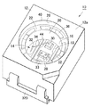
図1A〜図1Cに示した本実施の形態の発光装置10は、開口部38が円形状で、断面が逆台形状の凹部14を備えたハウジング12と、凹部14の底部18に露出した複数のリード電極32とを備えている。リード電極32の上には、発光素子28と、発光素子28を電気的に保護するための保護素子30とがダイボンドされ、さらに導電ワイヤ34によってリード電極32と導通されている。発光素子28は、凹部14の底部18に露出したリード電極32に、導電ワイヤ34によりワイヤボンディングされて電気的に接続している。リード電極32は、ハウジング12を貫通して外部電極320と接続されているので、外部電極320に電圧をかけることにより発光素子28に給電することができる。
[Embodiment 1]
1A to 1C, the
凹部14の内壁面16と開口部内縁20との間には、凹部の開口方向から見て環状に連続した段差が存在しており、この段差が遮光部22となっている。本明細書で「開口部内縁20」とは、開口部38近傍の凹部14の内壁面16を意味しており、詳しくは、開口部38の角部40から、凹部14の底部18方向に向かって、凹部14の深さの約30%程度までの範囲の内壁面16を指している。なお、凹部14の深さは、発光面12aから凹部14の底部18までの距離であり、図1Cでは、第1領域R1の厚さと、第2領域R2の厚さとの合計に相当する。
遮光部22は、その頂部がハウジング12の発光面12aよりも低い位置になるように形成されている。この遮光部22は、開口部38の角部40直下の開口部内縁20が、発光素子28の発光に直接照射されることがないように配置されている。すなわち、遮光部22は、発光素子28の発光面の両端部と開口部38の角部40とをそれぞれ結んだ線L1〜L2の間を確実に遮るように形成されている。このような遮光状態を、本明細書では「完全遮光」と称する。これにより、発光素子28からの発光は、遮光部22に遮蔽されて、開口部内縁20に直接到達することはない。発光素子26からの直接光が開口部内縁20に照射されて、開口部内縁20と封止材料26との接着性が低下する、という問題は、この遮光部22によって解決することができる。
Between the
The
図示されている遮光部22は、開口部内縁20の完全遮光をするのに適した高さに形成されている。ここで、遮光部22の高さは、凹部14の底部18から、遮光部22の頂部までの距離とし、第1領域R1の厚さと一致するものである。
しかしながら、開口部内縁20は、完全に遮光されなくても、部分的に遮光(本発明では「部分遮光」と称する)されているだけでも、開口部内縁20と封止樹脂26との剥離を十分に抑制する効果がある。本発明の発光装置10の構成であれば、遮光部22の高さが、完全遮光に必要な遮光部22の高さ(第1領域R1の厚さに相当)の80%以上にされていれば、剥離の抑制に有効である。これは、開口部内縁22のうち、開口部38の角部40付近が封止樹脂26から僅かに剥離したとしても、それ以外の開口部内縁の領域の剥離が抑えられていれば、発光装置内への不純物などの侵入は抑制できるので、信頼性が高く長寿命の発光装置を得るという本発明の目的は達成できるからである。遮光部22の高さが、第1領域R1の厚さに対して80%未満であると、直接光に露光される開口内縁部20の領域が広くなりすぎて、封止樹脂26と開口部内縁20との剥離が顕著になり、不純物の侵入等が起こる可能性が高まるので好ましくない。
The
However, even if the opening
凹部14の内部には、透光性の封止材料が遮光部22を越えて充填されている。つまり、透光性の封止材料26は、遮光部22の最頂部よりも高い位置にあるハウジング12の発光面12aと略同一平面まで充填されている。この封止樹脂26は、発光素子28を外部環境から保護する機能がある。また、ハウジング12の凹部14内は、遮光部22の頂部よりも低い位置にある第1領域R1と、遮光部22の頂部よりも高い位置にある第2領域R2に区分される。
The
封止材料26には、封止材料の物性を調節するために種々の粒状添加物が添加されている。本発明で使用される粒状添加物には、例えば、発光素子28からの発光を吸収して異なる波長に変換するための蛍光体粒子や、発光素子28からの光を拡散するための粉末状拡散材や、粘度や熱膨張係数などの物性を調節するための粒子状酸化物などが含まれる。これらの材料は、1種類のみで、又は複数種類を同時に使用することができる。
Various particulate additives are added to the sealing
粒状添加物に使用される材料は光を散乱する性質を有している。そのため、粒状添加物が第1領域R1に多量に含まれると、粒状添加物が発光素子28からの直接光を散乱する。その結果、凹部14の内壁面16に照射される直接光が低減される。これにより、内壁面16が直接光を吸収して材料劣化するのを抑制できるという効果がある。その反面、粒状添加物が第2領域R2に大量に含まれても、開口内縁部20は遮光部22によって直接光から遮光されているので、散乱による材料劣化抑制の効果は得られない。逆に、散乱した光が遮光部22を越えて開口部内縁20に到達すれば、遮光部22によって完全遮光した領域に散乱光が照射されることになる。散乱光の強度は、直接照射される光の強度に比べれば弱いが、散乱される光が多くなれば、散乱光による開口部内縁20の劣化が無視できなくなる。
The material used for the particulate additive has the property of scattering light. Therefore, when a large amount of particulate additive is contained in the first region R 1 , the particulate additive scatters direct light from the
この問題に対して、本発明の第1の発光装置10では、遮光部22より下側の第1領域R1に充填されている封止材料26中の粒状添加物の添加量を、光を散乱するのに十分な量以上にすることにより、発光素子28からの直接光を散乱させて、発光素子26からハウジング12の凹部14の内壁面16に到達する直接光を減少させることができ、そして、遮光部22より上側の第2領域R2に充填されている封止材料26中の粒状添加物の添加量を、光の散乱に実質的に影響を及ぼさない量以下にすることにより、第2領域R2の封止材料26によって散乱された散乱光が、開口部内縁20に到達するのを抑制している。
In order to solve this problem, in the first
本発明の第2の発光装置10では、封止材料26に、凹部14の底部18側にあり粒状添加物を含有する第1封止層261があり、封止材料26の厚さT1+T2に対する第1封止層261の厚さT1の割合T1/(T1+T2)が、10%〜80%としている。この割合が10%未満であると、発光素子28の上面が第1封止層261から露出して、第1封止層261による発光素子光の十分な散乱効果が得られない。また、この割合が80%より大きいと、発光素子28の近傍にある粒状添加物の密度が低くなって、やはり散乱効果が低くなる。すなわち、第2の発光装置は、粒状添加物を含む第1封止層が発光素子28を完全に覆った状態で、且つ発光素子28の近傍に集中して存在させることができるので、発光素子28からの直接光の散乱効果を向上させることができるといえる。また、第1封止層261の上面が遮光部22の上端よりも下側にあることにより、発光素子28からの直接光が粒状添加物によって散乱されても、開口部内縁に到達することがない。
In the second
そして、第3の発光装置10では、封止材料26中における粒径2.0μm以上の粒状添加物の最大密度は、第2領域R2の方が第1領域R1よりも低く、第2領域R2の粒状添加物の最大密度が、第1領域R1の粒状添加物の最大密度の80%以下に設定されている。これにより、第1領域R1においては粒状添加物による散乱を高めて、発光素子からハウジング12の凹部14の内壁面16に到達する直接光を減少させることができると共に、第2領域R2においては散乱を抑えて開口部内縁20に散乱光が照射されるのを抑制している。
本明細書において、「粒径」とは平均粒径を指しており、空気透過法により比表面積を測定し、一次粒子の粒径の平均値を求めたものであり、フィッシャー・サブ・シーブ・サイザー(F.S.S.S,)を用いて測定した値である。
In the third
In this specification, “particle diameter” refers to an average particle diameter, a specific surface area is measured by an air permeation method, and an average value of particle diameters of primary particles is obtained. It is a value measured using a sizer (FSSS).
特に、多量に含有されて散乱に影響を与える可能性の高い蛍光体粒子について規定し、散乱に対する影響の大きい粒径2.0μm以上の蛍光体粒子が、最大密度で比較したときに、第1領域R1に比べて第2領域R2で低く、第2領域R2の粒状添加物の最大密度が、第1領域R1の蛍光体粒子の最大密度の50%以下であるのが好ましい。この割合が50%を越えると、散乱光の影響が無視できなくなるので好ましくない。 In particular, phosphor particles that are contained in a large amount and have a high possibility of affecting scattering are defined. When phosphor particles having a particle size of 2.0 μm or more having a large influence on scattering are compared at the maximum density, lower in the second region R 2 as compared to the region R 1, the maximum density of the granular additives in the second region R 2 is is preferably not more than 50% of the maximum density of the first region R 1 of the phosphor particles. If this ratio exceeds 50%, the influence of scattered light cannot be ignored, which is not preferable.
なお、本発明に適した別の発光装置10は、第2領域R2に充填された封止材料26中に含有される粒状添加物の密度によって規定することもできる。このときの粒状添加物の密度には、散乱への影響を反映する観点から、単位体積当たりに含有される粒子重量又は粒子個数で規定することができる。また、製造後に適切な密度を有しているか確認するのに適しているという観点から、発光素子を切断したときの封止樹脂の切断面における、単位面積当たりに存在する粒子の個数で規定することもできる。
また、粒状添加物のうちでも、特に、多量に含有されて散乱に影響を与える可能性の高い蛍光体粒子に着目して、その密度を制御することも好ましい。
Incidentally, another
In addition, among the granular additives, it is also preferable to pay attention to phosphor particles that are contained in a large amount and have a high possibility of affecting scattering, and to control the density thereof.
図1Cに示すように、本実施の形態の発光装置10では、封止材料26を、第1封止層261と第2封止層262とを順次積層した積層構造としている。第1封止層261は、粒状添加物を含有した透光性の封止材料から形成されており、凹部14の底部18側(発光素子28の近傍)に配置される。第2封止層262は、粒状添加物を含有しない、又は所定の量以下の粒状添加物を含む封止材料から形成されており、第1封止層261の上側(すなわち発光面12a側)に配置される。
As shown in FIG. 1C, in the
このような積層タイプの封止材料26は、第1封止層261を充填し、続いて第2封止層262を充填することにより形成するので、第1封止層261と第2封止層262とは、明確な境界線によって区分される。そのため、第1封止層261に高密度で粒状添加物を含有させても、第2封止層262に粒状添加物が滲み出すことがなく、第2封止層262の粒状添加物密度を正確に調節することができる。
Since such a laminated
また、上記積層タイプとは別の封止材料26として、一度の樹脂充填によって形成するものがある。すなわち、粒状添加物を混合した液状の封止材料を凹部14にポッティングして静置し、封止材料が硬化するまでの間に、粒状添加物が凹部14の開口38部から底部18方向に沈降して、第1封止層261と第2封止層262とを構成する。
一度の樹脂充填によって形成された封止材料は、上述のように二回の充填によって形成する場合に比べると、工程数が少なく、製造容易であるという利点がある。その反面、第1封止層261と第2封止層262との境界位置を正確に設定できないという欠点がある。この問題は、第1封止層261の厚さを規定するときに、特に問題になる。そこで、本発明では、第1封止層の境界を、以下のように規定する。
In addition, as a sealing
The sealing material formed by filling the resin once has an advantage that the number of steps is small and the manufacturing is easy as compared with the case of forming the resin by filling twice as described above. On the other hand, there is a disadvantage that the boundary position between the
一般的に、封止材料26に混入した粒状添加物は、ポッティング後に、下方に向かって等しく沈降するが、内壁面16に隣接した領域では、壁面16と封止樹脂26との摩擦によって、粒状添加物の沈降が妨げられる傾向が見られる。その結果、壁面近傍では、沈降しきれなかった粒状添加物が分布することがある。しかしながら、内壁面近傍に分布する粒状添加物の密度は低く、散乱に与える影響も低いと考えることができる。そこで、本発明では、主に、適切に沈降した粒状添加物について討論するものとし、上記摩擦の影響が最も少ないと考えられる、内壁面16から最も離れた部分、すなわち凹部14の中央付近における第1封止層261の境界位置を、本発明における「第1封止層の境界」と規定する。また、凹部14の中央付近に発光素子28が配置されていると、発光素子28に沿って第1封止層261が部分的に盛り上がることがある。このような場合には、「第1封止層の厚さ」は、凹部14の底面から、第1封止層261の盛り上がった頂部の位置までの厚さと見なすこととする。
Generally, the particulate additive mixed in the sealing
本実施の形態では、開口部内縁20と遮光部22との間に、溝部24が形成されている。この溝部24は、開口部内縁20から遮光部22までの間の表面積が増加するので、封止材料26とハウジング12の凹部14内面との接触面を増やすことができる。これにより、封止部材26がハウジング12の凹部14内に係止しやすくなり、封止部材26の脱落を防止する効果もある。
遮光部22は、図1Cに示されるような矩形の断面形状や、山形の断面形状など、さまざまな断面形状にすることができる。
いずれの形状の遮光部22であっても、封止材料26との接触面積を増加させることができるので、封止部材26が剥離しにくく信頼性の高い発光装置を得ることができる。
In the present embodiment, a
The
Even if it is the
本実施の形態のリード電極32のいくつかには、貫通孔33が厚さ方向に形成されている(例えば、図1Bに示されるハウジング12の凹部の底面にて露出されたリード電極のうち、右側、左側、及び下側のリード電極32)。貫通孔33からは、ハウジング12の底部18が露出している。リード電極32に貫通孔33を形成することは、凹部14に封止樹脂26を充填したときに、封止樹脂26がリード電極32と接触する面積が減り、ハウジング材料と接触する面積が増加することになる。封止材料26とハウジング材料との接着性は、封止樹脂26とリード電極32との接着性よりも高いので、ハウジング12と封止樹脂26との固定力を増加させることができる。
このようなハウジング材料―封止樹脂26間の接着部分が、例えば発光素子28の周囲に位置するように設計すると、発光素子28がリード電極32から剥離するのを抑制することができる。図1Bでは、発光素子28が固定されているリード電極32は、三方(右側、左側、及び上側)が、リード電極間の隙間部(ハウジング材料が露出している)であり、下側には貫通孔33が形成されている。このようにハウジング材料を露出させることにより、発光素子28がリード電極から剥離しにくくなる。
また、上述したハウジング材料―封止樹脂26間の接着部分は、発光素子28の周囲だけでなく、導電ワイヤ34のボンディングする位置の周辺にも配置させることもできる。このように、貫通孔33を、導電ワイヤ34のボンディングする位置の近傍に形成すると、導電ワイヤ34がリード電極32から剥離しにくくすることができる。
In some of the
If such a bonding portion between the housing material and the sealing
Further, the above-mentioned bonding portion between the housing material and the sealing
(第1変形例)
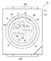
図2A及び図2Bは、本実施の形態の第1の変形例であり、リード電極32の形状と、発光素子28及び保護素子30の実装形態が異なっている。リード電極32の1つを長く形成することにより、発光素子28と保護素子30とを同一のリード電極32に実装することにより、発光素子28をハウジング12の凹部14の中央に実装することができ、これにより発光装置10の発光パターンを等方的にすることができる。
なお、このように発光素子28と保護素子30とを実装するリード電極32を変更する場合には、各素子の電極の極性及びリード電極の極性を考慮しなくてはならない。すなわち、素子の電極極性及びリード電極の極性を考慮すれば、発光素子28と保護素子30とは、様々な実装形態に変更可能である。
(First modification)
2A and 2B show a first modification of the present embodiment, in which the shape of the
In addition, when changing the
(第2変形例)
図3A及び3Bは、本実施の形態の第2変形例であり、遮光部22の外周に溝部24を設ける代わりに、遮光部22の上側に、複数の凸部36(この例では4つ)を、間隔をあけて形成している。また、各凸部36には、円周方向の中央付近に浅い溝(遮光部22よりも突出している)が形成されている。このような凸部は、溝部24と同様に表面積を増加させることができるので、封止材料26とハウジング12の凹部14内面との接触面を増やすことができる。これにより、封止部材26がハウジング12の凹部14内に係止しやすくなり、封止部材26の脱落を防止する効果がある。
さらに、封止材料26を充填するときには、凹部14内にポッティングされた封止材料26が、凸部36と凸部36との間を通って凸部36の外周側にも伝うので、空気の封入が起こりにくい。これにより、封止材料26中に泡が封入されて不良品となる発光装置10の発生を抑えることができる。
(Second modification)
3A and 3B show a second modification of the present embodiment. Instead of providing the
Furthermore, when the sealing
この第2変形例では、凹部14底部18のリードフレーム間にグリッド44(格子状の突出部)が形成されており、発光素子28や保護素子30をダイボンドするときの接着剤が、導電ワイヤ34をワイヤボンディングする位置まで広がることを防止している。このようなグリッド44は、ハウジング12と一体に形成されるのが好ましい。
In this second modification, a grid 44 (lattice-like protrusion) is formed between the lead frames of the
また、グリッド44は、リード電極32の表面を横断するように形成することもできる。グリッド44とリード電極32の表面との接着力が弱くなるような材料が選択されたとき、グリッド44はリード電極32から容易に剥がれてしまう。そこで、グリッド44の脱落を防止するために、グリッド44の一部を、ハウジング12の凹部14の底部18や内壁面16と接続することができる。また、グリッド44とリード電極32との接触面積を増加させて、接着力を高めることもできる。以下に、グリッド44の脱落防止用の形態を例示する。これらの例示は、1つだけで、又は複数を組み合わせて適用することができる。
(1)グリッド44を形成する位置に合わせて、リードフレーム32に貫通孔33を形成する。この貫通孔33を介して、グリッド44とハウジング12の底部18とを接続する。これにより、グリッド44が底部18に強固に固定され、それに伴ってリード電極32も底部18に固定される。
(2)グリッド44を凹部14の内壁面16まで延長して、グリッド44の端部と内壁面16とを接続させる。グリッド44の長さを長くすると、グリッド44が浮き上がりやすくなるので、グリッド44の両端を接続する内壁面16の2箇所の間隔が最大となる位置(例えば、上面円形の凹部14では、その直径に相当する位置)を避けて、グリッド44を形成することが好ましい。
(3)グリッド44を形成する位置に合わせて、リード電極32に溝を形成しておく。溝によってグリッド44とリード電極32との接触面積が増加し、グリッド44が脱落しにくくなる。
The
(1) The through
(2) The
(3) A groove is formed in the
以下に、本発明の発光装置10の各構成部材について詳述する。
(封止材料26)
ハウジングの凹部内には、透光性の封止材料が充填されており、発光素子、保護素子や導電ワイヤを外的環境から保護している。
封止部材26に適した透光性の封止材料としては、エポキシ樹脂、シリコーン樹脂、ユリア樹脂、フッ素樹脂、及びそれらの樹脂材料を複数混合した混合樹脂等の樹脂材料や、ガラス等の無機材料が挙げられる。特に、シリコーン樹脂は、透光性や耐熱性にすぐれているので、封止材料として利用するのに適している。シリコーン樹脂とハウジング12との接着力を向上させるため、本発明の発光装置10のように、遮光部22を備え且つ第2領域R2の粒状添加物密度を制限することにより、シリコーン樹脂と開口部内縁20との剥離を抑えることができる。すなわち、本発明の発光装置10は、封止部材26にシリコーン樹脂を使用することにより、従来よりも光の取出し効率が良く、比較的寿命の長い発光装置10を得ることができる。
Below, each structural member of the light-emitting
(Sealing material 26)
The concave portion of the housing is filled with a translucent sealing material to protect the light emitting element, the protective element, and the conductive wire from the external environment.
Examples of the light-transmitting sealing material suitable for the sealing
(粒状添加物)
本発明のような発光装置10に使用される主な粒状添加物としては、粉末状の蛍光体粒子、粉末状の拡散材、粒状の酸化物がある。
蛍光体粒子としては、以下の蛍光物質などが使用される。
(Granular additive)
The main particulate additives used in the
As the phosphor particles, the following fluorescent substances are used.
蛍光物質は、発光素子からの光を吸収し異なる波長の光に波長変換するものであればよい。例えば、Eu、Ce等のランタノイド系元素で主に賦活される窒化物系蛍光体・酸窒化物系蛍光体・サイアロン系蛍光体、Eu等のランタノイド系、Mn等の遷移金属系の元素により主に付活されるアルカリ土類ハロゲンアパタイト蛍光体、アルカリ土類金属ホウ酸ハロゲン蛍光体、アルカリ土類金属アルミン酸塩蛍光体、アルカリ土類ケイ酸塩蛍光体、アルカリ土類硫化物蛍光体、アルカリ土類チオガレート蛍光体、アルカリ土類窒化ケイ素蛍光体、ゲルマン酸塩蛍光体、又は、Ce等のランタノイド系元素で主に付活される希土類アルミン酸塩蛍光体、希土類ケイ酸塩蛍光体又はEu等のランタノイド系元素で主に賦活される有機及び有機錯体等から選ばれる少なくともいずれか1以上であることが好ましい。具体例として、下記の蛍光体を使用することができるが、これに限定されない。 The fluorescent substance may be any substance that absorbs light from the light emitting element and converts the wavelength into light of a different wavelength. For example, nitride phosphors / oxynitride phosphors / sialon phosphors mainly activated by lanthanoid elements such as Eu and Ce, lanthanoid elements such as Eu, and transition metal elements such as Mn. Activated alkaline earth halogen apatite phosphor, alkaline earth metal borate halogen phosphor, alkaline earth metal aluminate phosphor, alkaline earth silicate phosphor, alkaline earth sulfide phosphor, Alkaline earth thiogallate phosphor, alkaline earth silicon nitride phosphor, germanate phosphor, rare earth aluminate phosphor, rare earth silicate phosphor mainly activated with lanthanoid elements such as Ce It is preferably at least one selected from organic and organic complexes mainly activated by a lanthanoid element such as Eu. As specific examples, the following phosphors can be used, but are not limited thereto.
Eu、Ce等のランタノイド系元素で主に賦活される窒化物系蛍光体は、M2Si5N8:Eu、CaAlSiN3:Eu(Mは、Sr、Ca、Ba、Mg、Znから選ばれる少なくとも1種以上である。)などがある。また、M2Si5N8:EuのほかMSi7N10:Eu、M1.8Si5O0.2N8:Eu、M0.9Si7O0.1N10:Eu(Mは、Sr、Ca、Ba、Mg、Znから選ばれる少なくとも1種以上である。)などもある。
Eu、Ce等のランタノイド系元素で主に賦活される酸窒化物系蛍光体は、MSi2O2N2:Eu(Mは、Sr、Ca、Ba、Mg、Znから選ばれる少なくとも1種以上である。)などがある。
Eu、Ce等のランタノイド系元素で主に賦活されるサイアロン系蛍光体は、Mp/2Si12−p−qAlp+qOqN16−p:Ce、M−Al−Si−O−N(Mは、Sr、Ca、Ba、Mg、Znから選ばれる少なくとも1種以上である。qは0〜2.5、pは1.5〜3である。)などがある。
Eu等のランタノイド系、Mn等の遷移金属系の元素により主に付活されるアルカリ土類ハロゲンアパタイト蛍光体には、M5(PO4)3X:R(Mは、Sr、Ca、Ba、Mg、Znから選ばれる少なくとも1種以上である。Xは、F、Cl、Br、Iから選ばれる少なくとも1種以上である。Rは、Eu、Mn、EuとMn、のいずれか1以上である。)などがある。
Nitride-based phosphors mainly activated with lanthanoid elements such as Eu and Ce are M 2 Si 5 N 8 : Eu, CaAlSiN 3 : Eu (M is selected from Sr, Ca, Ba, Mg, Zn) At least one or more). In addition to M 2 Si 5 N 8 : Eu, MSi 7 N 10 : Eu, M 1.8 Si 5 O 0.2 N 8 : Eu, M 0.9 Si 7 O 0.1 N 10 : Eu (M Is at least one selected from Sr, Ca, Ba, Mg, and Zn.
An oxynitride phosphor mainly activated by a lanthanoid element such as Eu or Ce is MSi 2 O 2 N 2 : Eu (M is at least one selected from Sr, Ca, Ba, Mg, Zn) Etc.).
Eu, sialon phosphors activated mainly with lanthanoid elements such as Ce is, M p / 2 Si 12- p-q Al p + q O q N 16-p: Ce, M-Al-Si-O-N (M is at least one selected from Sr, Ca, Ba, Mg, and Zn. Q is 0 to 2.5, and p is 1.5 to 3).
Alkaline earth halogen apatite phosphors mainly activated by lanthanoid compounds such as Eu and transition metal elements such as Mn include M 5 (PO 4 ) 3 X: R (M is Sr, Ca, Ba). X is at least one selected from F, Cl, Br and I. R is any one of Eu, Mn, Eu and Mn. Etc.).
アルカリ土類金属ホウ酸ハロゲン蛍光体には、M2B5O9X:R(Mは、Sr、Ca、Ba、Mg、Znから選ばれる少なくとも1種以上である。Xは、F、Cl、Br、Iから選ばれる少なくとも1種以上である。Rは、Eu、Mn、EuとMn、のいずれか1以上である。)などがある。
アルカリ土類金属アルミン酸塩蛍光体には、SrAl2O4:R、Sr4Al14O25:R、CaAl2O4:R、BaMg2Al16O27:R、BaMg2Al16O12:R、BaMgAl10O17:R(Rは、Eu、Mn、EuとMn、のいずれか1以上である。)などがある。
アルカリ土類硫化物蛍光体には、La2O2S:Eu、Y2O2S:Eu、Gd2O2S:Euなどがある。
The alkaline earth metal borate phosphor has M 2 B 5 O 9 X: R (M is at least one selected from Sr, Ca, Ba, Mg, Zn. X is F, Cl , Br, or I. R is Eu, Mn, or any one of Eu and Mn.).
Alkaline earth metal aluminate phosphors include SrAl 2 O 4 : R, Sr 4 Al 14 O 25 : R, CaAl 2 O 4 : R, BaMg 2 Al 16 O 27 : R, BaMg 2 Al 16 O 12 : R, BaMgAl 10 O 17 : R (R is Eu, Mn, or any one of Eu and Mn).
Examples of the alkaline earth sulfide phosphor include La 2 O 2 S: Eu, Y 2 O 2 S: Eu, and Gd 2 O 2 S: Eu.
Ce等のランタノイド系元素で主に賦活される希土類アルミン酸塩蛍光体には、Y3Al5O12:Ce、(Y0.8Gd0.2)3Al5O12:Ce、Y3(Al0.8Ga0.2)5O12:Ce、(Y,Gd)3(Al,Ga)5O12の組成式で表されるYAG系蛍光体などがある。また、Yの一部若しくは全部をTb、Lu等で置換したTb3Al5O12:Ce、Lu3Al5O12:Ceなどもある。
その他の蛍光体には、ZnS:Eu、Zn2GeO4:Mn、MGa2S4:Eu(Mは、Sr、Ca、Ba、Mg、Znから選ばれる少なくとも1種以上である。Xは、F、Cl、Br、Iから選ばれる少なくとも1種以上である。)などがある。
Examples of rare earth aluminate phosphors mainly activated with lanthanoid elements such as Ce include Y 3 Al 5 O 12 : Ce, (Y 0.8 Gd 0.2 ) 3 Al 5 O 12 : Ce, Y 3 (Al 0.8 Ga 0.2) 5 O 12: Ce, and the like (Y, Gd) 3 (Al , Ga) YAG -based phosphor represented by the composition formula of 5 O 12. Further, there are Tb 3 Al 5 O 12 : Ce, Lu 3 Al 5 O 12 : Ce, etc. in which a part or all of Y is substituted with Tb, Lu or the like.
Other phosphors include ZnS: Eu, Zn 2 GeO 4 : Mn, MGa 2 S 4 : Eu (M is at least one selected from Sr, Ca, Ba, Mg, Zn. X is At least one selected from F, Cl, Br, and I).
上述の蛍光体は、所望に応じてEuに代えて、又は、Euに加えてTb、Cu、Ag、Au、Cr、Nd、Dy、Co、Ni、Tiから選択される1種以上を含有させることもできる。
また、上記蛍光体以外の蛍光体であって、同様の性能、効果を有する蛍光体も使用することができる。
The phosphor described above contains at least one selected from Tb, Cu, Ag, Au, Cr, Nd, Dy, Co, Ni, and Ti instead of Eu or in addition to Eu as desired. You can also
Moreover, it is fluorescent substance other than the said fluorescent substance, Comprising: The fluorescent substance which has the same performance and effect can also be used.
これらの蛍光体は、発光素子の励起光により、黄色、赤色、緑色、青色に発光スペクトルを有する蛍光体を使用することができるほか、これらの中間色である黄色、青緑色、橙色などに発光スペクトルを有する蛍光体も使用することができる。これらの蛍光体を種々組み合わせて使用することにより、種々の発光色を有する表面実装型発光装置を製造することができる。 These phosphors can use phosphors having emission spectra in yellow, red, green, and blue by the excitation light of the light-emitting element, and emission spectra in yellow, blue-green, orange, etc., which are intermediate colors between them. A phosphor having the following can also be used. By using these phosphors in various combinations, it is possible to manufacture surface-mounted light-emitting devices having various emission colors.
例えば、青色に発光するGaN系化合物半導体を用いて、Y3Al5O12:Ce若しくは(Y0.8Gd0.2)3Al5O12:Ceの蛍光物質に照射し、波長変換を行う。発光素子からの光と、蛍光体からの光との混合色により白色に発光する発光装置を提供することができる。 For example, using a GaN-based compound semiconductor that emits blue light, a Y 3 Al 5 O 12 : Ce or (Y 0.8 Gd 0.2 ) 3 Al 5 O 12 : Ce fluorescent material is irradiated to convert the wavelength. Do. A light emitting device that emits white light by a mixed color of light from a light emitting element and light from a phosphor can be provided.
例えば、緑色から黄色に発光するCaSi2O2N2:Eu又はSrSi2O2N2:Euと、蛍光体である青色に発光する(Sr,Ca)5(PO4)3Cl:Eu、赤色に発光するCa2Si5N8:Eu又はCaAlSiN3:Euと、からなる蛍光体を使用することによって、演色性の良好な白色に発光する発光装置を提供することができる。これは、色の三源色である赤・青・緑を使用しているため、第1の蛍光体及び第2の蛍光体の配合比を変えることのみで、所望の白色光を実現することができる。
特に、白色系の光を発する発光装置10では、青色発光の発光素子28に、アルミニウムを構成元素として含み、セリウムなどの希土類元素で付活されたアルミニウム酸化物系蛍光体(YAG:Ce)など青色光を吸収して黄色に発光する蛍光体が組み合わせて使用できる。以下、アルミニウム酸化物系蛍光体の一種であるイットリウム・アルミニウム・ガーネット系蛍光体の形成方法を説明する。まず、Y、Gd、Ceの希土類元素を化学量論比で酸に溶解した溶解液を蓚酸で共沈させる。これを焼成して得られる共沈酸化物と、酸化アルミニウムと混合して混合原料を得る。これにフラックスとしてフッ化アンモニウムを混合して坩堝に詰め、空気中1400℃の温度で3時間焼成して焼成品を得た。焼成品を水中でボールミルして、洗浄、分離、乾燥、最後に篩を通して形成させた。このようにして、Gd0.6Ce0.03Y2.4Al5O12で表される蛍光体を形成させる。
For example, CaSi 2 O 2 N 2 : Eu or SrSi 2 O 2 N 2 : Eu that emits light from green to yellow, and (Sr, Ca) 5 (PO 4 ) 3 Cl: Eu that emits blue light as a phosphor. By using a phosphor made of Ca 2 Si 5 N 8 : Eu or CaAlSiN 3 : Eu that emits red light, a light-emitting device that emits white light with good color rendering can be provided. This uses the three primary colors of red, blue, and green, so the desired white light can be achieved simply by changing the blend ratio of the first phosphor and the second phosphor. Can do.
In particular, in the
拡散材としては、シリカ、アルミナ、二酸化チタンなどが好適に利用でき、発光素子28からの光を拡散して、発光装置10の発光パターンをより均一にすることができる。
As the diffusing material, silica, alumina, titanium dioxide, or the like can be suitably used, and the light emitted from the
本形態における粒状酸化物としては、シリカ、アルミナ、ガラスが適している。これらの酸化物は、封止材料26の線膨張係数を低減して封止材料26に働く熱応力を低減する効果や、封止材料26の機械的強度を向上する効果がある。そのため、封止材料26の耐クラックが向上し、発光装置の寿命が長くなる。
As the granular oxide in this embodiment, silica, alumina, and glass are suitable. These oxides have the effect of reducing the thermal expansion acting on the sealing
(ハウジング12)
ハウジング12に適した材料としては、例えば、液晶ポリマー、ポリフタルアミド樹脂、ポリブチレンテレフタレート(PBT)などの熱可塑性樹脂を用いることができる。特に、ポリフタルアミド樹脂のような高融点結晶を含有する半結晶性ポリマー樹脂は、表面エネルギーが大きく、ハウジング12の凹部14に充填する封止樹脂との密着性が良好であるので、好適である。これにより、封止樹脂を充填し硬化する工程において、樹脂の冷却過程の間にハウジングと封止樹脂との界面が剥離しにくくなる。
また、ハウジング12の凹部14内壁面16は、発光素子28からの光を反射する反射板としても機能するので、凹部14の底部18に対する内壁面16の角度を調節して、発光装置10の発光効率を向上させるのが好ましい。このとき、発光素子28が半導体発光素子である半導体発光装置10を製造するならば、ハウジング12の成形材料中に酸化チタンなどの白色顔料などを混合して、内壁面16の反射率を高めて、反射効果を高めることもできる。
(Housing 12)
As a material suitable for the
Further, since the
(発光素子28)
発光素子28としては、半導体発光素子が好適に使用される。例えば、白色系の光を発する発光装置10を製造する場合には、窒化物半導体を使用した青色発光の発光素子28を使用することができる。上述のように、このような発光素子28を黄色発光する蛍光体と組み合わせることにより、白色光を発する発光装置10を得ることができる。
サファイア等の絶縁性基板を用いた窒化物半導体発光素子28は、導電ワイヤ34を用いたワイヤボンディングによって、リード電極32と導通されている。
(Light emitting element 28)
As the
The nitride semiconductor
(保護素子30)
保護素子30は、発光素子と並列接続して、発光素子を電気的に保護する素子であり、ツェナーダイオードなどが使用される。発光ダイオードのような発光素子10は、静電耐圧が低く、特に逆方向にサージ等の高電圧が印可されると静電破壊してしまう。この保護素子30を組み込むことにより、発光素子28に逆方向電流が印可された場合に、電流が保護素子30に流れるので、発光素子28が破壊させるのを回避できる。
保護素子30とリード電極32とは、裏面側(負極)を銀ペースト等の導電性ペーストで固定しながら、また表面側(正極)を導電ワイヤ34によるワイヤボンディングにより、それぞれ導通されている。
(Protective element 30)
The
The
(リード電極32/外部電極320)
リード電極32及び外部電極320は、すべて同一の導電性材料から形成されており、加工性や強度の観点からすると、鉄、銅、鉄入り銅、錫入り銅及び銅、金、銀をメッキしたアルミニウム、鉄、銅等から形成するのが好ましい。
(Lead
The
(導電ワイヤ34)
ワイヤボンディング用の導電ワイヤ34としては、例えば、金線、銅線、白金線、アルミニウム線等の金属及びそれらの合金から成る金属製のワイヤを用いることができる。導電ワイヤ34は、一端を素子(発光素子28や保護素子30)の電極に接合され、他端をリード電極32に接合されるが、特に他端の接合では、同じリード電極32に位置をずらして複数回接合するのが好ましい。例えば、図1Aの発光装置10では、リード電極32に接合された導電ワイヤ34の他端は、リード電極32上に2回ボンディングされている。このような複数回のボンディングを行うと、導電ワイヤ34とリード電極32との剥離が起こりにくくなり、導電ワイヤ34とリード電極32との間の電気的接続不良による発光装置10の不灯が発生しにくくなる。
(Conductive wire 34)
As the
本発明は、発光素子28からの直接光を遮光部22により遮光し、また遮光部22を越えて到達する散乱光を抑制することにより、開口部内縁20の劣化を抑制し、従来に比べて開口部内縁20と封止樹脂26との剥離を効果的に抑制する。これにより、寿命が長く信頼性の高い発光装置10を得ることができる。また、本発明により、従来では寿命短縮の原因となっていたシリコーン樹脂を、封止樹脂26として好適に使用することが可能になった。
In the present invention, the direct light from the
[実施の形態2]
実施の形態2は、図4及び図5に示すように、ハウジング12の凹部14の一部に切欠き部42を設けて、リード電極32の露出面積を広くした発光装置10である。切欠き部42から露出したリード電極32の上には、保護素子30がダイボンドされている。本実施の形態の発光装置10は、切欠き部42と保護素子30の実装位置を除いて、実施の形態1と同様である。
[Embodiment 2]
As shown in FIGS. 4 and 5, the second embodiment is a light emitting
本実施の形態のように切欠き部42を設けると、遮光部22が部分的に除去されることになる。よって、発光素子10からの直接光が、切欠き部42を通ってハウジング12の凹部14の開口部内縁20に照射されることになる。
しかしながら、切欠き部42を設けることにより、小型化された発光装置において保護素子30の実装が容易になる。また、発光装置の小型化により、凹部底面の中央における半導体素子の実装スペースが制限されても、発光素子以外の半導体素子や、その保護素子に接続するワイヤを切欠き部42内に配置することにより、発光素子28を凹部14の中央に配置することが可能になる。そして、切欠き部42の大きさは、そこに配置される半導体素子の大きさに対応させて必要最小限の大きさとされる。したがって、そこに充填される封止樹脂26の量も比較的少ないので、これにより封止材料26と凹部14の開口部内縁20との間に生じる膨張量の差が減少し、封止材料26と開口部内縁20との間の剥離が生じにくい。さらに、内部に充填する封止材料26の量を減らすことができるので、発光素子28や導電ワイヤ34に働く熱ストレスが小さくなり、発光装置10の信頼性が高まる効果も期待できる。
When the
However, the provision of the
このように、ハウジング12の凹部14に切欠き部42を設けることは、発光素子28から開口部内縁20に直接光が照射されるという欠点と同時に、発光素子28の実装位置の改善、開口部内縁20における封止樹脂26の剥離を抑制する効果や、発光装置10の信頼性向上などの有利な効果を奏する。よって、切欠き部42を設ける場合には、これらの欠点と利点とのバランスを取ることが望ましい。
特にバランスのよい切欠き部42の割合は、遮光部22の外周に沿った長さに基づいて定めるのが適切である。切欠き部42は、保護素子30を実装しやすいように、ほぼ平行に遮光部22を切除して形成され、このような切欠き部42を通過した直接光に露光される開口部内縁20の割合は、遮光部22の外周に依存するからである。
As described above, the provision of the
In particular, it is appropriate to determine the proportion of the well-
遮光部22の外周に沿って測定したとき、切欠き部42の長さをC、残存している遮光部22の長さをDとすると、切欠き部42を形成しなかった場合の遮光部22の長さ(C+D)に対する切欠き部42の割合C/(C+D)が、50%以下の範囲になるように、切欠き部42を形成するのが好ましい。切欠き部42の割合が50%より多くなると、直接光を遮光できないことによる剥離の問題が顕著になるので好ましくない。
When measuring along the outer periphery of the
切欠き部42には遮光部22が形成されていないので、封止材料26を充填するときには、凹部14内にポッティングされた封止材料26が切欠き部42から溝部24に流れ込むので、空気の封入が起こりにくい。これにより、封止材料36中に泡が封入されて発光装置10が不良になる、という問題を抑えることができる。
Since the
(第1変形例)
図6、図7A及び図7Bは、本実施の形態の第1の変形例であり、切欠き部42が2つ形成され、遮光部22が2つに分離している点で異なっている。切欠き部42を備えた発光装置10では、切欠き部42方向の光だけが広角に広がりやすく、発光パターンの外形が、部分的に飛び出した形状になる。この変形例は、切欠き部42を対向して形成することにより、切欠き部42が1つの形態に比べて、発光パターンを改善することができる。
これらの例では、切欠き部42の長さC=C1+C2、残存している遮光部22の長さD=D1+D2として、切欠き部42の割合C/(C+D)を算出することができる。
(First modification)
FIG. 6, FIG. 7A and FIG. 7B show a first modification of the present embodiment, which is different in that two
In these examples, the ratio C / (C + D) of the
また、図7A及び図7Bの発光装置10では、凹部14底部18のリードフレーム間にグリッド44が形成されており、発光素子28や保護素子をダイボンドするときの接着剤が、導電ワイヤ34に接触するのを防止している。さらに、切欠き部42の内側に、凹部14の深さ方向に延びたリッジ46を形成しており、肉薄になっている切欠き部42を補強して、ハウジング12全体の強度を高めている。グリッド44やリッジ46は、ハウジング12と一体に形成されるのが好ましい。
Further, in the
(第2変形例)
図8は、本実施の形態の第2の変形例であり、切欠き部42が4つ形成され、遮光部22が4つに分離している。この変形例は、4つの切欠き部42を均等に配置することにより、切欠き部42が1つ又は2つの形態に比べて、発光パターンをより改善することができる。
この変形例では、切欠き部42の長さC=C1+C2+C3+C4、残存している遮光部22の長さD=D1+D2+D3+D4として、切欠き部42の割合C/(C+D)を算出することができる。
(Second modification)
FIG. 8 shows a second modification of the present embodiment, in which four
In this modification, the length C of the
また、凹部14底部18のリードフレーム間にグリッド44が形成されており、発光素子28や保護素子をダイボンドするときの接着剤が、導電ワイヤ34に接触するのを防止している。グリッド44は、ハウジング12と一体に形成されるのが好ましい。
Further, a
[実施の形態3]
図9A〜図9Dに示す実施の形態3の発光装置10は、実施の形態1及び2で説明した上面発光型発光装置とは異なり、薄型の液晶のバックライトに適した側面発光型発光装置である。そのため、ハウジング12、リード電極32の形状が異なっており、また保護素子30を実装しない形態をとっているが、それらを除いて、実施の形態1及び2と同様である。
[Embodiment 3]
A
扁平形状のハウジング12は、発光面12aに開口した凹部14を備え、その凹部14の底部18には、部分的にリード電極32が露出している。リード電極32の上には、発光素子28がダイボンドされ、さらに導電ワイヤ34によってリード電極32と導通されている。リード電極32の表面には、発光素子28にダイボンド位置の両側に、2本のグリッド44が平行に形成されており、発光素子28やダイボンドするときの接着剤が、導電ワイヤ34をワイヤボンディングする位置まで広がることを防止している。
リード電極32は、ハウジング12を貫通して外部電極320まで伸びているので、外部電極320に電圧をかけることにより発光素子28に給電することができる。なお、この例では外部電極320はハウジング32の側壁から突出しているが、必要に応じて外部電極320を折り曲げてハウジング32に沿わせるようにすることができる。
The flat-shaped
Since the
凹部14の内壁面16と開口部内縁20との間には、遮光部22が形成されており、開口部38の開口部内縁20が、発光素子28の発光に直接照射されることがないように配置されている。遮光部22は、その頂部がハウジング12の発光面12aよりも低い位置になるように形成されている。本実施の形態では凹部14の開口部の形状が多角形(この図では6角形)になっているので、遮光部22は、その多角形の各辺に沿って直線状に形成されている。
A
凹部14の内部には、透光性の封止材料が遮光部22を越えて充填されている。つまり、透光性の封止材料26は、遮光部22の最頂部よりも高い位置にあるハウジング12の発光面12aと略同一平面まで充填されている。この封止樹脂26は、発光素子28を外部環境から保護する機能がある。また、ハウジング12の凹部14内は、遮光部22よりも低い位置にある第1領域R1と、遮光部22の頂部よりも高い位置にある第2領域R2に区分される。
The
本実施の形態のようにハウジング12の寸法が小さくされる場合には、遮光部22の背面にある溝部24への樹脂流れが悪くなり、封止樹脂26内に空気が封入されることがある。これを防止するには、遮光部22の一部を除去しておくのが効果的である。遮光部22を除去する位置は任意に設定できるが、例えば図9A及び9Cでは、発光素子26からの距離の離れた4つの隅部の遮光部22を除去してある。発光素子26からの距離が離れていると、直接光が到達するまでに散乱されて強度が小さくなりやすいので、開口部内縁20の材料劣化が起こりにくいので好ましい。
図9Cは、図9AのC−C線に沿った断面図であるが、このC−C線は、遮光部22を除去された2つの隅部を通っている。図9Cに示すように、遮光部22が除去された隅部の凹部内壁面には段差が形成されている。この段差の上面は、粗面化されているのが好ましく、ハウジング12と封止樹脂26との接着力を向上させることができる。段差上面を粗面化するには、例えばハウジング12の形成に用いる金型で、段差上面に相当する成形面を放電加工により粗面にする方法が採用できる。
When the size of the
FIG. 9C is a cross-sectional view taken along the line CC in FIG. 9A, and the line CC passes through two corners from which the
(試料の調整)
図1Aに示したハウジング12の凹部14に、蛍光体粒子を含有する封止樹脂26をポッティングして、蛍光体粒子の沈降の状態を観察した。
凹部14の寸法は、底部18の直径が1.7mm、遮光部22の頂部の内径が1.8mm、外径が2.1mm、頂部の幅が0.3mm、開口部内縁20の直径が2.4mm、ハウジング12の発光面12aからの深さが0.8mmである。
封止樹脂26には、シリコーン樹脂(比重:1.4、ヤング率:0.3〜4MPa、線膨張係数:200〜400(10 −6 /℃)、粘度:1000〜20000(mPa・s))を使用した。蛍光体粒子は、平均粒径5.0±0.7μmの(Y0.98Gd0.02)2.85Ce0.15Al5O12(比重4.6)を使用した。
(Sample adjustment)
A sealing
The dimensions of the
The sealing
まず、ハウジング12の底部18に発光素子28と保護素子30とをダイボンド及びワイヤボンドにより実装した。その後に、ハウジング12の凹部14に、蛍光体粒子を19重量%の割合で混合したシリコーン樹脂を、充填した。その状態で静置して、シリコーン樹脂をおよそ17時間かけて硬化させた。
First, the
(試料の観察)
得られた試料を、凹部14の中央を通る面で切断して、切断面を金属顕微鏡(OLYMPUS社製、MODEL BX60)により観察した。観察時の条件は、倍率5倍で、フィルターを用いて明視野とした。本実施例の断面写真を図11に示す。
(Sample observation)
The obtained sample was cut along a plane passing through the center of the
(観察結果)
図10では、蛍光体粒子は黄色い粒状物質として確認することができる。図10から、以下のことが確認できる。
多くの蛍光体粒子が凹部14の底面に沈降して、凹部14の底面18、発光素子28及び保護素子30の上面に、高密度な蛍光体粒子層が形成されている(図中の破線で示す)。この蛍光体粒子層が、本発明の第1の発光装置10における第1封止層261に相当する。フィルター等の使用や光の照射方法を変更すると、さらに第1封止層261の界面を視認しやすくなる。
(Observation results)
In FIG. 10, the phosphor particles can be confirmed as a yellow granular material. From FIG. 10, the following can be confirmed.
Many phosphor particles settle on the bottom surface of the
また、蛍光体粒子層の厚さはほぼ均一であるが、発光素子28及び保護素子30が実装されている部分では、第1封止層261が部分的に盛り上がっている。このように部分的に盛り上がった形態では、本発明で規定した「第1封止層261の厚さ」は、底部18から、最も盛り上がった第1封止樹脂層261の頂部(この例では、図中右側の保護素子30の上に形成された第1封止樹脂層261)までの距離となる。本発明の第1封止層261の厚さは、封止樹脂26の厚さの30%程度であると見積もることができる。
Further, although the thickness of the phosphor particle layer is substantially uniform, the
遮光部22の外側に形成された溝部24の内側にも、蛍光体粒子が堆積していることが確認される。しかしながら、溝部24には発光素子28からの直接光が到達しないので、溝部24内の蛍光体粒子が、本発明において問題となる光の散乱には影響を与えない。
It is confirmed that the phosphor particles are also deposited inside the
なお、後述の実施例2と比較すると、本実施例の試料は、凹部14の内壁面16に蛍光体粒子がほとんど付着していない。本実施例のハウジング12では、凹部14の内壁面16が底面18に対してほぼ垂直であるため、蛍光体粒子を含む封止樹脂28が円滑に底面18方向に充填され、蛍光体粒子が底面18側に沈降したためであると考えられる。
In addition, compared with Example 2 described later, in the sample of this example, the phosphor particles are hardly attached to the
このように、封止樹脂26を1段階で形成した場合に、本発明の発光装置に適した粒状添加物の分布状態を実現できることが明らかになった。
As described above, it has been clarified that when the sealing
(試料の調製及び観察)
図9Aに示したハウジング12の凹部14に、蛍光体粒子を含有する封止樹脂26をポッティングして、蛍光体粒子の沈降の状態を観察した。
凹部14は、発光面12a方向から観察して細長い形状をしており、凹部の開口部の幅は、発光面12の中央から両端に向かって小さくなっており、中央付近で最大幅になっている。つまり、発光面12a方向から観察して、開口部の両端から、それぞれ、開口部の長手方向の幅1/3ほどの位置まで、発光面が大きくなるように、凹部14の内壁面16の一方が他方に向かって傾斜しており、両端が最も狭幅になっている。
凹部14の底部18の寸法は、長さが2.5mm、最大幅が0.65mm、最小幅が0.4mmであり、ハウジング12の発光面12aから底面18までの深さが0.6mmである。また、凹部14の内壁面16は、底部18から開口部38に向かって凹部の内径が徐々に広がるように、全体が僅かに傾斜している。また、凹部の内壁面に形成された遮光部22は、幅が0.1mm、高さが0.08mmである。
(Sample preparation and observation)
A sealing
The
The dimensions of the bottom 18 of the
本実施例では、発光素子28と保護素子30とを実装せずに試料を調製した。シリコーン樹脂及び蛍光体粉末は、実施例1と同じものを使用した。ハウジングの凹部14に、蛍光体粒子を19重量%の割合で混合したシリコーン樹脂を充填し、その状態で静置して、シリコーン樹脂をおよそ17時間かけて硬化させた。
得られた試料は、図9AのD−D断面で切断して、実施例1と同様に観察した。本実施例の断面写真を図11に示す。
In this example, a sample was prepared without mounting the
The obtained sample was cut in the DD section of FIG. 9A and observed in the same manner as in Example 1. A cross-sectional photograph of this example is shown in FIG.
図11では、蛍光体粒子は黄色い粒状物質として確認することができる。図11から、以下のことが確認できる。
(1)多くの蛍光体粒子が凹部14の底面に沈降して、底面に高密度な蛍光体粒子層が形成されている。この蛍光体粒子層が、本発明の第1の発光装置10における第1封止層261に相当する。
(2)凹部14の内壁面16にも蛍光体粒子が付着している。これは、蛍光体粒子が沈降している間に内壁面16と接触すると、内壁面16との摩擦によって沈降速度が遅くなったため、封止樹脂26の硬化が完了するまでに沈降しきらなかったものであると考えられる。その結果、内壁面16近傍の蛍光体粒子層が、凹部の底面から内壁面に沿って這い上がったような状態が観察される。
(3)遮光部22の外側に形成された溝部24の内側にも、蛍光体粒子が堆積している。
In FIG. 11, the phosphor particles can be confirmed as a yellow granular material. From FIG. 11, the following can be confirmed.
(1) Many phosphor particles settle on the bottom surface of the
(2) The phosphor particles are also attached to the
(3) The phosphor particles are also deposited inside the
図11の写真から、凹部14の中央付近に存在する蛍光体粒子は、上記(1)の第1封止層261のみであった。また、第1封止層261の界面は、視認によって明確に規定できることもわかった。
上記(2)の内壁面近傍の蛍光体粒子の密度は、それほど高くないので、光の散乱に対して十分な効果を与えるとは考えにくい。
上記(3)の溝部24に堆積した蛍光体粒子は、溝部24に直接光が到達しないので、本発明において問題となる光の散乱には影響を与えない。
From the photograph of FIG. 11, the phosphor particles present in the vicinity of the center of the
Since the density of the phosphor particles in the vicinity of the inner wall surface in (2) is not so high, it is unlikely that the phosphor particles have a sufficient effect on light scattering.
The phosphor particles deposited in the groove part (3) do not directly reach the
このように、封止樹脂26を1段階で形成した場合に、本発明の発光装置に適した粒状添加物の分布状態を実現できることが明らかになった。
As described above, it has been clarified that when the sealing
本発明の発光装置は、自動車用前照灯や車内光源のように、高出力かつ高信頼性が必要な発光装置に利用可能である。 The light-emitting device of the present invention can be used for a light-emitting device that requires high output and high reliability, such as an automotive headlamp or an in-vehicle light source.
10 発光装置、 12 ハウジング、 12a 発光面、 14 凹部、 16 凹部の内壁面、 18 凹部の底部、 20 開口部内縁、 22 遮光部、 24 溝部、 26 透光性の封止材料、 261 第1封止層、 262 第2封止層、 28 発光素子、 30 保護素子、 32 リード電極、 320 外部電極、 34 導電ワイヤ、 36 凸部、 38 開口部、 40 開口部の角部、 42 切欠き部、
R1 第1領域、 R2 第2領域、 T1 第1封止層の厚さ、 T2 第2封止層の厚さ。
DESCRIPTION OF
R 1 first region, R 2 second region, T 1 thickness of first sealing layer, T 2 thickness of second sealing layer.
Claims (7)
前記発光素子を収納する凹部を備えたハウジングと、
前記凹部の底部に露出した第1リード電極及び第2リード電極と、
前記発光素子の一対の電極と、前記第1リード電極及び前記第2リード電極とをそれぞれ電気的に接続する導電部材と、
前記凹部に充填された透光性の封止材料と、
前記封止材料に含有され、前記発光素子の発光を吸収して異なる波長に変換する蛍光体粒子を含む粒状添加物と、を備えた発光装置であって、
前記凹部の内壁面は、前記発光素子から前記凹部の開口部内縁に照射される光を遮光する遮光部を備えており、
前記封止材料中の前記粒状添加物の添加量は、前記遮光部より下側の第1領域では、光の散乱を高める量に調整されており、かつ、前記遮光部より上側の第2領域では、光の散乱を抑制する量に調整されていることを特徴とする発光装置。 A light emitting device having a pair of electrodes;
A housing having a recess for housing the light emitting element;
A first lead electrode and a second lead electrode exposed at the bottom of the recess;
A conductive member that electrically connects the pair of electrodes of the light emitting element to the first lead electrode and the second lead electrode;
A light-transmitting sealing material filled in the recess;
A granular additive containing phosphor particles that are contained in the sealing material and absorb light emitted from the light emitting element and convert the light into different wavelengths , and a light emitting device comprising:
The inner wall surface of the concave portion includes a light shielding portion that shields light emitted from the light emitting element to the inner edge of the opening of the concave portion,
The addition amount of the particulate additive in the sealing material is adjusted to an amount that increases light scattering in the first region below the light shielding portion, and the second region above the light shielding portion. Then, the light-emitting device adjusted to the quantity which suppresses scattering of light.
前記発光素子を収納する凹部を備えたハウジングと、
前記凹部の底部に露出した第1リード電極及び第2リード電極と、
前記発光素子の一対の電極と、前記第1リード電極及び前記第2リード電極とをそれぞれ電気的に接続する導電部材と、
前記凹部に充填された透光性の封止材料と、
前記封止材料に含有され、前記発光素子の発光を吸収して異なる波長に変換する蛍光体粒子を含む粒状添加物と、を備えた発光装置であって、
前記凹部の内壁面は、前記発光素子から前記凹部の開口部内縁に照射される光を遮光する遮光部を備えており、
前記封止材料の前記凹部の底部側は、前記粒状添加物を含有する第1封止層であり、
前記第1封止層の厚さが前記封止材料の厚さの10%〜80%で、且つ前記第1封止層の上面が前記遮光部の上端よりも下側にあることを特徴とする発光装置。 A light emitting device having a pair of electrodes;
A housing having a recess for housing the light emitting element;
A first lead electrode and a second lead electrode exposed at the bottom of the recess;
A conductive member that electrically connects the pair of electrodes of the light emitting element to the first lead electrode and the second lead electrode;
A light-transmitting sealing material filled in the recess;
A granular additive containing phosphor particles that are contained in the sealing material and absorb light emitted from the light emitting element and convert the light into different wavelengths , and a light emitting device comprising:
The inner wall surface of the concave portion includes a light shielding portion that shields light emitted from the light emitting element to the inner edge of the opening of the concave portion,
The bottom side of the recess of the sealing material is a first sealing layer containing the particulate additive,
The thickness of the first sealing layer is 10% to 80% of the thickness of the sealing material, and the upper surface of the first sealing layer is below the upper end of the light shielding part. Light-emitting device.
前記発光素子を収納する凹部を備えたハウジングと、
前記凹部の底部に露出した第1リード電極及び第2リード電極と、
前記発光素子の一対の電極と、前記第1リード電極及び前記第2リード電極とをそれぞれ電気的に接続する導電部材と、
前記凹部に充填された透光性の封止材料と、
前記封止材料に含有され、前記発光素子の発光を吸収して異なる波長に変換する蛍光体粒子を含む粒状添加物と、を備えた発光装置であって、
前記凹部の内壁面は、前記発光素子から前記凹部の開口部内縁に照射される光を遮光する遮光部を備えており、
前記封止材料中における粒径2.0μm以上の前記粒状添加物の最大密度が、前記遮光部より下側の第1領域に比べて、前記遮光部より上側の第2領域で低く、
前記第2領域の前記粒状添加物の前記最大密度が、前記第1領域の前記粒状添加物の前記最大密度の80%以下であることを特徴とする発光装置。 A light emitting device having a pair of electrodes;
A housing having a recess for housing the light emitting element;
A first lead electrode and a second lead electrode exposed at the bottom of the recess;
A conductive member that electrically connects the pair of electrodes of the light emitting element to the first lead electrode and the second lead electrode;
A light-transmitting sealing material filled in the recess;
A granular additive containing phosphor particles that are contained in the sealing material and absorb light emitted from the light emitting element and convert the light into different wavelengths , and a light emitting device comprising:
The inner wall surface of the concave portion includes a light shielding portion that shields light emitted from the light emitting element to the inner edge of the opening of the concave portion,
The maximum density of the granular additive having a particle size of 2.0 μm or more in the sealing material is lower in the second region above the light shielding part than in the first region below the light shielding part,
The light emitting device, wherein the maximum density of the granular additive in the second region is 80% or less of the maximum density of the granular additive in the first region.
Priority Applications (2)
| Application Number | Priority Date | Filing Date | Title |
|---|---|---|---|
| JP2006213929A JP5205724B2 (en) | 2006-08-04 | 2006-08-04 | Light emitting device |
| US11/882,603 US7815343B2 (en) | 2006-08-04 | 2007-08-02 | Light emitting device |
Applications Claiming Priority (1)
| Application Number | Priority Date | Filing Date | Title |
|---|---|---|---|
| JP2006213929A JP5205724B2 (en) | 2006-08-04 | 2006-08-04 | Light emitting device |
Related Child Applications (1)
| Application Number | Title | Priority Date | Filing Date |
|---|---|---|---|
| JP2012110401A Division JP5327356B2 (en) | 2012-05-14 | 2012-05-14 | Light emitting device |
Publications (3)
| Publication Number | Publication Date |
|---|---|
| JP2008041917A JP2008041917A (en) | 2008-02-21 |
| JP2008041917A5 JP2008041917A5 (en) | 2009-09-03 |
| JP5205724B2 true JP5205724B2 (en) | 2013-06-05 |
Family
ID=39050542
Family Applications (1)
| Application Number | Title | Priority Date | Filing Date |
|---|---|---|---|
| JP2006213929A Active JP5205724B2 (en) | 2006-08-04 | 2006-08-04 | Light emitting device |
Country Status (2)
| Country | Link |
|---|---|
| US (1) | US7815343B2 (en) |
| JP (1) | JP5205724B2 (en) |
Families Citing this family (72)
| Publication number | Priority date | Publication date | Assignee | Title |
|---|---|---|---|---|
| JP4783718B2 (en) * | 2006-11-27 | 2011-09-28 | 新光電気工業株式会社 | Lighting device |
| US7652297B2 (en) * | 2007-09-11 | 2010-01-26 | Avago Technologies Ecbu Ip (Singapore) Pte. Ltd. | Light emitting device |
| CN101493216B (en) * | 2008-01-24 | 2011-11-09 | 富士迈半导体精密工业(上海)有限公司 | LED light source module |
| JP5358104B2 (en) * | 2008-02-25 | 2013-12-04 | 豊田合成株式会社 | Light emitting device |
| JP5236406B2 (en) * | 2008-03-28 | 2013-07-17 | ローム株式会社 | Semiconductor light emitting module and manufacturing method thereof |
| KR101526567B1 (en) * | 2008-05-07 | 2015-06-10 | 엘지이노텍 주식회사 | Lighting emitting diode package |
| JP2010020962A (en) * | 2008-07-09 | 2010-01-28 | Kanehirodenshi Corp | Led lamp |
| US8022626B2 (en) * | 2008-09-16 | 2011-09-20 | Osram Sylvania Inc. | Lighting module |
| US8183585B2 (en) * | 2008-09-16 | 2012-05-22 | Osram Sylvania Inc. | Lighting module |
| US8188486B2 (en) * | 2008-09-16 | 2012-05-29 | Osram Sylvania Inc. | Optical disk for lighting module |
| US20100067240A1 (en) * | 2008-09-16 | 2010-03-18 | John Selverian | Optical Cup For Lighting Module |
| DE102009012517A1 (en) * | 2009-03-10 | 2010-09-16 | Osram Opto Semiconductors Gmbh | Optoelectronic semiconductor component |
| US8610156B2 (en) | 2009-03-10 | 2013-12-17 | Lg Innotek Co., Ltd. | Light emitting device package |
| KR101047603B1 (en) * | 2009-03-10 | 2011-07-07 | 엘지이노텍 주식회사 | Light emitting device package and its manufacturing method |
| CN102484211B (en) * | 2009-05-27 | 2015-01-28 | 皇家飞利浦电子股份有限公司 | Sealed thin-film device, method of and system for repairing sealing layer applied to thin-film device |
| TWI370216B (en) * | 2009-06-29 | 2012-08-11 | Lextar Electronics Corp | Led lighting device |
| JPWO2011037185A1 (en) * | 2009-09-24 | 2013-02-21 | 京セラ株式会社 | Mounting substrate, light emitter, and manufacturing method of mounting substrate |
| KR20110039080A (en) * | 2009-10-09 | 2011-04-15 | 알티반도체 주식회사 | Backlight unit and method for manufacturing thereof |
| CN102044600A (en) * | 2009-10-15 | 2011-05-04 | 展晶科技(深圳)有限公司 | Light-emitting diode (LED) encapsulating structure and preparation method thereof |
| USD661262S1 (en) * | 2009-10-26 | 2012-06-05 | Nichia Corporation | Light emitting diode |
| JP5311674B2 (en) * | 2010-01-14 | 2013-10-09 | パナソニック株式会社 | Light emitting device |
| KR101121151B1 (en) * | 2010-03-19 | 2012-03-20 | 주식회사 대원이노스트 | Led module and fabrication method of thereof |
| US8525213B2 (en) * | 2010-03-30 | 2013-09-03 | Lg Innotek Co., Ltd. | Light emitting device having multiple cavities and light unit having the same |
| WO2011126135A1 (en) | 2010-04-09 | 2011-10-13 | ローム株式会社 | Led module |
| KR101298406B1 (en) * | 2010-05-17 | 2013-08-20 | 엘지이노텍 주식회사 | Light Emitting Device |
| KR101039994B1 (en) * | 2010-05-24 | 2011-06-09 | 엘지이노텍 주식회사 | Light emitting device and light unit having thereof |
| TWI449866B (en) * | 2010-09-30 | 2014-08-21 | Hon Hai Prec Ind Co Ltd | Led illuminating device |
| JP5570018B2 (en) * | 2010-10-23 | 2014-08-13 | シチズン電子株式会社 | LED module |
| US20120236529A1 (en) * | 2011-03-15 | 2012-09-20 | Avago Technologies Ecbu Ip(Singapore) Pte. Ltd. | Method And Apparatus For A Light Source |
| US9041046B2 (en) | 2011-03-15 | 2015-05-26 | Avago Technologies General Ip (Singapore) Pte. Ltd. | Method and apparatus for a light source |
| WO2012124587A1 (en) * | 2011-03-16 | 2012-09-20 | シャープ株式会社 | Wavelength conversion member, production method for same, light-emitting device, illumination device, and headlight |
| DE102011105010A1 (en) * | 2011-06-20 | 2012-12-20 | Osram Opto Semiconductors Gmbh | Optoelectronic semiconductor component and method for its production |
| JPWO2013011628A1 (en) * | 2011-07-19 | 2015-02-23 | パナソニック株式会社 | Light emitting device and manufacturing method thereof |
| US10211380B2 (en) * | 2011-07-21 | 2019-02-19 | Cree, Inc. | Light emitting devices and components having improved chemical resistance and related methods |
| US10686107B2 (en) * | 2011-07-21 | 2020-06-16 | Cree, Inc. | Light emitter devices and components with improved chemical resistance and related methods |
| CN103000782B (en) * | 2011-09-13 | 2016-09-07 | 展晶科技(深圳)有限公司 | Package structure for LED |
| CN104054189B (en) * | 2011-11-17 | 2018-06-26 | 株式会社流明斯 | Light-emitting element package body and the back light unit for including the light-emitting element package body |
| CN103367615B (en) * | 2012-04-06 | 2018-02-02 | 日亚化学工业株式会社 | Light-emitting device is with being packaged into body and used its light-emitting device |
| WO2014033768A1 (en) * | 2012-08-27 | 2014-03-06 | パイオニア株式会社 | Semiconductor device and semiconductor device producing method |
| USD753612S1 (en) * | 2012-09-07 | 2016-04-12 | Cree, Inc. | Light emitter device |
| KR102042150B1 (en) * | 2012-09-13 | 2019-11-07 | 엘지이노텍 주식회사 | Light emitting device and lighting system |
| KR102019499B1 (en) * | 2012-11-05 | 2019-09-06 | 엘지이노텍 주식회사 | Light emitting device and lighting systme having thereof |
| KR101413596B1 (en) * | 2012-12-07 | 2014-07-02 | 주식회사 루멘스 | Light emitting device and backlight unit comprising the same |
| JP6203503B2 (en) * | 2013-02-18 | 2017-09-27 | スタンレー電気株式会社 | Semiconductor light emitting device |
| JP6107229B2 (en) * | 2013-02-27 | 2017-04-05 | 日亜化学工業株式会社 | Light emitting device |
| JP2014177592A (en) * | 2013-03-15 | 2014-09-25 | Toshiba Corp | Phosphor and light-emitting device using the same |
| JP6476567B2 (en) * | 2013-03-29 | 2019-03-06 | 日亜化学工業株式会社 | Light emitting device |
| US8919982B2 (en) * | 2013-05-24 | 2014-12-30 | Gabriel Pulido, JR. | Lighting system for clothing |
| US11041118B2 (en) | 2013-08-29 | 2021-06-22 | Nichia Corporation | Fluoride fluorescent material and method for producing the same as well as light emitting device using the same |
| WO2015033633A1 (en) * | 2013-09-03 | 2015-03-12 | 株式会社村田製作所 | Vertical cavity surface emitting laser element, semiconductor wafer and light emitting module provided with vertical cavity surface emitting laser element, and method for manufacturing vertical cavity surface emitting laser element |
| US9755116B2 (en) * | 2014-03-14 | 2017-09-05 | Nichia Corporation | Method of manufacturing light emitting device |
| US9680067B2 (en) * | 2014-03-18 | 2017-06-13 | GE Lighting Solutions, LLC | Heavily phosphor loaded LED packages having higher stability |
| TW201543720A (en) * | 2014-05-06 | 2015-11-16 | Genesis Photonics Inc | Package structure and manufacturing method thereof |
| JP6374339B2 (en) | 2015-03-26 | 2018-08-15 | 日亜化学工業株式会社 | Light emitting device |
| JP6485220B2 (en) * | 2015-05-27 | 2019-03-20 | トヨタ紡織株式会社 | Interior materials for vehicles |
| JP6536325B2 (en) * | 2015-09-30 | 2019-07-03 | 日亜化学工業株式会社 | Light emitting device |
| USD845918S1 (en) | 2016-04-18 | 2019-04-16 | Citizen Electronics Co., Ltd. | Light emitting diode |
| JP1567062S (en) * | 2016-04-18 | 2017-01-16 | ||
| USD845917S1 (en) * | 2016-04-18 | 2019-04-16 | Citizen Electronics Co., Ltd. | Light emitting diode |
| JP6728931B2 (en) * | 2016-04-21 | 2020-07-22 | セイコーエプソン株式会社 | Light source device and projector |
| JP2020109850A (en) * | 2016-10-31 | 2020-07-16 | 日亜化学工業株式会社 | Method of manufacturing light-emitting device |
| JP1581164S (en) | 2016-12-15 | 2017-07-10 | ||
| JP6555243B2 (en) | 2016-12-16 | 2019-08-07 | 日亜化学工業株式会社 | Light emitting device and method for manufacturing light emitting device |
| JP6885055B2 (en) * | 2016-12-26 | 2021-06-09 | 日亜化学工業株式会社 | Fillers, resin compositions, packages, light emitting devices and their manufacturing methods |
| JP6435011B2 (en) * | 2017-04-26 | 2018-12-05 | ローム株式会社 | LED module |
| JP6521017B2 (en) * | 2017-09-29 | 2019-05-29 | 日亜化学工業株式会社 | Light emitting device |
| JP6760321B2 (en) * | 2018-03-20 | 2020-09-23 | 日亜化学工業株式会社 | Light emitting device and manufacturing method of light emitting device |
| JP7082280B2 (en) * | 2018-03-30 | 2022-06-08 | 日亜化学工業株式会社 | Light emitting device |
| DE102018132542A1 (en) * | 2018-12-17 | 2020-06-18 | Osram Opto Semiconductors Gmbh | OPTOELECTRONIC LIGHTING DEVICE AND MANUFACTURING METHOD |
| JP7227478B2 (en) * | 2019-03-20 | 2023-02-22 | 日亜化学工業株式会社 | Resin package and light emitting device |
| JP7277760B2 (en) | 2019-08-19 | 2023-05-19 | 日亜化学工業株式会社 | Light-emitting device and manufacturing method thereof |
| KR102042271B1 (en) * | 2019-08-21 | 2019-11-07 | 엘지이노텍 주식회사 | Light emitting device and lighting system |
Family Cites Families (23)
| Publication number | Priority date | Publication date | Assignee | Title |
|---|---|---|---|---|
| JPS624380A (en) * | 1985-06-29 | 1987-01-10 | Toshiba Corp | Light emitting diode device |
| JP2582096Y2 (en) * | 1992-09-16 | 1998-09-30 | 三洋電機株式会社 | Light emitting diode lamp |
| DE19755734A1 (en) * | 1997-12-15 | 1999-06-24 | Siemens Ag | Method for producing a surface-mountable optoelectronic component |
| JP3802724B2 (en) * | 2000-01-31 | 2006-07-26 | ローム株式会社 | Luminescent display device and manufacturing method thereof |
| AT410266B (en) * | 2000-12-28 | 2003-03-25 | Tridonic Optoelectronics Gmbh | LIGHT SOURCE WITH A LIGHT-EMITTING ELEMENT |
| JP2002314139A (en) * | 2001-04-09 | 2002-10-25 | Toshiba Corp | Light emitting device |
| JP3749243B2 (en) * | 2001-09-03 | 2006-02-22 | 松下電器産業株式会社 | Semiconductor light emitting device, light emitting apparatus, and method for manufacturing semiconductor light emitting device |
| JP2003101078A (en) * | 2001-09-25 | 2003-04-04 | Toyoda Gosei Co Ltd | Light-emitting device |
| JP2003324215A (en) * | 2002-04-30 | 2003-11-14 | Toyoda Gosei Co Ltd | Light emitting diode lamp |
| DE10223988A1 (en) * | 2002-05-29 | 2003-12-18 | Siemens Ag | Phosphor powder, process for producing the phosphor powder and phosphor body with the phosphor powder |
| JP3707688B2 (en) * | 2002-05-31 | 2005-10-19 | スタンレー電気株式会社 | Light emitting device and manufacturing method thereof |
| JP2003017755A (en) * | 2002-06-13 | 2003-01-17 | Nichia Chem Ind Ltd | Light emitting device |
| TWI237546B (en) * | 2003-01-30 | 2005-08-01 | Osram Opto Semiconductors Gmbh | Semiconductor-component sending and/or receiving electromagnetic radiation and housing-basebody for such a component |
| JP2006032885A (en) * | 2003-11-18 | 2006-02-02 | Sharp Corp | Light source device and optical transmission apparatus using it |
| JP2005197369A (en) * | 2004-01-05 | 2005-07-21 | Toshiba Corp | Optical semiconductor device |
| TWI223890B (en) * | 2004-02-06 | 2004-11-11 | Opto Tech Corp | Light-emitting diode device with multi-lead pins |
| US7517728B2 (en) * | 2004-03-31 | 2009-04-14 | Cree, Inc. | Semiconductor light emitting devices including a luminescent conversion element |
| KR100665298B1 (en) * | 2004-06-10 | 2007-01-04 | 서울반도체 주식회사 | Light emitting device |
| US20050280354A1 (en) * | 2004-06-16 | 2005-12-22 | Shin-Lung Liu | Light emitting diode |
| JP4521227B2 (en) * | 2004-07-14 | 2010-08-11 | 株式会社東芝 | Method for producing phosphor containing nitrogen |
| JP2006319238A (en) * | 2005-05-16 | 2006-11-24 | Koito Mfg Co Ltd | Light emitting device and vehicle-mounted lighting fixture |
| TWI311820B (en) * | 2005-06-07 | 2009-07-01 | Fujikura Ltd | Substrate for mounting light-emitting element, light-emitting element module, iluumination apparatus, display apparatus, and traffic signal device |
| KR100631992B1 (en) * | 2005-07-19 | 2006-10-09 | 삼성전기주식회사 | Light emitting diode package having dual lens structure for laterally emitting light |
-
2006
- 2006-08-04 JP JP2006213929A patent/JP5205724B2/en active Active
-
2007
- 2007-08-02 US US11/882,603 patent/US7815343B2/en active Active
Also Published As
| Publication number | Publication date |
|---|---|
| US20080037252A1 (en) | 2008-02-14 |
| US7815343B2 (en) | 2010-10-19 |
| JP2008041917A (en) | 2008-02-21 |
Similar Documents
| Publication | Publication Date | Title |
|---|---|---|
| JP5205724B2 (en) | Light emitting device | |
| JP3991961B2 (en) | Side-emitting type light emitting device | |
| US9660151B2 (en) | Method for manufacturing light emitting device | |
| US7045905B2 (en) | Molded package and semiconductor device using molded package | |
| EP1830418B1 (en) | Light emitting device | |
| JP4269709B2 (en) | Light emitting device and manufacturing method thereof | |
| EP2482346B1 (en) | Light emitting device | |
| US8476657B2 (en) | Light-emitting device | |
| CN107665940B (en) | Light emitting device and method for manufacturing the same | |
| JP5540466B2 (en) | Light emitting device and manufacturing method thereof | |
| JP4611937B2 (en) | Surface mount type light emitting device and manufacturing method thereof | |
| JP3972889B2 (en) | Light emitting device and planar light source using the same | |
| JP5644352B2 (en) | Light emitting device and manufacturing method thereof | |
| JP4059293B2 (en) | Light emitting device | |
| JP2006269778A (en) | Optical device | |
| JP2011146480A (en) | Light-emitting device and manufacturing method of light-emitting device | |
| US11450790B2 (en) | Light emitting device | |
| JP5327356B2 (en) | Light emitting device | |
| JP2019212699A (en) | Light-emitting device | |
| JP4026659B2 (en) | Side-emitting type light emitting device | |
| JP2003037293A (en) | Chip component type light-emitting element and manufacturing method therefor | |
| JP2005019662A (en) | Light emitting device | |
| JP5294741B2 (en) | RESIN MOLDED BODY, SURFACE MOUNTED LIGHT EMITTING DEVICE AND METHOD FOR PRODUCING THEM | |
| JP5515693B2 (en) | Light emitting device | |
| JP5628475B2 (en) | Manufacturing method of surface mounted light emitting device |
Legal Events
| Date | Code | Title | Description |
|---|---|---|---|
| A521 | Request for written amendment filed |
Free format text: JAPANESE INTERMEDIATE CODE: A523 Effective date: 20090715 |
|
| A621 | Written request for application examination |
Free format text: JAPANESE INTERMEDIATE CODE: A621 Effective date: 20090715 |
|
| A977 | Report on retrieval |
Free format text: JAPANESE INTERMEDIATE CODE: A971007 Effective date: 20111125 |
|
| A131 | Notification of reasons for refusal |
Free format text: JAPANESE INTERMEDIATE CODE: A131 Effective date: 20120313 |
|
| A521 | Request for written amendment filed |
Free format text: JAPANESE INTERMEDIATE CODE: A523 Effective date: 20120514 |
|
| TRDD | Decision of grant or rejection written | ||
| A01 | Written decision to grant a patent or to grant a registration (utility model) |
Free format text: JAPANESE INTERMEDIATE CODE: A01 Effective date: 20130122 |
|
| A61 | First payment of annual fees (during grant procedure) |
Free format text: JAPANESE INTERMEDIATE CODE: A61 Effective date: 20130204 |
|
| FPAY | Renewal fee payment (event date is renewal date of database) |
Free format text: PAYMENT UNTIL: 20160301 Year of fee payment: 3 |
|
| R150 | Certificate of patent or registration of utility model |
Ref document number: 5205724 Country of ref document: JP Free format text: JAPANESE INTERMEDIATE CODE: R150 Free format text: JAPANESE INTERMEDIATE CODE: R150 |
|
| R250 | Receipt of annual fees |
Free format text: JAPANESE INTERMEDIATE CODE: R250 |
|
| R250 | Receipt of annual fees |
Free format text: JAPANESE INTERMEDIATE CODE: R250 |
|
| R250 | Receipt of annual fees |
Free format text: JAPANESE INTERMEDIATE CODE: R250 |
|
| R250 | Receipt of annual fees |
Free format text: JAPANESE INTERMEDIATE CODE: R250 |
|
| R250 | Receipt of annual fees |
Free format text: JAPANESE INTERMEDIATE CODE: R250 |
|
| R250 | Receipt of annual fees |
Free format text: JAPANESE INTERMEDIATE CODE: R250 |
|
| R250 | Receipt of annual fees |
Free format text: JAPANESE INTERMEDIATE CODE: R250 |
|
| R250 | Receipt of annual fees |
Free format text: JAPANESE INTERMEDIATE CODE: R250 |
|
| R250 | Receipt of annual fees |
Free format text: JAPANESE INTERMEDIATE CODE: R250 |