JP5188816B2 - Multilayer printed wiring board and manufacturing method thereof - Google Patents
Multilayer printed wiring board and manufacturing method thereof Download PDFInfo
- Publication number
- JP5188816B2 JP5188816B2 JP2007550270A JP2007550270A JP5188816B2 JP 5188816 B2 JP5188816 B2 JP 5188816B2 JP 2007550270 A JP2007550270 A JP 2007550270A JP 2007550270 A JP2007550270 A JP 2007550270A JP 5188816 B2 JP5188816 B2 JP 5188816B2
- Authority
- JP
- Japan
- Prior art keywords
- layer
- metal layer
- semiconductor element
- printed wiring
- wiring board
- Prior art date
- Legal status (The legal status is an assumption and is not a legal conclusion. Google has not performed a legal analysis and makes no representation as to the accuracy of the status listed.)
- Active
Links
- 238000004519 manufacturing process Methods 0.000 title claims description 23
- 229910052751 metal Inorganic materials 0.000 claims description 347
- 239000002184 metal Substances 0.000 claims description 347
- 239000004065 semiconductor Substances 0.000 claims description 310
- 239000011347 resin Substances 0.000 claims description 286
- 229920005989 resin Polymers 0.000 claims description 285
- RYGMFSIKBFXOCR-UHFFFAOYSA-N Copper Chemical compound [Cu] RYGMFSIKBFXOCR-UHFFFAOYSA-N 0.000 claims description 160
- 239000000758 substrate Substances 0.000 claims description 130
- 239000004020 conductor Substances 0.000 claims description 116
- 238000007747 plating Methods 0.000 claims description 111
- 239000011889 copper foil Substances 0.000 claims description 89
- 238000009413 insulation Methods 0.000 claims description 85
- 239000000463 material Substances 0.000 claims description 82
- 230000015572 biosynthetic process Effects 0.000 claims description 53
- 239000000853 adhesive Substances 0.000 claims description 12
- 230000001070 adhesive effect Effects 0.000 claims description 12
- 238000003825 pressing Methods 0.000 claims description 11
- 239000011248 coating agent Substances 0.000 claims description 6
- 238000000576 coating method Methods 0.000 claims description 6
- 239000000835 fiber Substances 0.000 claims description 3
- 239000010410 layer Substances 0.000 description 551
- 239000010949 copper Substances 0.000 description 72
- 229910052802 copper Inorganic materials 0.000 description 71
- 239000010408 film Substances 0.000 description 70
- 239000002585 base Substances 0.000 description 67
- 238000000034 method Methods 0.000 description 60
- 229910000679 solder Inorganic materials 0.000 description 48
- 230000008569 process Effects 0.000 description 40
- 238000005530 etching Methods 0.000 description 39
- PXHVJJICTQNCMI-UHFFFAOYSA-N Nickel Chemical compound [Ni] PXHVJJICTQNCMI-UHFFFAOYSA-N 0.000 description 32
- 238000012545 processing Methods 0.000 description 28
- 238000012360 testing method Methods 0.000 description 23
- 239000000243 solution Substances 0.000 description 21
- 239000010409 thin film Substances 0.000 description 20
- 238000011282 treatment Methods 0.000 description 18
- 230000000694 effects Effects 0.000 description 17
- 238000009713 electroplating Methods 0.000 description 17
- CURLTUGMZLYLDI-UHFFFAOYSA-N Carbon dioxide Chemical compound O=C=O CURLTUGMZLYLDI-UHFFFAOYSA-N 0.000 description 16
- 239000000654 additive Substances 0.000 description 16
- 230000000996 additive effect Effects 0.000 description 16
- 229910052759 nickel Inorganic materials 0.000 description 16
- VZSRBBMJRBPUNF-UHFFFAOYSA-N 2-(2,3-dihydro-1H-inden-2-ylamino)-N-[3-oxo-3-(2,4,6,7-tetrahydrotriazolo[4,5-c]pyridin-5-yl)propyl]pyrimidine-5-carboxamide Chemical compound C1C(CC2=CC=CC=C12)NC1=NC=C(C=N1)C(=O)NCCC(N1CC2=C(CC1)NN=N2)=O VZSRBBMJRBPUNF-UHFFFAOYSA-N 0.000 description 15
- QAOWNCQODCNURD-UHFFFAOYSA-N Sulfuric acid Chemical compound OS(O)(=O)=O QAOWNCQODCNURD-UHFFFAOYSA-N 0.000 description 14
- 239000010953 base metal Substances 0.000 description 12
- 238000005498 polishing Methods 0.000 description 12
- 239000011229 interlayer Substances 0.000 description 11
- VYZAMTAEIAYCRO-UHFFFAOYSA-N Chromium Chemical compound [Cr] VYZAMTAEIAYCRO-UHFFFAOYSA-N 0.000 description 10
- 239000011651 chromium Substances 0.000 description 10
- 229910052804 chromium Inorganic materials 0.000 description 10
- 239000003822 epoxy resin Substances 0.000 description 10
- 239000011521 glass Substances 0.000 description 10
- 230000007257 malfunction Effects 0.000 description 10
- 229920000647 polyepoxide Polymers 0.000 description 10
- HMUNWXXNJPVALC-UHFFFAOYSA-N 1-[4-[2-(2,3-dihydro-1H-inden-2-ylamino)pyrimidin-5-yl]piperazin-1-yl]-2-(2,4,6,7-tetrahydrotriazolo[4,5-c]pyridin-5-yl)ethanone Chemical compound C1C(CC2=CC=CC=C12)NC1=NC=C(C=N1)N1CCN(CC1)C(CN1CC2=C(CC1)NN=N2)=O HMUNWXXNJPVALC-UHFFFAOYSA-N 0.000 description 9
- 239000004744 fabric Substances 0.000 description 9
- 229910052737 gold Inorganic materials 0.000 description 9
- 239000010931 gold Substances 0.000 description 9
- 230000001681 protective effect Effects 0.000 description 9
- 239000012790 adhesive layer Substances 0.000 description 8
- 239000001569 carbon dioxide Substances 0.000 description 8
- 229910002092 carbon dioxide Inorganic materials 0.000 description 8
- 238000011049 filling Methods 0.000 description 8
- PCHJSUWPFVWCPO-UHFFFAOYSA-N gold Chemical compound [Au] PCHJSUWPFVWCPO-UHFFFAOYSA-N 0.000 description 8
- 230000035882 stress Effects 0.000 description 8
- 230000004308 accommodation Effects 0.000 description 7
- 239000002253 acid Substances 0.000 description 7
- 238000011161 development Methods 0.000 description 7
- 238000010030 laminating Methods 0.000 description 7
- 239000000203 mixture Substances 0.000 description 7
- 239000011135 tin Substances 0.000 description 7
- MHAJPDPJQMAIIY-UHFFFAOYSA-N Hydrogen peroxide Chemical compound OO MHAJPDPJQMAIIY-UHFFFAOYSA-N 0.000 description 6
- BQCADISMDOOEFD-UHFFFAOYSA-N Silver Chemical compound [Ag] BQCADISMDOOEFD-UHFFFAOYSA-N 0.000 description 6
- 230000002093 peripheral effect Effects 0.000 description 6
- 229910052709 silver Inorganic materials 0.000 description 6
- 239000004332 silver Substances 0.000 description 6
- 238000004544 sputter deposition Methods 0.000 description 6
- 230000008646 thermal stress Effects 0.000 description 6
- XUIMIQQOPSSXEZ-UHFFFAOYSA-N Silicon Chemical compound [Si] XUIMIQQOPSSXEZ-UHFFFAOYSA-N 0.000 description 5
- 229910000365 copper sulfate Inorganic materials 0.000 description 5
- ARUVKPQLZAKDPS-UHFFFAOYSA-L copper(II) sulfate Chemical compound [Cu+2].[O-][S+2]([O-])([O-])[O-] ARUVKPQLZAKDPS-UHFFFAOYSA-L 0.000 description 5
- 230000007797 corrosion Effects 0.000 description 5
- 238000005260 corrosion Methods 0.000 description 5
- 238000007772 electroless plating Methods 0.000 description 5
- 230000006355 external stress Effects 0.000 description 5
- 238000010438 heat treatment Methods 0.000 description 5
- 230000010355 oscillation Effects 0.000 description 5
- 238000007789 sealing Methods 0.000 description 5
- 229910052710 silicon Inorganic materials 0.000 description 5
- 239000010703 silicon Substances 0.000 description 5
- 239000002356 single layer Substances 0.000 description 5
- 239000000126 substance Substances 0.000 description 5
- 230000008719 thickening Effects 0.000 description 5
- XEEYBQQBJWHFJM-UHFFFAOYSA-N Iron Chemical compound [Fe] XEEYBQQBJWHFJM-UHFFFAOYSA-N 0.000 description 4
- 239000012670 alkaline solution Substances 0.000 description 4
- 229910052782 aluminium Inorganic materials 0.000 description 4
- XAGFODPZIPBFFR-UHFFFAOYSA-N aluminium Chemical compound [Al] XAGFODPZIPBFFR-UHFFFAOYSA-N 0.000 description 4
- 239000007864 aqueous solution Substances 0.000 description 4
- 230000000052 comparative effect Effects 0.000 description 4
- ORTQZVOHEJQUHG-UHFFFAOYSA-L copper(II) chloride Chemical compound Cl[Cu]Cl ORTQZVOHEJQUHG-UHFFFAOYSA-L 0.000 description 4
- 238000003475 lamination Methods 0.000 description 4
- 238000002844 melting Methods 0.000 description 4
- 230000008018 melting Effects 0.000 description 4
- 150000002739 metals Chemical class 0.000 description 4
- WZFUQSJFWNHZHM-UHFFFAOYSA-N 2-[4-[2-(2,3-dihydro-1H-inden-2-ylamino)pyrimidin-5-yl]piperazin-1-yl]-1-(2,4,6,7-tetrahydrotriazolo[4,5-c]pyridin-5-yl)ethanone Chemical compound C1C(CC2=CC=CC=C12)NC1=NC=C(C=N1)N1CCN(CC1)CC(=O)N1CC2=C(CC1)NN=N2 WZFUQSJFWNHZHM-UHFFFAOYSA-N 0.000 description 3
- AFCARXCZXQIEQB-UHFFFAOYSA-N N-[3-oxo-3-(2,4,6,7-tetrahydrotriazolo[4,5-c]pyridin-5-yl)propyl]-2-[[3-(trifluoromethoxy)phenyl]methylamino]pyrimidine-5-carboxamide Chemical compound O=C(CCNC(=O)C=1C=NC(=NC=1)NCC1=CC(=CC=C1)OC(F)(F)F)N1CC2=C(CC1)NN=N2 AFCARXCZXQIEQB-UHFFFAOYSA-N 0.000 description 3
- HEMHJVSKTPXQMS-UHFFFAOYSA-M Sodium hydroxide Chemical compound [OH-].[Na+] HEMHJVSKTPXQMS-UHFFFAOYSA-M 0.000 description 3
- 239000003054 catalyst Substances 0.000 description 3
- 238000002845 discoloration Methods 0.000 description 3
- 238000011156 evaluation Methods 0.000 description 3
- 239000011888 foil Substances 0.000 description 3
- 230000001678 irradiating effect Effects 0.000 description 3
- 238000001259 photo etching Methods 0.000 description 3
- 238000000053 physical method Methods 0.000 description 3
- 229920001721 polyimide Polymers 0.000 description 3
- 239000002683 reaction inhibitor Substances 0.000 description 3
- 239000002344 surface layer Substances 0.000 description 3
- 238000007740 vapor deposition Methods 0.000 description 3
- 239000011701 zinc Substances 0.000 description 3
- KWSLGOVYXMQPPX-UHFFFAOYSA-N 5-[3-(trifluoromethyl)phenyl]-2h-tetrazole Chemical compound FC(F)(F)C1=CC=CC(C2=NNN=N2)=C1 KWSLGOVYXMQPPX-UHFFFAOYSA-N 0.000 description 2
- NLXLAEXVIDQMFP-UHFFFAOYSA-N Ammonia chloride Chemical compound [NH4+].[Cl-] NLXLAEXVIDQMFP-UHFFFAOYSA-N 0.000 description 2
- KDLHZDBZIXYQEI-UHFFFAOYSA-N Palladium Chemical compound [Pd] KDLHZDBZIXYQEI-UHFFFAOYSA-N 0.000 description 2
- 239000004642 Polyimide Substances 0.000 description 2
- RTAQQCXQSZGOHL-UHFFFAOYSA-N Titanium Chemical compound [Ti] RTAQQCXQSZGOHL-UHFFFAOYSA-N 0.000 description 2
- HCHKCACWOHOZIP-UHFFFAOYSA-N Zinc Chemical compound [Zn] HCHKCACWOHOZIP-UHFFFAOYSA-N 0.000 description 2
- 239000003513 alkali Substances 0.000 description 2
- 239000004760 aramid Substances 0.000 description 2
- 229920003235 aromatic polyamide Polymers 0.000 description 2
- 230000008859 change Effects 0.000 description 2
- 229910017052 cobalt Inorganic materials 0.000 description 2
- 239000010941 cobalt Substances 0.000 description 2
- GUTLYIVDDKVIGB-UHFFFAOYSA-N cobalt atom Chemical compound [Co] GUTLYIVDDKVIGB-UHFFFAOYSA-N 0.000 description 2
- 238000002788 crimping Methods 0.000 description 2
- 229960003280 cupric chloride Drugs 0.000 description 2
- 230000007547 defect Effects 0.000 description 2
- 238000004090 dissolution Methods 0.000 description 2
- 238000001035 drying Methods 0.000 description 2
- 239000007789 gas Substances 0.000 description 2
- 238000007689 inspection Methods 0.000 description 2
- 229910052742 iron Inorganic materials 0.000 description 2
- 230000001788 irregular Effects 0.000 description 2
- 238000013532 laser treatment Methods 0.000 description 2
- 239000007788 liquid Substances 0.000 description 2
- 239000007800 oxidant agent Substances 0.000 description 2
- 238000002161 passivation Methods 0.000 description 2
- -1 plating Substances 0.000 description 2
- 238000002360 preparation method Methods 0.000 description 2
- 239000000523 sample Substances 0.000 description 2
- 239000005361 soda-lime glass Substances 0.000 description 2
- 239000001509 sodium citrate Substances 0.000 description 2
- NLJMYIDDQXHKNR-UHFFFAOYSA-K sodium citrate Chemical compound O.O.[Na+].[Na+].[Na+].[O-]C(=O)CC(O)(CC([O-])=O)C([O-])=O NLJMYIDDQXHKNR-UHFFFAOYSA-K 0.000 description 2
- 229910001379 sodium hypophosphite Inorganic materials 0.000 description 2
- 238000005476 soldering Methods 0.000 description 2
- 238000003860 storage Methods 0.000 description 2
- 230000001629 suppression Effects 0.000 description 2
- 229920001187 thermosetting polymer Polymers 0.000 description 2
- 239000010936 titanium Substances 0.000 description 2
- 229910052719 titanium Inorganic materials 0.000 description 2
- 238000012546 transfer Methods 0.000 description 2
- 239000002966 varnish Substances 0.000 description 2
- 229910052725 zinc Inorganic materials 0.000 description 2
- JYEUMXHLPRZUAT-UHFFFAOYSA-N 1,2,3-triazine Chemical compound C1=CN=NN=C1 JYEUMXHLPRZUAT-UHFFFAOYSA-N 0.000 description 1
- OHVLMTFVQDZYHP-UHFFFAOYSA-N 1-(2,4,6,7-tetrahydrotriazolo[4,5-c]pyridin-5-yl)-2-[4-[2-[[3-(trifluoromethoxy)phenyl]methylamino]pyrimidin-5-yl]piperazin-1-yl]ethanone Chemical compound N1N=NC=2CN(CCC=21)C(CN1CCN(CC1)C=1C=NC(=NC=1)NCC1=CC(=CC=C1)OC(F)(F)F)=O OHVLMTFVQDZYHP-UHFFFAOYSA-N 0.000 description 1
- XQUPVDVFXZDTLT-UHFFFAOYSA-N 1-[4-[[4-(2,5-dioxopyrrol-1-yl)phenyl]methyl]phenyl]pyrrole-2,5-dione Chemical compound O=C1C=CC(=O)N1C(C=C1)=CC=C1CC1=CC=C(N2C(C=CC2=O)=O)C=C1 XQUPVDVFXZDTLT-UHFFFAOYSA-N 0.000 description 1
- LDXJRKWFNNFDSA-UHFFFAOYSA-N 2-(2,4,6,7-tetrahydrotriazolo[4,5-c]pyridin-5-yl)-1-[4-[2-[[3-(trifluoromethoxy)phenyl]methylamino]pyrimidin-5-yl]piperazin-1-yl]ethanone Chemical compound C1CN(CC2=NNN=C21)CC(=O)N3CCN(CC3)C4=CN=C(N=C4)NCC5=CC(=CC=C5)OC(F)(F)F LDXJRKWFNNFDSA-UHFFFAOYSA-N 0.000 description 1
- IHCCLXNEEPMSIO-UHFFFAOYSA-N 2-[4-[2-(2,3-dihydro-1H-inden-2-ylamino)pyrimidin-5-yl]piperidin-1-yl]-1-(2,4,6,7-tetrahydrotriazolo[4,5-c]pyridin-5-yl)ethanone Chemical compound C1C(CC2=CC=CC=C12)NC1=NC=C(C=N1)C1CCN(CC1)CC(=O)N1CC2=C(CC1)NN=N2 IHCCLXNEEPMSIO-UHFFFAOYSA-N 0.000 description 1
- YLZOPXRUQYQQID-UHFFFAOYSA-N 3-(2,4,6,7-tetrahydrotriazolo[4,5-c]pyridin-5-yl)-1-[4-[2-[[3-(trifluoromethoxy)phenyl]methylamino]pyrimidin-5-yl]piperazin-1-yl]propan-1-one Chemical compound N1N=NC=2CN(CCC=21)CCC(=O)N1CCN(CC1)C=1C=NC(=NC=1)NCC1=CC(=CC=C1)OC(F)(F)F YLZOPXRUQYQQID-UHFFFAOYSA-N 0.000 description 1
- 239000004925 Acrylic resin Substances 0.000 description 1
- 229920000178 Acrylic resin Polymers 0.000 description 1
- ROFVEXUMMXZLPA-UHFFFAOYSA-N Bipyridyl Chemical group N1=CC=CC=C1C1=CC=CC=N1 ROFVEXUMMXZLPA-UHFFFAOYSA-N 0.000 description 1
- 229910000599 Cr alloy Inorganic materials 0.000 description 1
- 229910000570 Cupronickel Inorganic materials 0.000 description 1
- KCXVZYZYPLLWCC-UHFFFAOYSA-N EDTA Chemical compound OC(=O)CN(CC(O)=O)CCN(CC(O)=O)CC(O)=O KCXVZYZYPLLWCC-UHFFFAOYSA-N 0.000 description 1
- 239000004593 Epoxy Substances 0.000 description 1
- WSFSSNUMVMOOMR-UHFFFAOYSA-N Formaldehyde Chemical compound O=C WSFSSNUMVMOOMR-UHFFFAOYSA-N 0.000 description 1
- 229910021578 Iron(III) chloride Inorganic materials 0.000 description 1
- MKYBYDHXWVHEJW-UHFFFAOYSA-N N-[1-oxo-1-(2,4,6,7-tetrahydrotriazolo[4,5-c]pyridin-5-yl)propan-2-yl]-2-[[3-(trifluoromethoxy)phenyl]methylamino]pyrimidine-5-carboxamide Chemical compound O=C(C(C)NC(=O)C=1C=NC(=NC=1)NCC1=CC(=CC=C1)OC(F)(F)F)N1CC2=C(CC1)NN=N2 MKYBYDHXWVHEJW-UHFFFAOYSA-N 0.000 description 1
- NIPNSKYNPDTRPC-UHFFFAOYSA-N N-[2-oxo-2-(2,4,6,7-tetrahydrotriazolo[4,5-c]pyridin-5-yl)ethyl]-2-[[3-(trifluoromethoxy)phenyl]methylamino]pyrimidine-5-carboxamide Chemical compound O=C(CNC(=O)C=1C=NC(=NC=1)NCC1=CC(=CC=C1)OC(F)(F)F)N1CC2=C(CC1)NN=N2 NIPNSKYNPDTRPC-UHFFFAOYSA-N 0.000 description 1
- 229910021586 Nickel(II) chloride Inorganic materials 0.000 description 1
- 239000002202 Polyethylene glycol Substances 0.000 description 1
- ATJFFYVFTNAWJD-UHFFFAOYSA-N Tin Chemical compound [Sn] ATJFFYVFTNAWJD-UHFFFAOYSA-N 0.000 description 1
- GXDVEXJTVGRLNW-UHFFFAOYSA-N [Cr].[Cu] Chemical compound [Cr].[Cu] GXDVEXJTVGRLNW-UHFFFAOYSA-N 0.000 description 1
- 230000009471 action Effects 0.000 description 1
- 229910045601 alloy Inorganic materials 0.000 description 1
- 239000000956 alloy Substances 0.000 description 1
- 235000019270 ammonium chloride Nutrition 0.000 description 1
- 238000000137 annealing Methods 0.000 description 1
- QVGXLLKOCUKJST-UHFFFAOYSA-N atomic oxygen Chemical compound [O] QVGXLLKOCUKJST-UHFFFAOYSA-N 0.000 description 1
- KRVSOGSZCMJSLX-UHFFFAOYSA-L chromic acid Substances O[Cr](O)(=O)=O KRVSOGSZCMJSLX-UHFFFAOYSA-L 0.000 description 1
- 239000000788 chromium alloy Substances 0.000 description 1
- 239000011247 coating layer Substances 0.000 description 1
- 239000002131 composite material Substances 0.000 description 1
- YOCUPQPZWBBYIX-UHFFFAOYSA-N copper nickel Chemical compound [Ni].[Cu] YOCUPQPZWBBYIX-UHFFFAOYSA-N 0.000 description 1
- 238000003851 corona treatment Methods 0.000 description 1
- 208000028659 discharge Diseases 0.000 description 1
- 238000010292 electrical insulation Methods 0.000 description 1
- 230000004907 flux Effects 0.000 description 1
- AWJWCTOOIBYHON-UHFFFAOYSA-N furo[3,4-b]pyrazine-5,7-dione Chemical compound C1=CN=C2C(=O)OC(=O)C2=N1 AWJWCTOOIBYHON-UHFFFAOYSA-N 0.000 description 1
- MSNOMDLPLDYDME-UHFFFAOYSA-N gold nickel Chemical compound [Ni].[Au] MSNOMDLPLDYDME-UHFFFAOYSA-N 0.000 description 1
- XEMZLVDIUVCKGL-UHFFFAOYSA-N hydrogen peroxide;sulfuric acid Chemical compound OO.OS(O)(=O)=O XEMZLVDIUVCKGL-UHFFFAOYSA-N 0.000 description 1
- 238000007654 immersion Methods 0.000 description 1
- RBTARNINKXHZNM-UHFFFAOYSA-K iron trichloride Chemical compound Cl[Fe](Cl)Cl RBTARNINKXHZNM-UHFFFAOYSA-K 0.000 description 1
- QMMRZOWCJAIUJA-UHFFFAOYSA-L nickel dichloride Chemical compound Cl[Ni]Cl QMMRZOWCJAIUJA-UHFFFAOYSA-L 0.000 description 1
- 229910000623 nickel–chromium alloy Inorganic materials 0.000 description 1
- 239000001301 oxygen Substances 0.000 description 1
- 229910052760 oxygen Inorganic materials 0.000 description 1
- 229910052763 palladium Inorganic materials 0.000 description 1
- 230000000149 penetrating effect Effects 0.000 description 1
- JRKICGRDRMAZLK-UHFFFAOYSA-L peroxydisulfate Chemical compound [O-]S(=O)(=O)OOS([O-])(=O)=O JRKICGRDRMAZLK-UHFFFAOYSA-L 0.000 description 1
- 239000005011 phenolic resin Substances 0.000 description 1
- 229920003192 poly(bis maleimide) Polymers 0.000 description 1
- 229920001223 polyethylene glycol Polymers 0.000 description 1
- 239000009719 polyimide resin Substances 0.000 description 1
- 229920001955 polyphenylene ether Polymers 0.000 description 1
- XTFKWYDMKGAZKK-UHFFFAOYSA-N potassium;gold(1+);dicyanide Chemical compound [K+].[Au+].N#[C-].N#[C-] XTFKWYDMKGAZKK-UHFFFAOYSA-N 0.000 description 1
- 238000004080 punching Methods 0.000 description 1
- 239000012779 reinforcing material Substances 0.000 description 1
- 238000007788 roughening Methods 0.000 description 1
- 230000008054 signal transmission Effects 0.000 description 1
- 239000002904 solvent Substances 0.000 description 1
- 229910052718 tin Inorganic materials 0.000 description 1
- 230000007704 transition Effects 0.000 description 1
Images


Classifications
-
- H—ELECTRICITY
- H05—ELECTRIC TECHNIQUES NOT OTHERWISE PROVIDED FOR
- H05K—PRINTED CIRCUITS; CASINGS OR CONSTRUCTIONAL DETAILS OF ELECTRIC APPARATUS; MANUFACTURE OF ASSEMBLAGES OF ELECTRICAL COMPONENTS
- H05K3/00—Apparatus or processes for manufacturing printed circuits
- H05K3/46—Manufacturing multilayer circuits
-
- H—ELECTRICITY
- H05—ELECTRIC TECHNIQUES NOT OTHERWISE PROVIDED FOR
- H05K—PRINTED CIRCUITS; CASINGS OR CONSTRUCTIONAL DETAILS OF ELECTRIC APPARATUS; MANUFACTURE OF ASSEMBLAGES OF ELECTRICAL COMPONENTS
- H05K1/00—Printed circuits
- H05K1/02—Details
- H05K1/0213—Electrical arrangements not otherwise provided for
- H05K1/0216—Reduction of cross-talk, noise or electromagnetic interference
- H05K1/0218—Reduction of cross-talk, noise or electromagnetic interference by printed shielding conductors, ground planes or power plane
-
- H—ELECTRICITY
- H01—ELECTRIC ELEMENTS
- H01L—SEMICONDUCTOR DEVICES NOT COVERED BY CLASS H10
- H01L23/00—Details of semiconductor or other solid state devices
- H01L23/48—Arrangements for conducting electric current to or from the solid state body in operation, e.g. leads, terminal arrangements ; Selection of materials therefor
- H01L23/488—Arrangements for conducting electric current to or from the solid state body in operation, e.g. leads, terminal arrangements ; Selection of materials therefor consisting of soldered or bonded constructions
- H01L23/498—Leads, i.e. metallisations or lead-frames on insulating substrates, e.g. chip carriers
- H01L23/49822—Multilayer substrates
-
- H—ELECTRICITY
- H01—ELECTRIC ELEMENTS
- H01L—SEMICONDUCTOR DEVICES NOT COVERED BY CLASS H10
- H01L23/00—Details of semiconductor or other solid state devices
- H01L23/52—Arrangements for conducting electric current within the device in operation from one component to another, i.e. interconnections, e.g. wires, lead frames
- H01L23/538—Arrangements for conducting electric current within the device in operation from one component to another, i.e. interconnections, e.g. wires, lead frames the interconnection structure between a plurality of semiconductor chips being formed on, or in, insulating substrates
- H01L23/5389—Arrangements for conducting electric current within the device in operation from one component to another, i.e. interconnections, e.g. wires, lead frames the interconnection structure between a plurality of semiconductor chips being formed on, or in, insulating substrates the chips being integrally enclosed by the interconnect and support structures
-
- H—ELECTRICITY
- H01—ELECTRIC ELEMENTS
- H01L—SEMICONDUCTOR DEVICES NOT COVERED BY CLASS H10
- H01L23/00—Details of semiconductor or other solid state devices
- H01L23/552—Protection against radiation, e.g. light or electromagnetic waves
-
- H—ELECTRICITY
- H01—ELECTRIC ELEMENTS
- H01L—SEMICONDUCTOR DEVICES NOT COVERED BY CLASS H10
- H01L24/00—Arrangements for connecting or disconnecting semiconductor or solid-state bodies; Methods or apparatus related thereto
- H01L24/01—Means for bonding being attached to, or being formed on, the surface to be connected, e.g. chip-to-package, die-attach, "first-level" interconnects; Manufacturing methods related thereto
- H01L24/18—High density interconnect [HDI] connectors; Manufacturing methods related thereto
- H01L24/23—Structure, shape, material or disposition of the high density interconnect connectors after the connecting process
- H01L24/24—Structure, shape, material or disposition of the high density interconnect connectors after the connecting process of an individual high density interconnect connector
-
- H—ELECTRICITY
- H01—ELECTRIC ELEMENTS
- H01L—SEMICONDUCTOR DEVICES NOT COVERED BY CLASS H10
- H01L24/00—Arrangements for connecting or disconnecting semiconductor or solid-state bodies; Methods or apparatus related thereto
- H01L24/80—Methods for connecting semiconductor or other solid state bodies using means for bonding being attached to, or being formed on, the surface to be connected
- H01L24/82—Methods for connecting semiconductor or other solid state bodies using means for bonding being attached to, or being formed on, the surface to be connected by forming build-up interconnects at chip-level, e.g. for high density interconnects [HDI]
-
- H—ELECTRICITY
- H05—ELECTRIC TECHNIQUES NOT OTHERWISE PROVIDED FOR
- H05K—PRINTED CIRCUITS; CASINGS OR CONSTRUCTIONAL DETAILS OF ELECTRIC APPARATUS; MANUFACTURE OF ASSEMBLAGES OF ELECTRICAL COMPONENTS
- H05K1/00—Printed circuits
- H05K1/18—Printed circuits structurally associated with non-printed electric components
- H05K1/182—Printed circuits structurally associated with non-printed electric components associated with components mounted in the printed circuit board, e.g. insert mounted components [IMC]
- H05K1/185—Components encapsulated in the insulating substrate of the printed circuit or incorporated in internal layers of a multilayer circuit
-
- H—ELECTRICITY
- H01—ELECTRIC ELEMENTS
- H01L—SEMICONDUCTOR DEVICES NOT COVERED BY CLASS H10
- H01L2224/00—Indexing scheme for arrangements for connecting or disconnecting semiconductor or solid-state bodies and methods related thereto as covered by H01L24/00
- H01L2224/01—Means for bonding being attached to, or being formed on, the surface to be connected, e.g. chip-to-package, die-attach, "first-level" interconnects; Manufacturing methods related thereto
- H01L2224/02—Bonding areas; Manufacturing methods related thereto
- H01L2224/04—Structure, shape, material or disposition of the bonding areas prior to the connecting process
- H01L2224/04105—Bonding areas formed on an encapsulation of the semiconductor or solid-state body, e.g. bonding areas on chip-scale packages
-
- H—ELECTRICITY
- H01—ELECTRIC ELEMENTS
- H01L—SEMICONDUCTOR DEVICES NOT COVERED BY CLASS H10
- H01L2224/00—Indexing scheme for arrangements for connecting or disconnecting semiconductor or solid-state bodies and methods related thereto as covered by H01L24/00
- H01L2224/01—Means for bonding being attached to, or being formed on, the surface to be connected, e.g. chip-to-package, die-attach, "first-level" interconnects; Manufacturing methods related thereto
- H01L2224/10—Bump connectors; Manufacturing methods related thereto
- H01L2224/12—Structure, shape, material or disposition of the bump connectors prior to the connecting process
- H01L2224/12105—Bump connectors formed on an encapsulation of the semiconductor or solid-state body, e.g. bumps on chip-scale packages
-
- H—ELECTRICITY
- H01—ELECTRIC ELEMENTS
- H01L—SEMICONDUCTOR DEVICES NOT COVERED BY CLASS H10
- H01L2224/00—Indexing scheme for arrangements for connecting or disconnecting semiconductor or solid-state bodies and methods related thereto as covered by H01L24/00
- H01L2224/01—Means for bonding being attached to, or being formed on, the surface to be connected, e.g. chip-to-package, die-attach, "first-level" interconnects; Manufacturing methods related thereto
- H01L2224/18—High density interconnect [HDI] connectors; Manufacturing methods related thereto
- H01L2224/23—Structure, shape, material or disposition of the high density interconnect connectors after the connecting process
- H01L2224/24—Structure, shape, material or disposition of the high density interconnect connectors after the connecting process of an individual high density interconnect connector
- H01L2224/2401—Structure
- H01L2224/2402—Laminated, e.g. MCM-L type
-
- H—ELECTRICITY
- H01—ELECTRIC ELEMENTS
- H01L—SEMICONDUCTOR DEVICES NOT COVERED BY CLASS H10
- H01L2224/00—Indexing scheme for arrangements for connecting or disconnecting semiconductor or solid-state bodies and methods related thereto as covered by H01L24/00
- H01L2224/73—Means for bonding being of different types provided for in two or more of groups H01L2224/10, H01L2224/18, H01L2224/26, H01L2224/34, H01L2224/42, H01L2224/50, H01L2224/63, H01L2224/71
- H01L2224/732—Location after the connecting process
- H01L2224/73251—Location after the connecting process on different surfaces
- H01L2224/73267—Layer and HDI connectors
-
- H—ELECTRICITY
- H01—ELECTRIC ELEMENTS
- H01L—SEMICONDUCTOR DEVICES NOT COVERED BY CLASS H10
- H01L2224/00—Indexing scheme for arrangements for connecting or disconnecting semiconductor or solid-state bodies and methods related thereto as covered by H01L24/00
- H01L2224/80—Methods for connecting semiconductor or other solid state bodies using means for bonding being attached to, or being formed on, the surface to be connected
- H01L2224/82—Methods for connecting semiconductor or other solid state bodies using means for bonding being attached to, or being formed on, the surface to be connected by forming build-up interconnects at chip-level, e.g. for high density interconnects [HDI]
- H01L2224/82009—Pre-treatment of the connector or the bonding area
- H01L2224/8203—Reshaping, e.g. forming vias
- H01L2224/82035—Reshaping, e.g. forming vias by heating means
- H01L2224/82039—Reshaping, e.g. forming vias by heating means using a laser
-
- H—ELECTRICITY
- H01—ELECTRIC ELEMENTS
- H01L—SEMICONDUCTOR DEVICES NOT COVERED BY CLASS H10
- H01L2924/00—Indexing scheme for arrangements or methods for connecting or disconnecting semiconductor or solid-state bodies as covered by H01L24/00
- H01L2924/01—Chemical elements
- H01L2924/01005—Boron [B]
-
- H—ELECTRICITY
- H01—ELECTRIC ELEMENTS
- H01L—SEMICONDUCTOR DEVICES NOT COVERED BY CLASS H10
- H01L2924/00—Indexing scheme for arrangements or methods for connecting or disconnecting semiconductor or solid-state bodies as covered by H01L24/00
- H01L2924/01—Chemical elements
- H01L2924/01006—Carbon [C]
-
- H—ELECTRICITY
- H01—ELECTRIC ELEMENTS
- H01L—SEMICONDUCTOR DEVICES NOT COVERED BY CLASS H10
- H01L2924/00—Indexing scheme for arrangements or methods for connecting or disconnecting semiconductor or solid-state bodies as covered by H01L24/00
- H01L2924/01—Chemical elements
- H01L2924/01011—Sodium [Na]
-
- H—ELECTRICITY
- H01—ELECTRIC ELEMENTS
- H01L—SEMICONDUCTOR DEVICES NOT COVERED BY CLASS H10
- H01L2924/00—Indexing scheme for arrangements or methods for connecting or disconnecting semiconductor or solid-state bodies as covered by H01L24/00
- H01L2924/01—Chemical elements
- H01L2924/01012—Magnesium [Mg]
-
- H—ELECTRICITY
- H01—ELECTRIC ELEMENTS
- H01L—SEMICONDUCTOR DEVICES NOT COVERED BY CLASS H10
- H01L2924/00—Indexing scheme for arrangements or methods for connecting or disconnecting semiconductor or solid-state bodies as covered by H01L24/00
- H01L2924/01—Chemical elements
- H01L2924/01013—Aluminum [Al]
-
- H—ELECTRICITY
- H01—ELECTRIC ELEMENTS
- H01L—SEMICONDUCTOR DEVICES NOT COVERED BY CLASS H10
- H01L2924/00—Indexing scheme for arrangements or methods for connecting or disconnecting semiconductor or solid-state bodies as covered by H01L24/00
- H01L2924/01—Chemical elements
- H01L2924/01015—Phosphorus [P]
-
- H—ELECTRICITY
- H01—ELECTRIC ELEMENTS
- H01L—SEMICONDUCTOR DEVICES NOT COVERED BY CLASS H10
- H01L2924/00—Indexing scheme for arrangements or methods for connecting or disconnecting semiconductor or solid-state bodies as covered by H01L24/00
- H01L2924/01—Chemical elements
- H01L2924/01019—Potassium [K]
-
- H—ELECTRICITY
- H01—ELECTRIC ELEMENTS
- H01L—SEMICONDUCTOR DEVICES NOT COVERED BY CLASS H10
- H01L2924/00—Indexing scheme for arrangements or methods for connecting or disconnecting semiconductor or solid-state bodies as covered by H01L24/00
- H01L2924/01—Chemical elements
- H01L2924/01023—Vanadium [V]
-
- H—ELECTRICITY
- H01—ELECTRIC ELEMENTS
- H01L—SEMICONDUCTOR DEVICES NOT COVERED BY CLASS H10
- H01L2924/00—Indexing scheme for arrangements or methods for connecting or disconnecting semiconductor or solid-state bodies as covered by H01L24/00
- H01L2924/01—Chemical elements
- H01L2924/01024—Chromium [Cr]
-
- H—ELECTRICITY
- H01—ELECTRIC ELEMENTS
- H01L—SEMICONDUCTOR DEVICES NOT COVERED BY CLASS H10
- H01L2924/00—Indexing scheme for arrangements or methods for connecting or disconnecting semiconductor or solid-state bodies as covered by H01L24/00
- H01L2924/01—Chemical elements
- H01L2924/01027—Cobalt [Co]
-
- H—ELECTRICITY
- H01—ELECTRIC ELEMENTS
- H01L—SEMICONDUCTOR DEVICES NOT COVERED BY CLASS H10
- H01L2924/00—Indexing scheme for arrangements or methods for connecting or disconnecting semiconductor or solid-state bodies as covered by H01L24/00
- H01L2924/01—Chemical elements
- H01L2924/01029—Copper [Cu]
-
- H—ELECTRICITY
- H01—ELECTRIC ELEMENTS
- H01L—SEMICONDUCTOR DEVICES NOT COVERED BY CLASS H10
- H01L2924/00—Indexing scheme for arrangements or methods for connecting or disconnecting semiconductor or solid-state bodies as covered by H01L24/00
- H01L2924/01—Chemical elements
- H01L2924/0103—Zinc [Zn]
-
- H—ELECTRICITY
- H01—ELECTRIC ELEMENTS
- H01L—SEMICONDUCTOR DEVICES NOT COVERED BY CLASS H10
- H01L2924/00—Indexing scheme for arrangements or methods for connecting or disconnecting semiconductor or solid-state bodies as covered by H01L24/00
- H01L2924/01—Chemical elements
- H01L2924/01033—Arsenic [As]
-
- H—ELECTRICITY
- H01—ELECTRIC ELEMENTS
- H01L—SEMICONDUCTOR DEVICES NOT COVERED BY CLASS H10
- H01L2924/00—Indexing scheme for arrangements or methods for connecting or disconnecting semiconductor or solid-state bodies as covered by H01L24/00
- H01L2924/01—Chemical elements
- H01L2924/01045—Rhodium [Rh]
-
- H—ELECTRICITY
- H01—ELECTRIC ELEMENTS
- H01L—SEMICONDUCTOR DEVICES NOT COVERED BY CLASS H10
- H01L2924/00—Indexing scheme for arrangements or methods for connecting or disconnecting semiconductor or solid-state bodies as covered by H01L24/00
- H01L2924/01—Chemical elements
- H01L2924/01046—Palladium [Pd]
-
- H—ELECTRICITY
- H01—ELECTRIC ELEMENTS
- H01L—SEMICONDUCTOR DEVICES NOT COVERED BY CLASS H10
- H01L2924/00—Indexing scheme for arrangements or methods for connecting or disconnecting semiconductor or solid-state bodies as covered by H01L24/00
- H01L2924/01—Chemical elements
- H01L2924/01047—Silver [Ag]
-
- H—ELECTRICITY
- H01—ELECTRIC ELEMENTS
- H01L—SEMICONDUCTOR DEVICES NOT COVERED BY CLASS H10
- H01L2924/00—Indexing scheme for arrangements or methods for connecting or disconnecting semiconductor or solid-state bodies as covered by H01L24/00
- H01L2924/01—Chemical elements
- H01L2924/01074—Tungsten [W]
-
- H—ELECTRICITY
- H01—ELECTRIC ELEMENTS
- H01L—SEMICONDUCTOR DEVICES NOT COVERED BY CLASS H10
- H01L2924/00—Indexing scheme for arrangements or methods for connecting or disconnecting semiconductor or solid-state bodies as covered by H01L24/00
- H01L2924/01—Chemical elements
- H01L2924/01078—Platinum [Pt]
-
- H—ELECTRICITY
- H01—ELECTRIC ELEMENTS
- H01L—SEMICONDUCTOR DEVICES NOT COVERED BY CLASS H10
- H01L2924/00—Indexing scheme for arrangements or methods for connecting or disconnecting semiconductor or solid-state bodies as covered by H01L24/00
- H01L2924/01—Chemical elements
- H01L2924/01079—Gold [Au]
-
- H—ELECTRICITY
- H01—ELECTRIC ELEMENTS
- H01L—SEMICONDUCTOR DEVICES NOT COVERED BY CLASS H10
- H01L2924/00—Indexing scheme for arrangements or methods for connecting or disconnecting semiconductor or solid-state bodies as covered by H01L24/00
- H01L2924/01—Chemical elements
- H01L2924/01082—Lead [Pb]
-
- H—ELECTRICITY
- H01—ELECTRIC ELEMENTS
- H01L—SEMICONDUCTOR DEVICES NOT COVERED BY CLASS H10
- H01L2924/00—Indexing scheme for arrangements or methods for connecting or disconnecting semiconductor or solid-state bodies as covered by H01L24/00
- H01L2924/013—Alloys
- H01L2924/014—Solder alloys
-
- H—ELECTRICITY
- H01—ELECTRIC ELEMENTS
- H01L—SEMICONDUCTOR DEVICES NOT COVERED BY CLASS H10
- H01L2924/00—Indexing scheme for arrangements or methods for connecting or disconnecting semiconductor or solid-state bodies as covered by H01L24/00
- H01L2924/10—Details of semiconductor or other solid state devices to be connected
- H01L2924/11—Device type
- H01L2924/12—Passive devices, e.g. 2 terminal devices
- H01L2924/1204—Optical Diode
- H01L2924/12042—LASER
-
- H—ELECTRICITY
- H01—ELECTRIC ELEMENTS
- H01L—SEMICONDUCTOR DEVICES NOT COVERED BY CLASS H10
- H01L2924/00—Indexing scheme for arrangements or methods for connecting or disconnecting semiconductor or solid-state bodies as covered by H01L24/00
- H01L2924/10—Details of semiconductor or other solid state devices to be connected
- H01L2924/11—Device type
- H01L2924/14—Integrated circuits
-
- H—ELECTRICITY
- H01—ELECTRIC ELEMENTS
- H01L—SEMICONDUCTOR DEVICES NOT COVERED BY CLASS H10
- H01L2924/00—Indexing scheme for arrangements or methods for connecting or disconnecting semiconductor or solid-state bodies as covered by H01L24/00
- H01L2924/15—Details of package parts other than the semiconductor or other solid state devices to be connected
- H01L2924/151—Die mounting substrate
- H01L2924/1515—Shape
- H01L2924/15153—Shape the die mounting substrate comprising a recess for hosting the device
- H01L2924/15155—Shape the die mounting substrate comprising a recess for hosting the device the shape of the recess being other than a cuboid
- H01L2924/15157—Top view
-
- H—ELECTRICITY
- H01—ELECTRIC ELEMENTS
- H01L—SEMICONDUCTOR DEVICES NOT COVERED BY CLASS H10
- H01L2924/00—Indexing scheme for arrangements or methods for connecting or disconnecting semiconductor or solid-state bodies as covered by H01L24/00
- H01L2924/15—Details of package parts other than the semiconductor or other solid state devices to be connected
- H01L2924/151—Die mounting substrate
- H01L2924/1517—Multilayer substrate
-
- H—ELECTRICITY
- H01—ELECTRIC ELEMENTS
- H01L—SEMICONDUCTOR DEVICES NOT COVERED BY CLASS H10
- H01L2924/00—Indexing scheme for arrangements or methods for connecting or disconnecting semiconductor or solid-state bodies as covered by H01L24/00
- H01L2924/15—Details of package parts other than the semiconductor or other solid state devices to be connected
- H01L2924/151—Die mounting substrate
- H01L2924/153—Connection portion
- H01L2924/1532—Connection portion the connection portion being formed on the die mounting surface of the substrate
- H01L2924/1533—Connection portion the connection portion being formed on the die mounting surface of the substrate the connection portion being formed both on the die mounting surface of the substrate and outside the die mounting surface of the substrate
- H01L2924/15331—Connection portion the connection portion being formed on the die mounting surface of the substrate the connection portion being formed both on the die mounting surface of the substrate and outside the die mounting surface of the substrate being a ball array, e.g. BGA
-
- H—ELECTRICITY
- H01—ELECTRIC ELEMENTS
- H01L—SEMICONDUCTOR DEVICES NOT COVERED BY CLASS H10
- H01L2924/00—Indexing scheme for arrangements or methods for connecting or disconnecting semiconductor or solid-state bodies as covered by H01L24/00
- H01L2924/15—Details of package parts other than the semiconductor or other solid state devices to be connected
- H01L2924/151—Die mounting substrate
- H01L2924/156—Material
- H01L2924/15786—Material with a principal constituent of the material being a non metallic, non metalloid inorganic material
- H01L2924/15788—Glasses, e.g. amorphous oxides, nitrides or fluorides
-
- H—ELECTRICITY
- H01—ELECTRIC ELEMENTS
- H01L—SEMICONDUCTOR DEVICES NOT COVERED BY CLASS H10
- H01L2924/00—Indexing scheme for arrangements or methods for connecting or disconnecting semiconductor or solid-state bodies as covered by H01L24/00
- H01L2924/30—Technical effects
- H01L2924/301—Electrical effects
- H01L2924/3025—Electromagnetic shielding
-
- H—ELECTRICITY
- H01—ELECTRIC ELEMENTS
- H01L—SEMICONDUCTOR DEVICES NOT COVERED BY CLASS H10
- H01L2924/00—Indexing scheme for arrangements or methods for connecting or disconnecting semiconductor or solid-state bodies as covered by H01L24/00
- H01L2924/30—Technical effects
- H01L2924/35—Mechanical effects
- H01L2924/351—Thermal stress
- H01L2924/3511—Warping
-
- H—ELECTRICITY
- H05—ELECTRIC TECHNIQUES NOT OTHERWISE PROVIDED FOR
- H05K—PRINTED CIRCUITS; CASINGS OR CONSTRUCTIONAL DETAILS OF ELECTRIC APPARATUS; MANUFACTURE OF ASSEMBLAGES OF ELECTRICAL COMPONENTS
- H05K1/00—Printed circuits
- H05K1/18—Printed circuits structurally associated with non-printed electric components
- H05K1/182—Printed circuits structurally associated with non-printed electric components associated with components mounted in the printed circuit board, e.g. insert mounted components [IMC]
- H05K1/183—Components mounted in and supported by recessed areas of the printed circuit board
-
- H—ELECTRICITY
- H05—ELECTRIC TECHNIQUES NOT OTHERWISE PROVIDED FOR
- H05K—PRINTED CIRCUITS; CASINGS OR CONSTRUCTIONAL DETAILS OF ELECTRIC APPARATUS; MANUFACTURE OF ASSEMBLAGES OF ELECTRICAL COMPONENTS
- H05K2201/00—Indexing scheme relating to printed circuits covered by H05K1/00
- H05K2201/09—Shape and layout
- H05K2201/09818—Shape or layout details not covered by a single group of H05K2201/09009 - H05K2201/09809
- H05K2201/09981—Metallised walls
-
- H—ELECTRICITY
- H05—ELECTRIC TECHNIQUES NOT OTHERWISE PROVIDED FOR
- H05K—PRINTED CIRCUITS; CASINGS OR CONSTRUCTIONAL DETAILS OF ELECTRIC APPARATUS; MANUFACTURE OF ASSEMBLAGES OF ELECTRICAL COMPONENTS
- H05K2203/00—Indexing scheme relating to apparatus or processes for manufacturing printed circuits covered by H05K3/00
- H05K2203/07—Treatments involving liquids, e.g. plating, rinsing
- H05K2203/0703—Plating
- H05K2203/0733—Method for plating stud vias, i.e. massive vias formed by plating the bottom of a hole without plating on the walls
-
- H—ELECTRICITY
- H05—ELECTRIC TECHNIQUES NOT OTHERWISE PROVIDED FOR
- H05K—PRINTED CIRCUITS; CASINGS OR CONSTRUCTIONAL DETAILS OF ELECTRIC APPARATUS; MANUFACTURE OF ASSEMBLAGES OF ELECTRICAL COMPONENTS
- H05K3/00—Apparatus or processes for manufacturing printed circuits
- H05K3/46—Manufacturing multilayer circuits
- H05K3/4644—Manufacturing multilayer circuits by building the multilayer layer by layer, i.e. build-up multilayer circuits
- H05K3/4652—Adding a circuit layer by laminating a metal foil or a preformed metal foil pattern
-
- Y—GENERAL TAGGING OF NEW TECHNOLOGICAL DEVELOPMENTS; GENERAL TAGGING OF CROSS-SECTIONAL TECHNOLOGIES SPANNING OVER SEVERAL SECTIONS OF THE IPC; TECHNICAL SUBJECTS COVERED BY FORMER USPC CROSS-REFERENCE ART COLLECTIONS [XRACs] AND DIGESTS
- Y10—TECHNICAL SUBJECTS COVERED BY FORMER USPC
- Y10T—TECHNICAL SUBJECTS COVERED BY FORMER US CLASSIFICATION
- Y10T29/00—Metal working
- Y10T29/49—Method of mechanical manufacture
- Y10T29/49002—Electrical device making
- Y10T29/49117—Conductor or circuit manufacturing
- Y10T29/49124—On flat or curved insulated base, e.g., printed circuit, etc.
- Y10T29/49155—Manufacturing circuit on or in base
Description
【技術分野】
【0001】
本発明は、ICなどの電子部品(半導体素子)が内蔵された多層プリント配線板に係り、更に詳しくは、半導体素子のパッドと多層プリント配線板の導体回路との電気的接続性や接続信頼性を確保する多層プリント配線板とその製造方法に関する。
【背景技術】
【0002】
半導体素子を内蔵する多層プリント配線板としては、例えば、日本国特開2001−339165号公報または日本国特開2002−050874号公報に開示されたものがある。これらの文献に開示された多層プリント配線板は、半導体素子埋め込み用の凹部が形成された基板と、その基板の凹部内に埋め込まれた半導体素子と、その半導体素子を被覆するように基板上に形成した絶縁層と、絶縁層の表面に形成された導体回路と、その導体回路と半導体素子のパッドとを電気的に接続するように絶縁層に設けたビアホールとから構成されている。
【0003】
このような従来の多層プリント配線板においては、その最外層の表面に外部接続端子(例えば、PGA、BGA等)が設けられ、基板に内蔵された半導体素子は、これらの外部接続端子を介して外部との電気的な接続を行うようになっている。
【0004】
しかしながら、前述したような従来技術においては、半導体素子が埋め込まれた基板において、電気特性が不安定となることもあった。特に、埋め込まれた半導体素子の近傍に配設した導体回路において、電気特性が不安定になることがあり、その結果、信号遅延等の不具合が発生したりすることがある。即ち、樹脂基板に対して、半導体素子を内蔵するための凹部を設けた場合は、半導体素子自身あるいは半導体素子が内蔵された周辺の導体回路で電磁干渉の影響を受けることがあり、信号配線における信号伝達が不安定となり、その結果、信号遅延や誤作動などを引き起こし、基板としての機能確保されないことがあった。
【0005】
そのような不具合の一例としては、オフ信号のときに、外部からのノイズにより、間違ってオン信号と認識されてしまい、誤作動を引き起こすなどの影響を受けることもあった。また、半導体素子においても、ノイズの影響により、オフ信号のときに、間違ってオン信号と認識されてしまい、その結果として、誤動作を引き起こすなどの影響を受けることもあった。
【0006】
そこで、本発明の目的は、従来技術が抱える前記問題点を解決して、半導体素子を内蔵する基板の電気的接続性や接続信頼性が確保される多層プリント配線板とその製造方法について提案することにある。
【発明の開示】
【0007】
本発明者らは、前記目的の実現のために鋭意研究を重ねた結果、以下のような内容を要旨構成とする本発明を完成した。
すなわち、本発明は、
半導体素子が収容されている樹脂絶縁層上に、他の樹脂絶縁層と導体回路とが形成され、前記半導体素子と前記導体回路とがビアホールを介して電気的に接続されてなる多層プリント配線板において、
前記半導体素子は、前記樹脂絶縁層に設けた凹部内に内蔵され、その凹部を囲んだ樹脂絶縁層に電磁シールド層が形成され、
前記樹脂絶縁層は、互いに積層された二枚の絶縁性樹脂基材を有し、
下部金属層が、前記二枚の絶縁性樹脂基材の何れか一方の、他方に対向する表面上に位置して前記樹脂絶縁層内に形成されており、
前記凹部が前記樹脂絶縁層の表面から前記下部金属層まで形成されることで、前記凹部の底面に前記下部金属層が形成され、
前記半導体素子がその下部金属層上に載置されている多層プリント配線板を提供する。
【0008】
前記電磁シールド層は、半導体素子を囲んで、側面金属層と下部金属層とから形成することが望ましい。
また、前記シールド層は、側面金属層または下部金属層のいずれか一方から形成することもできる。
本発明において、前記電磁シールド層は、凹部の外側に位置する樹脂絶縁層に形成された側面金属層であってもよい。
また、前記電磁シールド層は、凹部の外側に位置する樹脂絶縁層に形成された複数の柱状(円柱、楕円柱、多角柱など)の側面金属層から形成され、各側面金属層は互いに連結された構成とすることができる。
また、前記電磁シールド層は、凹部の底面に位置するまたは底面の下方に位置する樹脂絶縁層に形成された下部金属層から形成することができる。
また、前記電磁シールド層は、凹部の外側に位置する樹脂絶縁層に形成され、かつ互いに連結された複数の柱状の側面金属層と、凹部の底面に位置するまたは底面の下方に位置する樹脂絶縁層に形成された下部金属層とからなり、前記柱状の側面金属層と前記下部金属層とが連結された構成とすることができる。
また、前記下部金属層は、前記複数の柱状の側面金属層に連結されて電磁シールド層として機能するように構成することができる。
また、前記下部金属層は、前記複数の非貫通孔の内壁に金属が被覆されてなる側面金属層、または非貫通孔内に金属が充填されてなる側面金属層に連結されて電磁シールド層として機能するように構成することができる。
また、前記電磁シールド層は、前記凹部の内壁に形成された金属層から形成することができる。
本発明において、前記凹部は、その側面が底面から上方に向かうにつれて末広がりとなるようなテーパを有して形成することができる。
さらに、本発明において、前記凹部に収容、固定された半導体素子のパッド上に柱状電極または仲介層を形成し、その柱状電極または仲介層を介して前記パッドとビアホールとを電気的に接続することができる。
【0009】
また、本発明は、
半導体素子が収容されている樹脂絶縁層上に、他の樹脂絶縁層と導体回路とが形成され、前記半導体素子と前記導体回路とがビアホールを介して電気的に接続されてなる多層プリント配線板において、
前記半導体素子は、樹脂絶縁層に設けた凹部内に内蔵され、
前記樹脂絶縁層は、互いに積層された二枚の絶縁性樹脂基材を有し、
下部金属層が、前記二枚の絶縁性樹脂基材の何れか一方の、他方に対向する表面上に位置して前記樹脂絶縁層内に形成されており、
前記凹部が前記樹脂絶縁層の表面から前記下部金属層まで形成されることで、前記凹部の底面に前記下部金属層が形成され、
前記半導体素子がその下部金属層上に載置され、
その凹部を囲んだ樹脂絶縁層に電磁シールド層が形成され、その電磁シールド層は、複数の非貫通孔の内壁表面に金属が被覆されてなる側面金属層、または複数の非貫通孔内に金属が充填されてなる側面金属層、もしくは金属からなる複数の柱状体からなる側面金属層から形成されていることを特徴とする多層プリント配線板である。
【0010】
前記側面金属層は、複数の非貫通孔内に導電性金属が充填されたものであることが望ましい。導電性金属としては、めっき、ペースト等を用いることができる。
前記柱状体は、円柱、楕円柱および多角柱から選ばれる少なくとも一つの形状であることが望ましい。
前記電磁シールド層は、前記凹部の底面に位置するまたは底面の下方に位置する樹脂絶縁層に形成された下部金属層を含んでいることが望ましい。
前記側面金属層は、複数の非貫通孔の内壁表面に金属が被覆されてなる形態、または複数の非貫通孔内に金属が充填されてなる形態、もしくは金属からなる複数の柱状体の形態であり、それらの少なくとも一部分が互いに連結されていることが望ましい。
前記電磁シールド層は、前記側面金属層と前記下部金属層とが連結されてなることが望ましい。
前記凹部は、その側面が底面から上方に向かうにつれて末広がりとなるようなテーパを有して形成されていることが望ましい。
【0011】
また、本発明は、
半導体素子が収容されている樹脂絶縁層上に、他の樹脂絶縁層と導体回路とが形成され、前記半導体素子と前記導体回路とがビアホールを介して電気的に接続されてなる多層プリント配線板において、
前記半導体素子は、樹脂絶縁層に設けた凹部内に内蔵され、
前記樹脂絶縁層は、互いに積層された二枚の絶縁性樹脂基材を有し、
下部金属層が、前記二枚の絶縁性樹脂基材の何れか一方の、他方に対向する表面上に位置して前記樹脂絶縁層内に形成されており、
前記凹部が前記樹脂絶縁層の表面から前記下部金属層まで形成されることで、前記凹部の底面に前記下部金属層が形成され、
前記半導体素子がその下部金属層上に載置され、
前記半導体素子に接続されるビアホールは、導電性材料で充填されたフィルドビアの形態に形成され、前記凹部を囲んだ樹脂絶縁層に電磁シールド層が形成されている多層プリント配線板である。
【0012】
また、本発明は、
半導体素子が収容されている樹脂絶縁層上に、他の樹脂絶縁層と導体回路とが形成され、前記半導体素子と前記導体回路とがビアホールを介して電気的に接続されてなる多層プリント配線板において、
前記半導体素子は、前記樹脂絶縁層に設けた凹部内に内蔵され、
前記樹脂絶縁層は、互いに積層された二枚の絶縁性樹脂基材を有し、
下部金属層が、前記二枚の絶縁性樹脂基材の何れか一方の、他方に対向する表面上に位置して前記樹脂絶縁層内に形成されており、
前記凹部が前記樹脂絶縁層の表面から前記下部金属層まで形成されることで、前記凹部の底面に前記下部金属層が形成され、
前記他の樹脂絶縁層は繊維基材を含有し、かつその樹脂絶縁層には前記半導体素子に接続されるビアホールが形成され、前記凹部を囲んだ樹脂絶縁層に電磁シールド層が形成されていることを特徴とする多層プリント配線板である。
【0013】
前記電磁シールド層は、側面金属層と下部金属層とからなることが望ましい。
前記電磁シールド層は、側面金属層からなり、その側面金属層は、複数の非貫通孔の内壁に金属が被覆された形態、あるいは複数の非貫通孔内に金属が充填された形態、もしくは複数の金属の柱状体の形態であることが望ましい。
前記側面金属層は、非貫通孔の内壁が導電性金属で被覆され、あるいは非貫通孔内に導電性金属が充填された形態であることが望ましい。
前記側面金属層は、複数の非貫通孔の内壁に金属が被覆されてなる形態、または複数の非貫通孔内に金属が充填されてなる形態、もしくは複数の金属の柱状体の形態に形成され、少なくともその一部分が互いに連結されていることが望ましい。
前記柱状体は、円柱、楕円柱、多角柱から選ばれる少なくとも一つの形状であることが望ましい。
前記電磁シールド層は、前記凹部の底面に位置するまたは底面の下方に位置する樹脂絶縁層に形成された下部金属層を含んでいることが望ましい。
前記電磁シールド層は、前記側面金属層と前記下部金属層とが連結されてなることが望ましい。
【0014】
また、本発明は、
半導体素子が収容されている樹脂絶縁層上に、他の樹脂絶縁層と導体回路とが形成され、前記半導体素子と前記導体回路とがビアホールを介して電気的に接続されてなる多層プリント配線板において、
前記半導体素子は、前記樹脂絶縁層に設けた凹部内に内蔵され、
その凹部を囲んだ樹脂絶縁層に電磁シールド層が形成され、
前記樹脂絶縁層は、互いに積層された二枚の絶縁性樹脂基材を有し、
下部金属層が、前記二枚の絶縁性樹脂基材の何れか一方の、他方に対向する表面上に位置して前記樹脂絶縁層内に形成されており、
前記凹部が前記樹脂絶縁層の表面から前記下部金属層まで形成されることで、前記凹部の底面に前記下部金属層が形成され、
前記電磁シールド層として、前記半導体素子の下部に前記下部金属層が配置され、
前記半導体素子がその下部金属層上に載置され、その下部金属層は、前記凹部の底面の面積よりも大きな面積のものである多層プリント配線板である。
【0015】
前記下部金属層は、圧延銅箔から形成されることが望ましい。
前記電磁シールド層は、側面金属層と下部金属層とからなることが望ましい。
前記電磁シールド層は、側面金属層からなり、その側面金属層は、複数の非貫通孔の内壁が金属で被覆されてなる形態、あるいは複数の非貫通孔内に金属が充填されてなる形態、もしくは複数の金属の柱状体の形態の少なくとも一つの形態に形成されることが望ましい。
前記側面金属層は、複数の非貫通孔の内壁が金属で被覆されてなる形態あるいは複数の非貫通孔内に導電性金属が充填されてなる形態であることが望ましい。
前記導電性金属としては、めっき、ペースト等を用いることができる。
前記側面金属層は、複数の非貫通孔の内壁が金属で被覆されてなる形態、あるいは複数の非貫通孔内に金属が充填されてなる形態、もしくは複数の金属の柱状体の形態に形成され、少なくとも一部分が互いに連結されていることが望ましい。
前記柱状体は、円柱、楕円柱、多角柱から選ばれる少なくとも一つの形状であることが望ましい。
前記電磁シールド層は、前記側面金属層と前記下部金属層とが連結されてなることが望ましい。
【0016】
また、本発明は、
半導体素子が収容されてなる樹脂絶縁層上に、他の樹脂絶縁層と導体回路とが形成され、前記半導体素子と前記導体回路とがビアホールを介して電気的に接続されてなる多層プリント配線板を製造するにあたって、少なくとも以下の工程、すなわち、
樹脂絶縁層の一面に少なくとも導体回路と、金属層とを形成すると共に、その他面に少なくとも導体回路と、前記金属層に対向する位置に導体回路非形成領域とを形成し、さらに前記他面の導体回路と前記一面の導体回路とを電気的に接続するビアホールおよび前記他面の導体回路非形成領域の外側において樹脂絶縁層を貫通して前記一面の金属層に達するビアホールをめっきにより形成し、少なくとも前記一面の金属層を電磁シールド層とした第一絶縁性樹脂基材を形成する工程、
樹脂絶縁層の一面に銅箔が貼付されてなる第二絶縁性樹脂基材を、その樹脂面を前記第一絶縁性樹脂基材に圧着して一体化する工程、
前記第二絶縁性樹脂基材に導体回路を形成すると共に、その導体回路と前記第一絶縁性樹脂基材の前記一面の導体回路とを電気的に接続するビアホールを形成する工程、
前記第一絶縁性樹脂基材の導体回路非形成領域に、樹脂絶縁層表面から前記一面の金属層に達する凹部を形成する工程、
半導体素子を前記凹部内に収容して、前記凹部の底面に位置する前記一面の金属層上に載置し、その金属層上に接着剤を用いて接着させる工程、および、
前記半導体素子を被覆して他の樹脂絶縁層を形成し、前記他の樹脂絶縁層に、
前記半導体素子に電気的に接続するビアホールを形成する工程、
を含んだ多層プリント配線板の製造方法を提供する。
【0017】
さらに、本発明は、
半導体素子が収容されてなる樹脂絶縁層上に、他の樹脂絶縁層と導体回路とが形成され、前記半導体素子と前記導体回路とがビアホールを介して電気的に接続されてなる多層プリント配線板を製造するにあたって、少なくとも以下の工程、すなわち、
樹脂絶縁層の一面に少なくとも導体回路と、金属層とを形成すると共に、その他面に少なくとも導体回路と、前記金属層に対向する位置に導体回路非形成領域とを形成し、前記一面の導体回路と前記他面の導体回路とを電気的に接続するビアホールをめっきにより形成し、少なくとも前記一面の金属層を電磁シールド層とした第一絶縁性樹脂基材を形成する工程、
樹脂絶縁層の一面に銅箔が貼付されてなる第二絶縁性樹脂基材を、その樹脂面を前記第一絶縁性樹脂基材に圧着して一体化する工程、
前記第二絶縁性樹脂基材の一面に導体回路を形成すると共に、その導体回路と前記第一絶縁性樹脂基材に形成したビアホールとを電気的に接続するビアホールをめっきにより形成する工程、
前記第一絶縁性樹脂基材の導体回路非形成領域に、樹脂絶縁層表面から前記一面の金属層に達する凹部を形成する工程、
前記凹部を被覆する他の金属層をめっきにより形成し、前記他の金属層も電磁シールド層とする工程、
半導体素子を前記凹部内に収容し、前記凹部に位置する前記めっきによる他の金属層の底部上に載置させてその金属層に接着剤を用いて固定させる工程、および、
前記半導体素子を被覆して他の樹脂絶縁層を形成し、前記他の樹脂絶縁層に、前記半導体素子に電気的に接続するビアホールをめっきにより形成する工程、
を含んだ多層プリント配線板の製造方法を提供する。
【0018】
本発明によれば、樹脂基板の樹脂絶縁層に設けた凹部に半導体素子を収容し、その凹部の周囲に電磁シールド層を形成させることにより、凹部に内蔵された半導体素子をシールドすることができるので、信号遅延や誤作動などの不具合の発生を少なくすることができる。
【0019】
また、本発明によれば、凹部の底面に金属層を形成することによって、凹部の深さの均一化が容易になる。特に、凹部が断面矩形の場合には、四隅付近での凹部の深さも均一化しやすくなる。そのため、凹部に半導体素子を収容する際には、半導体素子が傾くことが少なくなるのである。それにより、収容された半導体素子のパッドに接続されるビアホールを樹脂絶縁層に形成する際にも、所望のビアホール形状とすることができる。さらに、金属層は樹脂絶縁層内に形成されているので、熱応力や外部応力などの影響によって反りが生じることが少なくなり、その結果、例えば、半導体素子の接続パッドとビアホール等の導体回路との接続不良が起きにくくなるため、電気接続性や接続信頼性が低下しにくくなる。
【図面の簡単な説明】
【0020】
図1(a)〜(c)は、本発明にかかる多層プリント配線板における電磁シールド層の実施形態を示す概略図
図2は、本発明にかかる多層プリント配線板の半導体素子が収容、埋め込まれる凹部のテーパ形状を説明するための概略的断面図
図3は、本発明にかかる多層プリント配線板における半導体素子のパッド上に形成される柱状電極を示す概略的断面図
図4は、本発明にかかる多層プリント配線板における半導体素子のパッド上に形成される仲介層を示す概略的断面図
図5(a)〜(g)は、本発明の実施例1−1にかかる多層プリント配線板を製造する工程の一部を示す概略的断面図
図6(a)〜(d)は、本発明の実施例1−1にかかる多層プリント配線板を製造する工程の一部を示す概略的断面図
図7(a)〜(d)は、本発明の実施例1−1にかかる多層プリント配線板を製造する工程の一部を示す概略的断面図
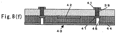
図8(a)〜(g)は、本発明の実施例3−1にかかる多層プリント配線板を製造する工程の一部を示す概略的断面図
図9(a)〜(e)は、本発明の実施例3−1にかかる多層ント配線板を製造する工程の一部を示す概略的断面図
図10(a)〜(d)は、本発明の実施例3−1にかかる多層プリント配線板を製造する工程の一部を示す概略的断面図である。
【発明を実施するための形態】
【0021】
本発明の多層プリント配線板の一実施形態は、半導体素子が収容されている樹脂絶縁層上に、他の樹脂絶縁層と導体回路とが形成され、ビアホールを介して電気的に接続されてなる多層プリント配線板において、前記半導体素子は、樹脂絶縁層に設けた凹部内に収容され、その凹部の周囲に電磁シールド層が形成されていることを特徴とする。
【0022】
本発明の実施形態において、半導体素子を収容する「凹部の周囲」とは、凹部の側面の外側に位置する樹脂絶縁層、凹部の底面に接するまたは凹部の底面の直下に位置する樹脂絶縁層、凹部の開口周縁に位置する樹脂絶縁層もしくは凹部の内壁(底面+側面)のことを意味する。
【0023】
また、「電磁シールド層」とは、基板内で電気信号を伝達する導体回路(ビアホールを含む)との電気的な接続を有していない、電気的に孤立した金属層であり、半導体素子が、他の半導体素子の起動によって、誤作動などを引き起こすことを抑制する等の半導体素子を保護させるシールド効果を有するものを意味する。また、場合によっては、凹部内に収容された半導体素子のシールド性を確保させることができるのであれば、電磁シールド層が電気接続性を有していてもよい。本願におけるシールド層は、半導体素子の周囲に位置する、側面金属層または下部金属層、あるいは側面金属層と下部金属層からなるものであることが望ましい。
【0024】
本発明の実施形態において、電磁シールド層は、その一つの形態として、半導体素子を内蔵する凹部の外側に位置する樹脂絶縁層内の側面金属層である。
【0025】
前記側面金属層としては、複数の非貫通孔の内壁表面に金属を被覆させ、または複数の非貫通孔内に金属を充填させることによって形成することができる。
また、前記側面金属層として、凹部の外側に位置する樹脂絶縁層に形成された金属からなる複数の柱状体として形成することができる。
【0026】
前記非貫通孔の形成方法の一例として、凹部の外側に位置する絶縁層に、レーザ、フォトエッチングなどにより、開口を設け、その開口内をめっきなどの金属で被覆することや、めっき、ペーストなどの導電性材料により、開口内を充填させることで形成させることができるのである。そのような金属としては、一種類もしくは複数の金属を用いることができる。
【0027】
前述の柱状体の形成方法の一例として、予め金属などを所望の形状(円柱、多角形の柱体)に形成した金属体を凹部の外側に位置する絶縁層に打ち込んだり、あるいは該金属体を予め配列させた後に、凹部の外側に位置する絶縁層を形成したりするなどで形成させることができる。
【0028】
前記電磁シールド層は、複数の非貫通孔に金属を被覆させた形態、または複数の非貫通孔内に金属を充填させた形態、もしくは柱状体の形態に形成された各側面金属層の少なくとも一部を互いに連結させた構成としてもよいし、連結されていても、部分的に連結されていなくてもよい。
また、複数の非貫通孔に金属を被覆させた形態、または複数の非貫通孔内に金属を充填させた形態、もしくは柱状体の形態に形成された各側面金属層は、個々に離れて存在していてもよい。また、必要であれば、前記各形態の側面金属層を混在させたものを電磁シールド層として構成してもよい。
【0029】
半導体素子の凹部の外側の絶縁層に側面金属層を形成させることにより、シールド効果を得ることができる。前記各側面金属層は、電気的な接続を持たせてもよいし、電気的な接続を持たせなくてもよい。
ただし、複数の非貫通孔の内壁に金属を被覆させた形態、または複数の非貫通孔内に金属を充填させた形態、もしくは柱状体の形態に形成された側面金属層は、基板内で電子回路を構成する導体回路や、それらの導体回路を電気的に接続されているビアホールには電気的に接続されていないものでもよいし、電気的に接続されているものでもよい。
【0030】
以下、説明する便宜上、上記形態の側面金属層を、「シールドビア(shield−via)」と呼ぶ。このシールドビアによって、凹部内に内蔵された半導体素子の側面を囲むような電磁シールド領域を形成することができるので、電磁干渉の影響を抑えることができる。
【0031】
前記シールドビアは、例えば、基板上方から見た場合に、凹部の開口縁部に平行な方向に沿って直線的に配列させる。もしくは、凹部の開口縁部に平行な方向に対してジグザグに配列(千鳥配列)させたりすることによって、電磁シールド層を形成する。
また、前記シールドビアは、柱状であることが望ましい。この場合、「柱状」とは、円柱形状(横断面が楕円形である形状も含む)や多角柱形状(横断面が三角形、正方形、長方形、五角形、六角形、八角形等である形状も含む)、その他の不規則な横断面を有する細長の筒形状を意味する。特に、横断面が円形(楕円形を含む)であって、基板の厚み方向に細長の筒状の形態に形成することが望ましい。なぜならば、断面円形で細長筒状の導体層は、導体層の同心円状の領域までもシールド可能な領域とすることができるので、半導体素子の厚み方向だけでなく、幅方向への均等な電磁シールド領域を確保できるからである。即ち、基板の厚み方向だけでなく、幅方向へのシールド効果も得やすくなるからである。また、シールドビアに対して、熱などの応力が加わったとしても、応力が集中するポイントがなくなりやすくなり、該ビアの近傍でクラック等の不具合が発生しにくくなるからである。
また、前記シールドビアは、非貫通孔に金属を被覆させた形態や、非貫通孔内に金属を充填させた形態であっても、柱状体の形態と同様の効果を得られる。
さらに、前記複数のシールドビアは、互いに連結された形態で、かつ半導体素子を内蔵する凹部の側面を囲むように配置させることによって、基板の幅方向へのシールド効果をより高めることができる。
前記シールドビアの連結は、図1(a)に示すように、凹部の開口周縁に平行な方向に沿って直線的に配列された状態で連結させてもよい。また、図1(b)に示すように、凹部の開口周縁に平行な方向に対してジグザグに配列された状態(千鳥配列)で連結させてもよい。
【0032】
すなわち、凹部の開口周縁に沿って配置された複数のシールドビアにより電磁シールド層を形成するには、連続してシールドビアを繋げることにより、一枚の金属板であるかのように形成してもよい。それとも、シールドビアを交互に位置をずらしながら配列(千鳥配列)させて、一枚の金属板であるかのように形成してもよい。これらのいずれの形態であっても、半導体素子の周囲を取り囲むように、電気的接続を有しない金属層を形成させることによって電磁シールド層を形成することができるので、凹部に内蔵された半導体素子の側面方向の電磁シールド効果を得ることができる。
【0033】
前記シールドビアの連結は、すべてのシールドビアを連結させた連続的な連結構造であってもよいし、部分的に連結させた部分的な連結構造であってもよい。どちらの形態にしても、半導体素子が埋め込まれた凹部の周囲に電磁シールド層を設けていない実装基板と比較して、半導体素子の側面方向の電磁シールド効果が得られるからである。
【0034】
本発明の実施形態において、電磁シールド層の他の形態としては、半導体素子を内蔵する凹部の底面に位置する樹脂絶縁層内に形成された下部金属層あるいは凹部の底面の直下に位置する樹脂絶縁層内に形成された下部金属層の形態が望ましい。これらの金属層はシート状であることがより望ましい。
【0035】
このようなシート状の電磁シールド層は、半導体素子が内蔵された凹部の底面と同等のサイズ、あるいは底面の面積よりもやや大きなサイズもしくは面積を有して形成されることが望ましい。これによって半導体素子の底面方向の電磁シールド効果が得られる。
【0036】
このシート状のシールド層は、凹部の側面の外側に形成した電磁シールド層、即ち、シールドビアに接続されることが望ましい(図1(a)〜1(b)参照)。
それによって、半導体素子の側面方向および底面方向の電磁シールド効果を得ることができる。その結果、電磁干渉の影響をより効果的に抑えることができ、誤作動等の不具合の発生を抑制することができる。
【0037】
なお、上述したような非貫通孔に導電性材料を充填させてなるシールドビア形態の電磁シールド層や、シート状の電磁シールド層以外にも、基板に設けることがある貫通孔内に導電性材料を充填させてなる形態や、金属板を介在させてなる形態などに形成させてもよい。
【0038】
また、本発明の実施形態において、電磁シールド層のさらに他の形態としては、図1(c)に示すように、半導体素子を内蔵する凹部の少なくとも内壁に形成された金属層の形態とすることができる。即ち、凹部の底面と側面とを覆う金属層、あるいは凹部の底面と側面を覆う金属層に加えて、凹部の側面の上端から開口周縁に沿って延設された金属層の形態をなす電磁シールド層は、凹部内に内蔵される半導体素子のパッケージ樹脂層の外側表面(接続パッドが設けられている上面を除く)の全体を取り囲んでいるので、半導体素子の側面方向および底面方向の電磁シールド効果を同時に得ることができる。
【0039】
前記電磁シールド層の形成に用いられる金属としては、ニッケル、銅、クロムのいずれか1種類、あるいは2種類以上が配合されている金属を用いることが望ましい。
【0040】
これらの金属の一例としては、銅、銅−クロム合金、銅−ニッケル合金、ニッケル、ニッケル−クロム合金、クロムなどが挙げられるが、これら以外の金属を用いてもよい。
【0041】
前記金属層の厚さは、5μm〜20μmが望ましい。その理由は、厚さが5μm未満では、シールド層としての効果を相殺させてしまうことがあるからである。一方、厚さが20μm超では、シールド層の効果を向上させることできないことがあるからである。
【0042】
これらの金属層の形成方法としては、無電解めっき、電解めっき、スパッタリング、蒸着等が望ましい。その理由としては、膜厚の均一な金属膜を形成することが容易であるため、電磁波シールド効果をより得やすいからである。
【0043】
これらの方法により形成されたシールド層は、単層もしくは2層以上の複数層で形成してもよい。複数層で形成する場合には、同一方法による形成でも、異なる方法による形成でもどちらでもよい。シールド層として形成する金属層の種類、厚みなどにより適宜行うことができるのである。これらにより、電磁波シールド効果を劇的に低下させるものではない。
【0044】
本発明の実施形態において、半導体素子を内蔵する凹部の底面に金属層を形成し、この金属層を介して半導体素子が内蔵されることが望ましい。その理由は、凹部の深さを均一にすることが可能となり、それによって半導体素子が凹部内に傾いた状態で収容、内蔵されることがなくなるからである。そのため、半導体素子を収容する基板が樹脂製であっても、半導体素子の接続パッドに接続されるビアホールを樹脂絶縁層に形成する際にも、所望のビアホール形状とすることができると共に、金属層は樹脂絶縁層内に形成されているので、熱応力や外部応力などの影響によって反りが生じることが少なくなる。その結果、半導体素子の接続パッドと、それに接続されたビアホールを含んだ導体回路との電気的接続性や接続信頼性を確保しやすくなるからである。
【0045】
また、下部金属層としては、平坦な表面を有するものであってもよい。それにより、凹部形状の保持性や接着剤との接着性が確保されやすくなる。必要に応じて、下部金属層には粗化面を形成してもよい。これらの粗化面により、下部金属層と接着剤とが密着するので、接着性を確保しやすくなることがある。
また、下部金属層は、銅から形成されることが望ましい。エッチングなどによる加工性がよいことなどである。その中でも圧延銅箔を用いて形成されることが望ましい。下部金属層の平坦性を確保されやすくなるし、下部金属層上に載置される半導体素子との収納性や半導体素子との表層の平坦性を確保しやすくなるからである。
【0046】
さらに詳細に説明すると、半導体素子を収容する凹部が形成される樹脂基板は、主としてガラスエポキシ樹脂などにガラス布等の繊維基材である補強材が含まれている樹脂材料から形成されている。それ故に、ザグリ加工等により凹部を形成した場合には、その凹部の底面では位置によって不規則な凹凸が形成される。
【0047】
その結果、凹部の深さが不均一になりやすい。特に、断面をほぼ矩形に形成した凹部の四隅付近では、他の部分に比して凹部の深さが浅くなりやすい。それ故に、本発明のように、凹部の底面に金属層を形成することによって、凹部の深さの均一化が容易になる。特に、凹部が断面矩形の場合には、四隅付近での凹部の深さも均一化しやすくなる。
【0048】
したがって、凹部に半導体素子を収容する際には、半導体素子が傾くことが少なくなるのである。故に、収容された半導体素子のパッドに接続されるビアホールを樹脂絶縁層に形成する際にも、所望のビアホール形状とすることができる。さらに、金属層は樹脂絶縁層内に収納されるように形成されているので、熱応力や外部応力などの影響によって反りが生じることが少なくなる。その結果、例えば、半導体素子の接続パッドとビアホール等の導体回路との接続不良が起きにくくなるため、電気接続性や接続信頼性が低下しにくくなるのである。
【0049】
また、半導体素子と金属層との間に形成される接着剤層は、厚みを均一にすることが容易となるので、半導体素子の密着性を均等にして、ヒートサイクルなどの信頼性試験を行っても、長期間に亘って密着性が確保されやすくなるのである。
【0050】
なお、前記下部金属層は、凹部の底面の面積よりも大きな面積とし、凹部の側面の外側に形成することもできる。したがって、このように形成された下部金属層は、基板に内蔵された半導体素子の底面方向のシールド効果を発揮することができる。また、側面金属であるシールドビア形態の電磁シールド層と併設することが望ましい。必要に応じて、下部金属層に、側面金属層を接続させてもよい。それにより、電磁シールド層としての効果を確保しやすくなる。
前記下部金属層は、レーザ処理により露出されてもよい。これにより、凹部の厚みが均一になりやすくなるからである。
【0051】
前記凹部内の下部金属層の表層は、シャイニー面であることが望ましい。者に一面であると、下部金属層と半導体素子との密着性が確保しやすくなるし、半導体素子と他の樹脂絶縁層に形成されたバイアホールとの接続性と信頼性が確保しやすいからである。また、下部金属層と半導体素子との間に形成される接着剤層の厚みを均一にすることが容易になり、半導体素子の密着が均一となる等の密着性や電気接続性が確保されやすい。
また、接着剤層が、半導体素子の底面および側面の底部周縁に接触していることが望ましい。接着剤層が半導体素子の底面および側面の底部周縁に接触していることにより、半導体素子の密着性が確保しやすいからである。
【0052】
また、半導体素子を収容するための凹部は、その側面が、図2に示すように、テーパ形状に形成されてもよい。その理由は、凹部内に収容された半導体素子は、側面方向の応力(例えば、熱応力や外部応力等)を受けたとしても、その応力をテーパの上部である樹脂材料で緩和することができるからである。また、凹部内への半導体素子の挿入が容易になるからである。
【0053】
凹部のテーパの形状は、側面と底面とのなす角度のうちの小さい方の角度が約60度以上であり、約90度未満であることが望ましい。テーパの上部である樹脂材料で緩和することができるからである。また、凹部内への半導体素子の挿入が容易になるからである。
【0054】
また、凹部の壁面と半導体素子の側面とで構成される間隙に樹脂層が充填されることが望ましい。樹脂が充填されることにより、半導体素子が安定するために、半導体素子の接続性や信頼性が確保されやすくなるからである。
さらに、凹部の壁面と半導体素子の側面とで構成される間隙に樹脂層が充填され、かつ、樹脂絶縁層と一体化されていてもよい。
【0055】
これにより、ビアホールが形成される他の樹脂絶縁層と、凹部の壁面と半導体素子の側面とで構成される間隙に充填される樹脂絶縁層とが同一材料であると、材料間における熱膨張係数の差などに起因する熱応力の発生を抑えられ、半導体の端部におけるクラック等の不具合が抑えられ、耐久性が確保される。その結果、半導体素子の接続性や信頼性が確保されやすくなるからである。
【0056】
また、本発明の実施形態において、半導体素子のパッド上に、図3または図4に示すような、柱状電極または仲介層を形成することが望ましい。半導体素子のパッドとビアホールとの電気的な接続を容易に行なうことができるからである。
【0057】
半導体素子のパッドは、一般的にアルミニウムなどで製造されているが、特に、パッド上に何らかの金属層などを形成しないアルミパッドの状態では、以下のような問題を引き起こすことがあった。フォトエッチング(露光、現像を経る工程)により層間絶縁層にビアホールを形成させた場合には、露光、現像後にパッドの表層に樹脂が残りやすくなる。また、それに加えて、現像液などの付着や後工程の薬液(例えば、めっき液、酸、アルカリなどの溶液)によりパッドの変色を引き起こす場合があった。そのため、該半導体素子のパッドとビアホールとの電気的接続性や接続信頼性が確保されにくい場合があった。
【0058】
一方、レーザによりビアホールを形成する場合には、アルミニウム製のパッドを焼損する危険がある。また、焼損しない条件でレーザ照射を行うと、パッド上に樹脂残りが発生する場合がある。また、後工程(例えば、酸や酸化剤あるいはエッチング液に浸漬工程、種々のアニール工程等をさす。)を経ると、半導体素子のパッドの変色や溶解が発生する場合もあった。これらにより、半導体素子のパッド周辺での電気的接続性や接続信頼性が確保しにくくなるのである。
【0059】
更に、半導体素子のパッドは、直径40μm程度に作られ、ビアホールはそれより大きい径に作られているために、位置ずれなどが起きやすくなり、パッドとビアホールとの未接続など不具合が発生しやすくなる。そのため、該半導体素子のパッドとビアホールとの電気的接続性や接続信頼性が確保されにくくなる場合がある。
【0060】
これに対して、半導体素子のパッド上に、銅等からなる仲介層を設けることで、ビアホール形成の不具合が解消されて、溶剤の使用が可能となるため、パッド上の樹脂残りを防ぐことができると共に、後工程を経てもパッドの変色や溶解が発生しない。これにより、パッドとビアホールとの電気的な接続性や接続信頼性が低下しにくくなる。更に、半導体素子のダイパッドよりも大きな径の仲介層を介在させることで、パッドとビアホールとを確実に接続させることができる。
【0061】
さらに、仲介層を設けることによって、半導体素子をプリント配線板に埋め込む、収容、収容する前、もしくはその後にでも半導体素子の動作確認や電気検査を容易に行なうことができる。その理由は、半導体素子のパッドよりも大きい仲介層が形成されているので、検査用プローブピンが接触し易くなるからである。それにより、予め製品の可否が判定することができ、生産性やコスト面でも向上させることができる。また、プローブによるパッドの損失や傷なども発生しにくくなる。したがって、半導体素子のパッド上にトランジションを形成することによって、プリント配線板に半導体素子を好適に埋め込み、収容することができる。
【0062】
本発明に用いられる、半導体素子を収容する樹脂絶縁層としては、ガラス布エポキシ樹脂基材、フェノール樹脂基材、ガラス布ビスマレイミドトリアジン樹脂基材、ガラス布ポリフェニレンエーテル樹脂基材、アラミド不織布−エポキシ樹脂基材、アラミド不織布−ポリイミド樹脂基材などから選ばれる硬質な積層基材などを用いることができる。これ以外にも、一般的にプリント配線板で使用されるものを用いることができる。例えば、両面または片面銅張積層板や、金属膜を有しない樹脂板、樹脂フィルム、あるいはそれらの複合材料も用いることができる。
【0063】
前記樹脂基材は、その厚さが、20〜350μmの範囲が望ましい。その理由は、厚さがそのような範囲内であれば、層間絶縁層の絶縁性の確保が容易であるとともに、層間接続性を得ることが容易となるからである。
厚さが20μm未満では、層間絶縁層の絶縁性の確保が困難になりやすいことがある。一方、厚さが350μmを越えると、層間での接続性を得ることができないことがあるからである。
【0064】
本発明において、導体回路、半導体素子を収容させる金属層、および電磁波シールドを形成する金属層としては、銅箔が用いられることが望ましい。その理由は、主として、外形加工に優れ、電気特性にも優れるからである。
【0065】
前記導体回路を形成するための銅箔は、その厚さが、5〜20μmの範囲であることが望ましい。その理由は、銅箔の厚さがそのような範囲内であれば、後述するようなレーザ加工を用いて、絶縁性樹脂基材にビアホール形成用の開口を形成する際に、開口周縁の銅箔の変形が少なくなり、導体回路の形成が容易となるからである。また、エッチングにより、微細な線幅の導体回路パターンを形成することが容易となるからである。銅箔の厚さが5μm未満では、後述するようなレーザ加工を用いて、絶縁性樹脂基材にビアホール形成用の開口を形成する際に、開口周縁の銅箔が変形するおそれがある。あるいは、導体回路を形成しがたくなることがあるからである。一方、銅箔の厚さが20μm超では、エッチングにより、微細な線幅の導体回路パターンを形成し難くなることがあるからである。
【0066】
本発明で用いる銅箔は、ハーフエッチング処理により、その厚みを調整したものでもよい。この場合には、樹脂絶縁層に貼付した銅箔の厚みは、前記の数値よりも大きいものを用い、エッチング後の銅箔の厚みが、5〜20μmとなるように調整することが望ましい。
さらに、両面銅張積層版の場合では、銅箔厚みが前記の範囲内であるが、両面で厚みが異なっていてもよい。それにより、強度を確保したりして後工程を阻害しないようにすることができる。
【0067】
また、前記凹部の底面に形成される金属層としての銅箔の厚さは、5〜20μmが望ましい。その理由は、銅箔の厚さがそのような範囲内であれば、キャビティの外形加工を行なう場合に、該銅箔を貫通してしまうおそれが少なくなるので、凹部の底面への金属層の形成が妨げられることが少なくなる。また、エッチングによる金属層の加工形成が容易になるからである。
前記凹部の底面に形成される金属層としては、銅以外にも、ニッケル、鉄、コバルトなどの金属を用いてもよい。
【0068】
また、電磁シールド層を形成するシート状の金属層としての銅箔の厚さは、5〜20μmが望ましい。その理由は、銅箔の厚さがそのような範囲内にあれば、シールド効果の確保しやすくなるからである。
【0069】
なお、前記絶縁性樹脂基材および銅箔としては、特に、エポキシ樹脂をガラスクロスに含潰させてBステージとしたプリプレグと、銅箔とを積層して加熱プレスすることにより得られる片面もしくは両面銅張積層板を用いることが好ましい。その理由は、銅箔がエッチングされた後の取扱中に、配線パターンやビアホールの位置がずれることがなく、位置精度に優れるからである。
【0070】
本発明において、半導体素子を収容するために樹脂絶縁層に設ける凹部は、ザグリ加工、パンチング、レーザ加工等によって形成することができる。特に、レーザ加工によって形成されることが望ましい。それにより、他の加工と比較して、均一な深さの凹部が形成しやすくなる。
【0071】
前記凹部をレーザ加工によって形成する場合は、レーザ照射による加熱により金属層(銅箔)の表面に酸化膜が形成され、密着性を向上させることができることもある。また、レーザ加工は、凹部をテーパ形状に加工しやすいいのである。
また、ザグリ加工によって凹部を形成する場合には、凹部の底面に形成した金属層がストッパーの役目を果たすので、凹部の深さを均一にすることができる。
【0072】
前記凹部の深さは、収容される半導体素子自体の厚みおよびその半導体素子の接続パッド上に形成されることがある柱状電極あるいは仲介層の厚み、接着剤層の厚みなどに応じて決められる。そして、凹部の底部には金属層が形成されるので、半導体素子と樹脂絶縁層との間に設けられる接着剤層の厚みを均一にすることが容易となる。その結果として、半導体素子を収容した際に、半導体素子の傾きなどを少なくすることができるのである。
【0073】
また、半導体素子と樹脂絶縁層との密着性を均一に保持することができるので、ヒートサイクルなどの信頼性試験を行っても、長期間に亘って密着性が低下し難くなる。
【0074】
また、半導体素子を収容するための凹部は、その側面を底面から上方に向かうにつれて末広がりとなるようなテーパを有する形状に形成されることが望ましい。そのような形状とすることで、凹部内に収容された半導体素子は、側面方向の応力(例えば、熱応力や外部応力等)を受けても、その応力を緩和することができる。さらに、半導体素子を固着させるために半導体素子の底面に設けた接着剤が、毛管現象によって凹部の側面に沿って流動することが少なくなるので、半導体素子の凹部底部への密着性が低下しにくくなる。
【0075】
本発明において、テーパの角度は、図2に示すように、側面と底面とがなす外角で定義され、そのテーパの角度は、60度以上、90度未満であることが望ましく、60度〜85度の範囲がより望ましい。その理由は、テーパ角度がそのような範囲内であれば、半導体素子の側面における応力により移動を抑制することが相殺されることが少なくなるために、信頼性試験を行った場合に、ビアホールの接続不具合が起こりにくくなるからである。テーパ角度が60度未満では、半導体素子の側面における応力により移動を抑制することが相殺されることもあり、そのために、信頼性試験を行うと、ビアホールの接続不具合が早期に引き起こしたりすることがあるからである。
【0076】
本発明において、半導体素子を収容する絶縁樹脂層の一実施形態としては、上述したような絶縁性樹脂基材を2枚用いる、即ち、一方の表面に半導体素子収容用凹部の底面のサイズよりも大きなサイズの金属層が形成された第一絶縁性樹脂基材と、その第一絶縁性樹脂基材の金属層が形成された側の表面に第二絶縁性樹脂基材とを積層し、第一絶縁性樹脂基材の他方の表面に対してレーザ照射を行って、金属層に達する半導体素子収容用凹部およびその凹部の側面の外側にシールドビア形成用の複数の非貫通孔を形成することで、その凹部の底面および非貫通孔の底面から金属層が露出するようにした後、非貫通孔に金属めっきを充填することによって、電磁シールド層としてのシールドビアを凹部の側面の外側に形成してなる半導体収容用基板を形成する。
【0077】
また、他の実施形態としては、一方の表面に半導体素子収容用凹部の底面のサイズよりも大きなサイズの金属層が形成されてなる第二絶縁性樹脂基材と、金属層に対応する領域に半導体素子のサイズにほぼ相当する大きさの開口が形成されてなる第一絶縁性樹脂基材とを積層して、開口の一方が塞がれた形態の半導体素子収容用凹部を形成した後、第一絶縁性樹脂基材の表面に対してレーザ照射を行って、金属層に達する複数の非貫通孔を形成することで、その非貫通孔の底面から金属層が露出するようにした後、非貫通孔に金属めっきを充填することによって、電磁シールド層としてのシールドビアを凹部の側面の外側に形成してなる半導体収容用基板を形成してもよい。
【0078】
さらに他の実施形態としては、一方の表面に半導体素子収容用凹部の底面のサイズよりも大きなサイズの金属層が形成された第一絶縁性樹脂基材の、その金属層が形成された側の表面に第ニ絶縁性樹脂基材を積層し、第一絶縁性樹脂基材の他方の表面に対してレーザ照射を行って、金属層に達する半導体素子収容用凹部を形成することで、その凹部の底面から金属層が露出するようにした後、その凹部の内壁面全体にめっき、あるいはスパッタリングにより金属被覆層を形成することによって電磁シールド層を形成してなる半導体収容用基板を形成する。
【0079】
このような実施形態では、第一の絶縁性樹脂基材および第二の絶縁性樹脂基材の厚さは、20〜350μmであることが望ましい。その理由は、厚さがそのような範囲内では、層間絶縁層の絶縁性の確保および層間接続を行うビアホールの形成が容易となり、電気接続性の低下を招くことが少なくなるからである。
【0080】
また、それぞれの絶縁性樹脂基材としては、単層からなる樹脂基材を用いてもよいし、複数層に多層化した樹脂基材を用いてもよい。
【0081】
前記半導体収容基板の凹部内用に半導体素子を埋め込んで収容させた後、半導体収容用基板の片面もしくは両面に層間樹脂絶縁層を形成し、次いでその層間樹脂絶縁層に、半導体素子との電気的接続をなすビアホールを含んだ導体回路を形成した後、更に他の層間樹脂絶縁層と導体回路とを交互に積層することによって、本発明にかかる多層プリント配線板を製造することができる。
【0082】
前記半導体収容基板の凹部内に埋め込む半導体素子としては、その接続パッド上に予め柱状電極が形成された半導体素子、あるいは接続パッドを被覆する仲介層が形成された半導体素子のいずれでも用いることができ、これらの半導体素子は、柱状電極あるいは仲介層を介して層間樹脂絶縁層に設けたビアホールに電気的に接続される。
【0083】
以下、(1)柱状電極を有する半導体素子および(2)仲介層を有する半導体素子の製造方法について説明する。
(1)柱状電極を有する半導体素子の製造方法
本発明で用いる柱状電極を有する半導体素子とは、柱状電極あるいは再配線を有する半導体素子を意味する。
図3に示すように、ウエハ状態の半導体素子1(シリコン基板)上にアルミニウムなどからなる接続パッド2を形成し、その上面において接続パッド2の中央部を除く部分に保護膜3(パッシベーション膜)を形成したものを用意する。この状態では、接続パッド2の表面は、保護膜3に被覆されていない中央部において露出している。
【0084】
次に、半導体素子1の上面全体に下地金属層4を形成する。下地金属層としては、クロム、銅、ニッケルなどを用いることができる。
次いで、下地金属層4の上面に液状レジストからなるメッキレジスト層を形成し、メッキレジスト層の半導体素子の接続パッドに対応する部分に開口部を形成する。
【0085】
次いで、下地金属層4をメッキ電流路として電解メッキを行うことにより、メッキレジスト層の開口部内の下地金属層の上面に柱状電極5を形成する。その後、メッキレジスト層を剥離し、さらに、柱状電極5をマスクとして下地金属層の不要な部分をエッチングして除去すると、柱状電極下にのみ下地金属層4が残存される。
【0086】
さらに、半導体素子1の上面側にエポキシ樹脂やポリイミド等からなる封止膜6を形成する。この状態において、柱状電極5の上面が封止膜6によって覆われた場合には、表面を適宜に研磨することにより、柱状電極5の上面を露出させる。次に、ダイシング工程を経ると、個々の半導体チップ(柱状電極を有する半導体素子)が得られる。
【0087】
(2)仲介層を有する半導体素子の製造方法
本発明において用いられる仲介層とは、半導体素子のパッド上に設けられるビアホールとの電気的な接続を行うための介在層を意味する。
【0088】
図4に示すように、内蔵する半導体素子10の全面に蒸着、スパッタリングなどを行い、全面に導電性の金属層12(第1薄膜層)を形成させる。その金属としては、スズ、クロム、チタン、ニッケル、亜鉛、コバルト、金、銅などがよい。厚みとしては、0.001〜2.0μmの間で形成させるのがよい。その理由は、金属層の厚みがそのような範囲内であれば、全面に均一な膜厚の金属層を形成することが容易となり、膜厚のバラツキが少なくなるからである。
【0089】
上記第1薄膜層12により、接続パッド14が被覆され、仲介層20と半導体素子の接続パッド14の界面の密着性を高めることができる。また、これらの金属で半導体素子10の接続パッド14を被覆することで、界面への湿分の侵入を防ぎ、パッドの溶解、腐食を防止し、信頼性を低下させにくくすることができる。
【0090】
第1薄膜層12の金属としては、クロム、ニッケル、チタンのいずれかの金属を用いることが望ましい。その理由は、接続パッド14と金属層12との密着性がよく、また、界面への湿分の侵入を防止しやすいからである。
第1薄膜層12上に、スパッタ、蒸着、または無電解めっきにより第2薄膜層17を形成させる。その金属としてはニッケル、銅、金、銀などがある。電気特性、経済性、あるいは後工程で形成される厚付け層が主として銅から形成されることから、第2薄膜層17も銅を用いて形成することが望ましい。
【0091】
ここで第2薄膜層17を設ける理由は、第1薄膜層12だけでは、後述する厚付け層を形成するための電解めっき用のリードを取ることが難しいためである。第2薄膜層17は、厚付けのリードとして用いられる。
第2薄膜層17の厚みは、0.01〜5.0μmの範囲が望ましい。その理由は、厚さがそのような範囲内では、リードとしての役割を果たすことができるとともに、エッチングの際、下層の第1薄膜層がより多く削れて隙間ができるということが少なくなるので、湿分が侵入し難くなり、信頼性の低下を招くことがないからである。
前記第2薄膜層17上に、無電解あるいは電解めっきにより厚付けさせる。形成される金属の種類としてはニッケル、銅、金、銀、亜鉛、鉄などがある。電気特性、経済性、仲介層としての強度や構造上の耐性、あるいは後工程で形成されるビルドアップ配線層の導体層は主として銅から形成されることから、電解銅めっきにより形成することが望ましい。
【0092】
厚付け電解銅めっき層18の厚みは、1〜20μmの範囲が望ましい。その理由は、厚さがそのような範囲内では、上層のビアホールとの接続信頼性が低下することが少なくなるからである。また、エッチングの際にアンダーカットが生じることが少なくなり、形成される仲介層とビアホールの界面に隙間が発生することが少なくなる。
【0093】
その後、エッチングルジストを形成して、露光、現像して仲介層以外の部分の金属を露出させてエッチングを行い、半導体素子のパッド上に第1薄膜層12、第2薄膜層17、厚付け層18からなる仲介層20を形成させる。
【0094】
上記仲介層の製造方法以外にも、基板の凹部内に半導体素子を内蔵した後、仲介層を形成してもよいし、半導体素子およびコア基板の上に形成した金属膜上にドライフィルムレジストを形成して仲介層に該当する部分を除去させて、電解めっきによって厚付けした後、レジストを剥離してエッチング液によって、同様に半導体素子のダイパッド上に仲介層を形成させることもできる。
【0095】
次に、本発明にかかる多層プリント配線板を製造する方法の一例について、具体的に説明する。
A.半導体素子収容用基板の作製
本発明にかかる多層プリント配線板を製造するに当たって、それを構成する半導体素子収容用基板としては、絶縁性樹脂基材の片面もしくは両面に銅箔が貼付けられてなる第一の絶縁性樹脂基材と第二の絶縁性樹脂基材とを積層した形態のものを用いる。
【0096】
(1)前記第一絶縁性樹脂基材は、例えば、両面銅張積層板から形成することができ、このような両面銅張積層板の一方の表面にレーザ照射を行って、一方の銅箔および樹脂絶縁層を貫通して他方の銅箔の裏面に達するビアホール形成用開口およびシールドビア形成用開口を形成する。
このとき、シールドビア形成用開口は、後述するような半導体素子収容用凹部の形成領域の外側に形成され、隣接する開口どうしが連結した形態に形成される。
【0097】
前記レーザ照射は、パルス発振型炭酸ガスレーザ加工装置を用いて行われ、その加工条件は、パルスエネルギーが0.5〜100mJ、パルス幅が1〜100μs、パルス間隔が0.5ms以上、周波数2000〜3000Hz、ショット数が1〜5の範囲内であることが望ましい。
【0098】
このような加工条件のもとで形成され得る開口径は、20〜250μmであることが望ましい。その理由は、口径がそのような範囲内では、ビアホール形成が技術的に容易になり、電気接続性の低下を招くことが少なくなるからである。また、めっきによる充填が容易になるので、電気接続性の低下を招くことが少なくなり、配線の高密度化が容易になるからである。口径が20μm未満では、ビアホール形成が技術的に困難になることがあり、電気接続性が確保しにくくなることがある。一方、口径が250μmを超えると、めっきでの充填性に難があることがあり、電気接続性が確保されないことがあるし、配線の高密度化を阻害することもあるからである。
【0099】
なお、レーザ照射によって銅張積層板にビアホール形成用開口およびシールドビア形成用開口を形成させるには、銅箔と絶縁性樹脂基材とに同時に開口を形成するようなレーザ照射を行うダイレクトレーザ法と、ビアホール形成用開口に該当する銅箔部分をエッチングにより予め除去した後に、絶縁性樹脂基材にビーム照射を行うコンフォーマル法があり、そのどちらを用いてもよい。
【0100】
(2)前記工程で形成された開口内に残留する樹脂残滓を除去するために、デスミア処理を行うことが望ましい。
このデスミア処理は、酸あるいは酸化剤(例えば、クロム酸、過マンガン酸)の薬液処理等の湿式処理や、酸素プラズマ放電処理、コロナ放電処理、紫外線レーザ処理またはエキシマレーザ処理等の乾式処理によって行われる。
これらのデスミア処理を選択する方法は、絶縁性樹脂基材の種類や、厚み、開口径、レーザ条件等により残留が予想されるスミア量に応じて選ばれる。
【0101】
(3)前記デスミア処理した基板のビアホール形成用開口および側面金属層であるシールドビア形成用開口に対して、銅箔をめっきリードとする電解銅めっき処理を施して、ビアホール形成用開口およびシールドビア形成用開口内に電解銅めっきを完全に充填して、ビアホール(フィルドビア)およびシールドビアが形成される。
なお、場合によっては電解銅めっき処理の後、基板の開口上部に盛り上がった電解銅めっきを、ベルトサンダー研磨、バフ研磨、エッチング等によって除去して平坦化してもよい。
【0102】
(4)前記第一の絶縁性樹脂基材の両面にレジスト層を形成し、露光・現像工程を経て、レジスト非形成部分に対して、塩化第二銅などからなるエッチング液により、エッチング処理を行う。その後、レジストを剥離することにより、第一の絶縁性樹脂基材の一方の表面には、ビアホールランドを含んだ導体回路、位置合わせ用の位置決めマーク等が形成され、他方の表面には、半導体素子に関連したサイズを有する金属層、ビアホールランドを含んだ導体回路、位置合わせ用の位置決めマーク等が形成される。
なお、複数のシールドビアは互いに連結された形態に形成され、それらの一端は、第一の絶縁性樹脂基材の一方の表面に露出しており、他方は金属層表面に接続されて、電磁シールド層を形成している。
【0103】
(5)前記第一の絶縁性樹脂基材の金属層が形成された側の表面に第二の絶縁性樹脂基材を積層する。
例えば、接着剤層であるプリプレグに銅箔を重ね合わせたものから第二の絶縁性樹脂基材を形成し、それを第一の絶縁性樹脂基材の片面に熱圧着により積層してなる積層体を形成する。
【0104】
(6)前記積層体を構成する第一絶縁性樹脂基材の金属層を設けた面に、前記(1)と同様にレーザ照射を行って、第二絶縁性樹脂基材の銅箔表面を貫通すると共に樹脂層を通過して、第一絶縁性樹脂基材に形成したビアホールランドを含んだ導体回路に達するビアホール形成用の開口を形成する。
【0105】
このビアホール形成用開口の加工条件は、パルスエネルギーが0.5〜100mJ、パルス幅が1〜100μs、パルス間隔が0.5ms以上、周波数2000〜3000Hz、ショット数が1〜10の範囲内であることが望ましい。
また、前記加工条件のもとで形成され得るビアホール形成用開口の口径は、20〜250μmであることが望ましい。その理由は、口径がそのような範囲内では、ビアホール形成が技術的に容易になり、電気接続性の低下を招くことが少なくなるからである。また、めっきによる充填が容易になるので、電気接続性の低下を招くことが少なくなり、配線の高密度化が容易になるからである。
【0106】
(7)前記(6)の工程で形成されたビアホール形成用開口内に残留する樹脂残滓を除去するために、前記(2)と同様にデスミア処理を行う。
【0107】
(8)次に、前記第一絶縁性樹脂基材の表面を保護フィルムにより被覆した状態で、前記デスミア処理した基板の銅箔面に対して、その銅箔をめっきリードとする電解銅めっき処理を施して、開口内に電解銅めっきを完全に充填し、フィルドビアを形成する。
【0108】
なお、場合によっては電解銅めっき処理の後、基板のビアホール形成用開口の上部に盛り上がった電解銅めっきを、ベルトサンダー研磨、バフ研磨、エッチング等によって除去して平坦化してもよい。
また、無電解めっきを経て、電解めっきを形成してもよい。この場合には、無電解めっき膜は、銅、ニッケル、銀等の金属を用いてもよい。
【0109】
(9)前記電解銅めっき膜上に、レジスト層を形成する。レジスト層は、塗布でも予めフィルム状にしたものを貼り付けるいずれの方法でもよい。このレジスト上に予め回路が描画されたマスクを載置して、露光、現像処理してエッチングレジスト層を形成し、エッチングレジスト非形成部分の金属層をエッチングして、ビアホールランドを含んだ導体回路を形成し、その後、前記(8)の工程で貼付した保護フィルムを剥離させる。
このエッチング液としては、硫酸一過酸化水素、過硫酸塩、塩化第二銅、塩化第二鉄の水溶液から選ばれる少なくとも1種の水溶液が望ましい。
【0110】
前記銅箔をエッチングして導体回路を形成する前処理として、ファインパターンを形成しやすくするため、あらかじめ、銅箔の表面全面をエッチングして厚さを調整してもよい。
前記導体回路の一部としてのビアホールランドは、その内径がビアホール口径とほぼ同様であるか、その外径をビアホール径よりも大きく形成し、ランド径を50〜350μmの範囲に形成することが好ましい。その理由は、その理由は、ランド径がそのような範囲内では、ビアホールとランドの接続が阻害されることが少なくなるとともに、高密度化を阻害することも少なくなるからである。
【0111】
(10)次いで、第一絶縁性樹脂基材の金属層を設けた面と反対側の表面領域(半導体素子収容領域)に、例えば、レーザ加工によって樹脂層を貫通して金属層表面に達する開口を形成し、その開口から金属層表面が露出するような凹部を形成して、半導体素子収容用基板とする。必要に応じて、レジスト形成工程、エッチング処理工程を経て、金属層が露出されるような凹部を形成することもできる。
例えば、前記第一絶縁性樹脂基材と第二絶縁性樹脂基材との積層体に、パルス発振型炭酸ガスレーザ加工装置を用いたレーザ照射によって、第一絶縁性樹脂基材の表面から樹脂層を貫通して金属層表面に達する開口を形成して半導体素子を収容または内蔵させる凹部を形成する。
【0112】
前記半導体素子を収容する凹部の加工条件は、パルスエネルギーが0.5〜100mJ、パルス幅が1〜100μs、パルス間隔が0.5ms以上、周波数2000〜3000Hz、ショット数が1〜10の範囲内であることが望ましい。
このようなレーザ加工により、半導体素子を内蔵させる凹部が形成され、該凹部の底面には、金属層(この場合は、銅箔を指す。)が露出される。
【0113】
B.半導体素子の収容、埋め込み
(11)前記A.の(1)〜(10)の工程により得られた半導体素子収容用基板に、半導体素子を埋め込む。
この埋め込まれる半導体素子としては、前述したように、接続パッド上に予め柱状電極が形成された半導体素子、あるいは接続パッドを被覆する仲介層が形成された半導体素子のいずれをも用いることができるが、ここでは後者を用いる場合について説明する。
【0114】
この仲介層は、半導体素子のパッドとプリント配線板のビアホールを含む導体回路とを直接的に接続させるために設けられた仲介層であり、ダイパッド上に、薄膜層を設け、その薄膜層上にさらに厚付け層を設けることによって形成され、少なくとも2層以上の金属層で形成することが好ましい。
また、この仲介層は、半導体素子のダイパッドよりも大きなサイズに形成されることが好ましい。そのようなサイズにすることによって、ダイパッドとの位置合わせが容易となり、その結果、ダイパッドとの電気的接続性が向上すると共に、ダイパッドにダメージを与えることなくレーザ照射やフォトエッチングによるビアホール加工が可能となる。そのため、半導体素子のプリント配線板への埋め込み、収容、収容や電気的な接続を確実に行うことができる。
また、仲介層上には、直接、プリント配線板の導体回路をなす金属層を形成することが可能となる。
また、仲介層は、前述したような製造方法以外にも、半導体素子の接続パッド側の全表面または半導体素子を埋め込んだ半導体素子収容用基板上に形成した金属膜上に、ドライフィルムからなるレジストを形成し、仲介層に該当する部分を除去させた後、電解めっきによって厚付けし、その後、レジストを剥離してエッチング液によって、同様に半導体素子の接続パッド上に仲介層を形成させることもできる。
【0115】
(12)半導体素子を収容、内蔵した基板上に、絶縁樹脂層を設けた後、前記A.の(1)〜(4)と同様の処理を行うことにより、内蔵された半導体素子の接続パッド上に形成した仲介層に電気的に接続されるビアホール、半導体素子収容用基板に形成されたビアホールを含む導体回路に電気的に接続されるビアホール、および外側の導体回路を形成することができる。さらに、絶縁樹脂層と銅箔を積層させ、前記A.の(1)〜(4)と同様の処理を繰り返し行うことにより、更に多層化したプリント配線板を得ることができる。
【0116】
前述の方法は、絶縁樹脂層の積層を逐次積層することにより絶縁樹脂層の多層化を行ったが、必要に応じて、絶縁樹脂層が1単位の回路基板を2層以上に積層し、一括で加熱圧着することによって、絶縁樹脂層の多層化を行うような多層プリント配線板としてもよい。
【0117】
(13)次に、最も外側の回路基板の表面にソルダーレジスト層をそれぞれ形成する。この場合、回路基板の外表面全体にソルダーレジスト組成物を塗布し、その塗膜を乾燥した後、この塗膜に、半田パッドの開口部を描画したフォトマスクフィルムを載置して露光、現像処理することにより、導体回路のビアホール直上に位置する導電性パッド部分を露出させた半田パッド開口をそれぞれ形成する。この場合、ソルダーレジスト層をドライフィルム化したものを貼り付けて、露光・現像もしくはレーザ加工により開口を形成させてもよい。
【0118】
前記マスク層の非形成部から露出した半田パッド上に、ニッケル−金などの耐食層を形成する。このとき、ニッケル層の厚みは、1〜7μmが望ましく、金層の厚みは0.01〜0.1μmが望ましい。
これ以外にも、ニッケル−パラジウム−金、金(単層)、銀(単層)等を形成してもよい。耐食層を形成した後に、マスク層を剥離する。これにより、耐食層を形成された半田パッドと耐食層が形成されていない半田パッドとが混在するプリント配線板となる。
【0119】
(14)前記(13)の工程で得られたソルダーレジストの開口からビアホール直上に露出した半田パッド部分に、半田体を供給し、この半田体の溶融・固化によって半田バンプを形成し、あるいは導電性ボールまたは導電性ピンを導電性接着剤もしくは半田層を用いてパッド部に接合して、多層回路基板が形成される。
【0120】
前記半田体および半田層の供給方法としては、半田転写法や印刷法を用いることができる。
ここで、半田転写法は、プリプレグに半田箔を貼合し、この半田箔を開口部分に相当する箇所のみを残してエッチングすることにより、半田パターンを形成して半田キャリアフィルムとし、この半田キャリアフィルムを、基板のソルダーレジスト開口部分にフラックスを塗布した後、半田パターンがパッドに接触するように積層し、これを加熱して転写する方法である。
【0121】
一方、印刷法は、パッドに相当する箇所に開口を設けた印刷マスク(メタルマスク)を基板に載置し、半田ペーストを印刷して加熱処理する方法である。このような半田バンプを形成する半田としては、Sn/Ag半田、Sn/In半田、Sn/Zn半田、Sn/Bi半田などが使用でき、それらの融点は、積層される各回路基板間を接続する導電性バンプの融点よりも低いことが望ましい。
【実施例】
【0122】
(実施例1−1)
(1)基材の準備
まず、半導体素子収容用基板を構成するプリント基板を製作する。このプリント基板は、第一絶縁性基材30と第二絶縁性基材40からなり、それらの基材を積層して形成する。プリント基板の材質の一例としては、エポキシ系樹脂をガラスクロスに含潰させてBステージとしたプリプレグと、銅箔とを積層して加熱プレスすることにより得られる片面または両面銅張積層板を出発材料として用いる。
前記第一絶縁性基材30として、厚みが60μmの樹脂絶縁層32の両面に、厚みが15μmの銅箔34を貼付してなる両面銅張積層板を用いる。この積層板の銅箔32が15μmよりも厚いものを用いて、エッチング処理により、銅箔の厚みを15μmに調整してもよい(図5(a)参照)。
【0123】
(2)ビアホールおよびシールドビア形成用開口の形成
前記第一絶縁性基材30の一方の銅箔表面に、炭酸ガスレーザ照射を行って、銅箔34および樹脂絶縁層32を貫通して他方の銅箔表面に達するビアホール形成用開口36およびシールドビア形成用開口37を形成した(図5(b)参照)。
【0124】
このとき、シールドビア形成用開口37(非貫通孔)は、後述するような半導体素子収容用凹部の形成領域の外側に形成され、隣接する開口どうしが互いに直列に連結した形態に形成される。
さらにその開口内を過マンガン酸の薬液処理によってデスミア処理した。
【0125】
この実施例においては、ビアホール形成用の開口36およびシールドビア形成用開口37の形成には、日立ビア社製の高ピーク短パルス発振型炭酸ガスレーザ加工機を使用し、基材厚60μmのガラス布エポキシ樹脂基材に、銅箔にダイレクトに、以下のような照射条件で、レーザビームを照射して100穴/秒のスピードで、直径75μmのビアホール形成用開口36およびシールドビア形成用開口37を形成した。
【0126】
(照射条件)
パルスエネルギー:0.5〜100mJ
パルス幅:1〜100μs
パルス間隔:0.7ms
周波数:2000Hz
【0127】
(3)電解銅めっき膜の形成
デスミア処理を終えた第一絶縁性基材30のビアホール形成用開口36およびシールドビア形成用開口37を設けた銅箔面に、以下のようなめっき条件で、銅箔をめっきリードとする電解銅めっき処理を施した。
【0128】
〔電解めっき液〕
硫酸 2.24mol/l
硫酸銅 0.26mol/l
添加剤A(反応促進剤) 11.0ml/l
添加剤B(反応抑制剤) 10.0ml/l
【0129】
〔電解めっき条件〕
電流密度 1A/dm2
時間 65分
温度 22±2℃
【0130】
このようなめっき処理によって、添加剤Aにより開口内の電解銅めっき膜の形成が促進され、逆に添加剤Bにより主として銅箔部分に付着されて、めっき膜の形成を抑制される。また、開口内が電解銅めっきで充填されて、銅箔とほぼ同一の高さになると、添加剤Bが付着されるので、銅箔部分と同様にめっき膜の形成が抑制される。これにより、開口内に完全に電解銅めっきが充填されると共に、開口から露出した電解銅めっきと銅箔とがほぼ平坦に形成された(図5(c)参照)。
また、銅箔および電解めっき膜からなる導体層をエッチングによって、厚みを調整してもよい。場合によってはサンダーベルト研磨およびバフ研磨の物理的方法によって導体層の厚みを調整してもよい。
【0131】
(4)導体回路(フィルドビアを含む)、シールドビアおよび金属層の形成
前記(3)の工程を経た第一絶縁性基材30の銅箔34および銅めっき膜上に、感光性ドライフィルムを用いてエッチングレジスト層(図示を省略)を形成した。即ち、第一絶縁性基材30の両面の銅箔面にエッチングレジスト層を形成した。そのレジスト層の厚みは、15〜20μmの範囲であり、ランドを含む導体回路および半導体素子のサイズに関連したサイズの金属層が描画されたマスクを用いて、露光・現像を経て、銅箔上にレジスト非形成部を形成した。
次いで、レジスト非形成部に、過酸化水素水/硫酸からなるエッチング液により、エッチングを行い、非形成部に該当する銅めっき膜および銅箔を除去する。
【0132】
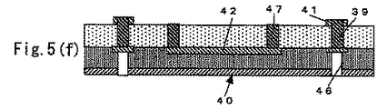
その後、レジストをアルカリ液により剥離することによって、フィルドビア39のランドを含む導体回路41、金属層42、シールドビア47が形成される。必要に応じて、ダミーパターンや、アライメントマーク、製品認識記号等を形成することができる。
なお、この工程においては、複数のシールドビア47は、図1(a)に示されるような直列に連結された形態となり、金属層42の表面に接続されて、電磁シールド層を形成する。
【0133】
これによって、第一絶縁性基材30の表面と裏面に導体回路41が形成されると共に、これらの導体回路41を電気的に接続するフィルドビア39が形成され、さらに、半導体素子に接触する金属層42が形成され、そして金属層42の表面に接続されて電磁シールド層を構成するシールドビア47が形成されてなる回路基板が得られる。
【0134】
なお、この回路基板に形成される金属層42は、第一絶縁性基材の裏面に形成され、半導体素子を収容する凹部を形成する領域に相当する回路基板表面の銅箔部分はエッチングにより除去される(図5(d)参照)。
【0135】
(5)第一絶縁性基材と第二絶縁性基材との積層
前記第一絶縁性基材30に積層される第二絶縁性基材40としては、厚みが60μmの樹脂絶縁層43の片面に、厚みが15μmの銅箔44が貼付されてなる片面銅張積層板を用いる。
【0136】
このような第二絶縁性基材40は、銅箔が形成されていない側の表面が第一絶縁性基材30の金属層42が形成された表面に接触した状態で積層される。第一絶縁性基材30と第二絶縁性基材40の積層は、以下のような条件で両者を熱圧着することにより行われる(図5(e)参照)。
【0137】
(圧着条件)
温度:150〜180℃
プレス圧力:100〜200kgf/cm2
圧着時間:5〜10分
【0138】
なお、この実施例では、第一絶縁性基材30および第二絶縁性基材40を単層で形成させたが、2層以上の複数層で形成してもよい。
【0139】
(6)ビアホール形成用開口の形成
前記第二絶縁性基材40の銅箔形成面に対して、炭酸ガスレーザ照射を行って、銅箔44を貫通すると共に、樹脂絶縁層43を通過して、前記第一絶縁性基材30に設けたフィルドビア39のビアランドを含む導体回路41表面に達するビアホール形成用開口46を形成した(図5(f)参照)。さらに、それら開口内を過マンガン酸の薬液処理によってデスミア処理した。
【0140】
この実施例において、第二絶縁性基材40にビアホール形成用の開口46を形成するには、日立ビア社製の高ピーク短パルス発振型炭酸ガスレーザ加工機を使用した。第二絶縁性基材40の基材厚60μmのガラス布エポキシ樹脂基材43に貼付された銅箔44にダイレクトに、以下のような照射条件で、レーザビームを照射して100穴/秒のスピードで、直径75μmのビアホール形成用の開口46を形成した。
【0141】
(照射条件)
パルスエネルギー:0.5〜100mJ
パルス幅:1〜100μs
パルス間隔:0.7ms
周波数:2000Hz
【0142】
(7)電解銅めっき膜の形成
前記第一絶縁性基材30の表面を保護フィルム48を貼付して被覆した後、開口内のデスミア処理を終えた第二絶縁性基材40の銅箔面に、以下のような組成の電解めっき液溶液を用いて、銅箔をめっきリードとする電解銅めっき処理を施した。
【0143】
〔電解めっき液〕
硫酸 2.24mol/l
硫酸銅 0.26mol/l
添加剤A(反応促進剤) 11.0ml/l
添加剤B(反応抑制剤) 10.0ml/l
【0144】
〔電解めっき条件〕
電流密度 1A/dm2
時間 65分
温度 22±2℃
【0145】
このようなめっき処理においては、添加剤Aにより開口内の電解銅めっき膜の形成が促進され、逆に添加剤Bにより主として銅箔部分に付着されて、めっき膜の形成を抑制される。また、開口内が電解銅めっきで充填されて、銅箔とほぼ同一の高さになると、添加剤Bが付着されるので、銅箔部分と同様にめっき膜の形成が抑制される。これにより、開口内に完全に電解銅めっきが充填されると共に、開口から露出した電解銅めっきと銅箔とがほぼ平坦に形成された。
また、銅箔、電解めっき膜からなる導体層をエッチングによって、厚みを調整してもよい。場合によってはサンダーベルト研磨およびバフ研磨の物理的方法によって導体層の厚みを調整してもよい。
【0146】
(8)導体回路およびフィルドビアの形成
前記(7)の工程を経た第二絶縁性基材40の銅箔44および銅めっき上に、感光性ドライフィルムを用いてエッチングレジスト層(図示を省略)を形成した。このレジスト層の厚みは、15〜20μmの範囲であり、フィルドビアのランドを含む導体回路が描画されたマスクを用いて、露光・現像を経て、銅箔上にレジスト非形成部を形成した。
【0147】
次いで、レジスト非形成部に、過酸化水素水/硫酸からなるエッチング液により、エッチングを行い、非形成部に該当する銅めっき膜および銅箔を除去する。
【0148】
その後、レジストをアルカリ液により剥離し、さらに、前記(7)の工程にて第一絶縁性基材30の表面に貼付した保護フィルム48を剥離させることによって、第二絶縁性基材40の片面に導体回路50が形成されると共に、これらの導体回路を第一絶縁性基材30に設けたフィルドビア39のランド41に電気的に接続するフィルドビア52が形成される(図5(g)参照)。必要に応じて、ダミーパターンや、アライメントマーク、製品認識記号等を形成することもできる。
【0149】
(9)半導体素子収容用凹部の形成
前記(4)の工程で、エッチングによって銅箔部分が除去されている樹脂部分に、炭酸ガスレーザ照射を行って、樹脂層を貫通して金属層表面に達する開口を形成し、その開口内に金属層が露出するようにして、その開口の側面と金属層表面(底面)によって半導体素子55を内蔵するための凹部54が形成される(図6(a)参照)。
【0150】
この実施例において、第一絶縁性基材30に半導体素子収容用の凹部54を形成するには、日立ビア社製の高ピーク短パルス発振型炭酸ガスレーザ加工機を使用した。第一絶縁性基材表面の銅箔が除去された領域に対して、基材厚60μmのガラス布エポキシ樹脂基材に、以下のような照射条件でレーザビームを照射して、収容すべき半導体素子のサイズよりも僅かに大きなサイズで、深さが約100μmであるような半導体素子収容用の凹部54を形成した。
【0151】
(照射条件)
パルスエネルギー:0.5〜100mJ
パルス幅:1〜100μs
パルス間隔:0.7ms
周波数:2000Hz
【0152】
なお、レーザ加工により形成された半導体素子収容用の凹部54は、その底面に金属層42が露出された状態となり、凹部54の深さはほぼ均一であり、四隅の形状も円弧状になっていなかった。
【0153】
(10)柱状電極を有する半導体素子の収容
前記(1)〜(9)の工程に従って作製された半導体素子収容用基板の凹部54に収容、内蔵させる半導体素子55としては、以下の(a)〜(d)の工程により作製した柱状電極を有する半導体素子を用いた。
【0154】
(a)シリコン基板の準備
ウエハ状態のシリコン基板(半導体基板)上に接続パッドが形成され、その上面において接続パッドの中央部を除く部分に保護膜(パッシベーション膜)が形成され、接続パッドの中央部が保護膜に形成された開口部を介して露出されたものを用意する。
【0155】
(b)下地金属層の形成
シリコン基板の上面全体に、スパッタリングにより、厚みが2μmの銅からなる下地金属層を形成する。
【0156】
(c)柱状電極の形成
次に、下地金属層の上面にアクリル系樹脂等の感光性樹脂からなるドライフィルムレジストをラミネートして、厚みが110μmのメッキレジスト層を形成する。形成すべき柱状電極の高さを100μm程度に設定した。
次いで、メッキレジスト層のパッドに対応する部分に開口を描画したマスクを用いて、露光・現像を経て、レジストに開口部が形成する。
さらに、下地金属層をメッキ電流路として電解銅めっきを行うことにより、メッキレジスト層の開口部内の下地銅層の上面に銅からなる柱状電極を形成する。
最後に、メッキレジスト層を剥離し、柱状電極をマスクとして下地金属層の不要な部分をエッチングして除去すると、柱状電極下にのみ下地金属層が残存される。
【0157】
(d)封止膜の形成
前記(c)で得られたシリコン基板の上面側にエポキシ樹脂やポリイミド等からなる絶縁樹脂である封止膜を形成する。この状態において、柱状電極の上面が封止膜によって覆われた場合には、表面を適宜に研磨することにより、柱状電極の上面を露出させる。
次に、ダイシング工程により、個々の半導体チップ(半導体装置)が得られる。このとき、柱状電極を有する半導体素子の厚みは100μmに形成した。
【0158】
前記(a)〜(d)の工程によって作製した半導体素子55の下面側に、熱硬化型の接着剤、その一例として、エポキシ樹脂の一部をアクリル化した熱硬化型樹脂からなる接着剤を施して、厚みが30〜50μmの接着剤層56を形成した。
【0159】
その後、半導体素子収容用基板の凹部54に収容した後、100〜200度の間で熱処理を行い、接着剤層56を硬化させた。これにより、半導体素子55が内蔵された基板60が得られた(図6(b)参照)。
このとき、半導体素子の柱状電極58の先端と基板の上面とはほぼ同一面上となった。即ち、半導体素子55には傾きはなかった。
【0160】
(11)積層工程
前記(10)で得られた基板60上にプリプレグなどの接着材層62を挟み、この上に厚みが60μmの樹脂絶縁層64の片面に、厚みが15μmの銅箔66が貼付されてなる片面銅張積層板を積層し(図6(c)参照)、以下のような条件で、矢印方向に加熱プレスを行って多層化した(図6(d)参照)。
【0161】
(プレス条件)
温度:80〜250℃
圧力:1.0〜5.0kgf/cm2
プレス時間:10〜60分
【0162】
(12)ビアホール形成用開口の形成
前記(6)の工程と同様にして、銅箔66を貫通すると共に、樹脂絶縁層64を通過して、半導体素子収容用基板をなす第一絶縁性基材に形成されたビアランドを含む導体回路41、および半導体素子上のパッド上に設けた柱状電極58にそれぞれ達するビアホール形成用開口70、および72を形成した(図7(a)参照)。この際のレーザ照射条件は、前記(6)の工程と同じであった。さらに、それら開口内を過マンガン酸の薬液処理によってデスミア処理した。
【0163】
(13)電解銅めっき膜の形成
開口内のデスミア処理を終えた銅箔面に、以下のような組成の電解銅めっき溶液を用いて、銅箔をめっきリードとする電解銅めっき処理を施した。
【0164】
〔電解めっき液〕
硫酸 2.24mol/l
硫酸銅 0.26mol/l
添加剤A(反応促進剤) 10.0ml/l
添加剤B(反応抑制剤) 10.0ml/l
【0165】
〔電解めっき条件〕
電流密度 1A/dm2
時間 65分
温度 22±2℃
【0166】
このようなめっき処理においては、添加剤Aにより開口内の電解銅めっき膜の形成が促進され、逆に添加剤Bにより主として銅箔部分に付着されて、めっき膜の形成を抑制される。また、開口内が電解銅めっきで充填されて、銅箔とほぼ同一の高さになると、添加剤Bが付着されるので、銅箔部分と同様にめっき膜の形成が抑制される。これにより、開口内に完全に電解銅めっきが充填されると共に、開口から露出した電解銅めっきと銅箔とがほぼ平坦に形成された。
また、銅箔、電解めっき膜からなる導体層をエッチングによって、厚みを調整してもよい。場合によってはサンダーベルト研磨およびバフ研磨の物理的方法によって導体層の厚みを調整してもよい。
【0167】
これにより、開口内に電解銅めっきを完全に充填して、導体回路を接続すされるビアホールと半導体素子のホストと接続されるビアホールが形成される。
【0168】
(14)導体回路の形成
前記(13)の工程を経た銅箔および銅めっき上に、感光性ドライフィルムを用いてエッチングレジスト層を形成した。このレジスト層の厚みは、15〜20μmの範囲であり、フィルドビアのランドを含む導体回路が描画されたマスクを用いて、露光・現像を経て、銅箔上にレジスト非形成部を形成した。
次いで、レジスト非形成部に、過酸化水素水/硫酸からなるエッチング液により、エッチングを行い、非形成部に該当する銅めっき膜および銅箔を除去する。
【0169】
その後、レジストをアルカリ液により剥離することによって、半導体素子収容用基板を被覆して設けた樹脂絶縁層64上に導体回路74が形成されると共に、この導体回路74を半導体素子内蔵基板60に設けたフィルドビアのランド41に電気的に接続するフィルドビア76や、半導体素子55のパッド上に設けた柱状電極58に電気的に接続されるフィルドビア78がそれぞれ形成される。なお、必要に応じて、ダミーパターンや、アライメントマーク、製品認識記号等を形成することもできる。
【0170】
さらに、必要に応じて、前記(11)〜(14)の工程を繰り返すことによって、より多層化したプリント配線板を得ることができる。
なお、このような積層化において、ビアホールの向きが同一方向になるように積層してもよいし、逆方向となるように積層してもよい。また、これら以外の組み合わせにより多層化してもよい。
【0171】
(15)ソルダーレジスト層の形成
前記(1)〜(14)の工程により得られた多層化基板の最上層および最下層に位置する回路基板の表面に、ソルダーレジスト層80を形成した。フィルム化されたソルダーレジストを貼り付ける、もしくは予め粘度を調整されたワニスにより塗布することにより基板上に、ソルダーレジスト層80を20〜30μmの厚さで形成する。
【0172】
次いで、70℃で20分間、100℃で30分間の乾燥処理を行った後、クロム層によってソルダーレジスト開口部の円パターン(マスクパターン)が描画された厚さ5mmのソーダライムガラス基坂を、クロム層が形成された側をソルダーレジスト層に密着させて1000mJ/cm2の紫外線で露光し、DMTG現像処理した。さらに、120℃で1時間、1500Cで3時間の条件で加熱処理し、パッド部分に対応した開口82を有する(開口径200μm)ソルダーレジスト層80(厚み20μm)を形成する。
なお、多層化基板の最上層および最下層に位置する回路基板の表面に、ソルダーレジスト層を形成する前に、必要に応じて、粗化層を設けることもできる。
この場合には、ソルダーレジスト層上に感光性樹脂からなるドライフィルム状となったマスク層を形成する。フィルム化されたマスク層を貼り付ける、もしくは予め粘度を調整されたワニスにより塗布することによりソルダーレジスト層上に、マスク層を10〜20μmの厚さで形成した。
【0173】
次いで、80℃で30分間の乾燥処理を行った後、クロム層によってマスク層の形成パターン(マスクパターン)が描画された厚さ5mmのソーダライムガラス基坂を、クロム層が形成された側をソルダーレジスト層に密着させて800mJ/cm2の紫外線で露光し、DMTG現像処理した。さらに、120℃で1時間の条件で加熱処理して、ソルダーレジスト層を(厚み20μm)を形成した。
【0174】
(16)耐食層の形成
次に、ソルダーレジスト層80を形成した基板を、塩化ニッケル30g/1、次亜リン酸ナトリウム10g/1、クエン酸ナトリウム10g/1からなるpH=5の無電解ニッケルめっき液に20分間浸漬して、開口部に厚さ5μmのニッケルめっき層を形成した。
【0175】
さらに、その基板を、シアン化金カリウム2g/1、塩化アンモニウム75g/1、クエン酸ナトリウム50g/1、次亜リン酸ナトリウム10g/1からなる無電解金めっき液に93℃の条件で23秒間浸漬して、ニッケルめっき層上に厚さ0.03μmの金めっき層を形成し、ニッケルめっき層と金めっき層とからなる被覆金属層(図示を省略)を形成した。
【0176】
(17)半田層の形成
そして、最上層の多層回路基板を覆うソルダーレジスト層80の開口82から露出する半田パッドに対して、融点が約183℃のSn/Pb半田もしくはSn/Ag/Cuからなる半田ペーストを印刷し、183℃でリフローすることにより、半田層84を形成した。
【0177】
(実施例1−2)
以下の(a)〜(c)の工程で作製した、仲介層を有する半導体素子55を半導体素子収容用基板の凹部42に埋め込んだ以外は、実施例1−1と同様の処理を行って、多層プリント配線板を製造した。
(a)接続パッドおよび配線パターンの上に保護膜が形成された半導体素子上にスパッタリングによって、全面に亘って、厚みが0.1μmのクロム薄膜と、その上に厚みが0.5μmの銅薄膜層の2層を真空チャンバー内で連続して形成させる。
(b)その後、ドライフィルムを用いたレジスト層を薄膜層上に形成させる。仲介層を形成する部分が描画されたマスクを該レジスト層上に、載置して、露光、現像を経て、レジスト非形成部を形成させる。電解銅めっきを施してレジスト非形成部に、厚みが9μmの厚付け層(電解銅めっき膜)を設ける。
(c)メッキレジストをアルカリ溶液等で除去した後、メッキレジスト下の金属膜をエッチング液によって除去することで、半導体素子のパッド上に仲介層を形成する。
これにより、縦5mm×横5mm、厚さが100μmである半導体素子が得られた。
【0178】
(実施例1−3)
シールドビアを、図1(c)に示すようなジグザグ配列(千鳥配列)に形成した以外は、実施例1−1と同様の処理を行って、多層プリント配線板を製造した。
【0179】
(実施例1−4)
シールドビアを、図1(c)に示すようなジグザグ配列(千鳥配列)に形成し、仲介層を有する半導体素子55を半導体素子収容用基板の凹部42に埋め込んだ以外は、実施例1−1と同様の処理を行って、多層プリント配線板を製造した。
【0180】
(実施例2−1)
実施例1−1の前記(9)の工程において、以下のようなレーザ照射条件によって、半導体素子収容用の凹部の側面に85度のテーパを形成した以外は、実施例1−1と同様の処理を行って、多層プリント配線板を製造した。
【0181】
(照射条件)
パルスエネルギー:95mJ
パルス幅:90μs
パルス間隔:0.7ms
周波数:2000Hz
【0182】
(実施例2−2)
実施例1−1の前記(9)の工程において、以下のようなレーザ照射条件によって、半導体素子収容用の凹部の側面に85度のテーパを形成し、仲介層を有する半導体素子55を半導体素子収容用基板の凹部42に埋め込んだ以外は、実施例1−1と同様の処理を行って、多層プリント配線板を製造した。
【0183】
(照射条件)
パルスエネルギー:80mJ
パルス幅:100μs
パルス間隔:0.7ms
周波数:2000Hz
【0184】
(実施例2−3)
シールドビアを、図1(c)に示すようなジグザグ配列(千鳥配列)に形成した以外は、実施例2−1と同様の処理を行って、多層プリント配線板を製造した。
【0185】
(実施例2−4)
シールドビアを、図1(c)に示すようなジグザグ配列(千鳥配列)に形成し、仲介層を有する半導体素子55を半導体素子収容用基板の凹部42に埋め込んだ以外は、実施例2−1と同様の処理を行って、多層プリント配線板を製造した。
【0186】
(実施例3−1)
(1)シールドビアを形成しないこと以外は、実施例1−1の(1)〜(9)の工程と同様の処理を行って、第一絶縁性基材30に半導体素子収容用の凹部54が形成された基板を作製した(図8(a)〜図9(a)参照)。
(2)前記基板の両面に対して、厚さ15μmのドライフィルムレジストをラミネートしてレジスト層49を形成し、第一絶縁性基材30に設けた凹部54およびその開口周縁部が露出されたレジスト非形成部を形成した。
(3)前記レジスト非形成部の表面に、パラジウム触媒を付与することにより、凹部54の内壁面およびその開口周縁部の表面に触媒核を付着させた。
(4)次に、前記工程にて触媒を付与した基板を、以下のような組成の無電解銅めっき水溶液中に浸潰して、凹部54の内壁面およびその開口周縁部の表面に、厚さ0.5〜3.0μmの無電解銅めっき膜57aを形成した。
【0187】
(無電解銅めっき液)
硫酸銅:0.03mol/l
EDTA:0.200mol/l
HCHO:0.18g/l
NaOH:0.100mol/L
α、α’−ビピリジル:100mg/l
ポリエチレングリコール:0.10g/l
(めっき条件)
34℃の液温で40分
【0188】
(5)次いで、以下のような組成の電解銅めっき水溶液およびめっき条件にて電解銅めっきを施し、レジスト非形成部に、電解銅めっき膜57bを形成した。
【0189】
(電解銅めっき液)
硫酸:2.24mol/l
硫酸銅:0.26mol/l
添加剤:19.5ml/l
(アトテックジャパン社製、商品名:カパラシドGL)
【0190】
(電解めっき条件)
電流密度:1A/dm2
時間:35±5分
温度:22±2℃
【0191】
(6)その後、アルカリによってめっきレジスト49を剥離除去することによって、凹部の内壁面(底面および側面)および凹部の開口周縁部に無電解銅めっき膜57aと電解銅めっき膜57bとからなるシールド用金属層57が形成される(図9(b)参照)。
なお、凹部の底面に露出する平坦な表面を有する金属層42の表面は、無電解銅めっき膜57aにより被覆され、その無電解銅めっき膜57a上に電解銅めっき膜57bが形成されてシールド用金属層57を形成している。
【0192】
(7)さらに、実施例1−1の(10)〜(17)の工程と同様の処理を行って、多層プリント配線板を製造した(図9(c)〜図10(d)参照)。
【0193】
(実施例3−2)
仲介層を有する半導体素子55を半導体素子収容用基板の凹部42に埋め込んだ以外は、実施例3−1と同様の処理を行って、多層プリント配線板を製造した。
【0194】
(実施例3−3)
シールド用金属層をニッケルにより形成し、仲介層を有する半導体素子55を半導体素子収容用基板の凹部42に埋め込んだ以外は、実施例3−1と同様の処理を行って、多層プリント配線板を製造した。
【0195】
(実施例3−4)
シールド用金属層を銀により形成し、仲介層を有する半導体素子55を半導体素子収容用基板の凹部42に埋め込んだ以外は、実施例3−1と同様の処理を行って、多層プリント配線板を製造した。
【0196】
(実施例4−1)
前記(9)の工程において、以下のようなレーザ照射条件によって、半導体素子収容用の凹部の側面に85度のテーパを形成した以外は、実施例3−1と同様の処理を行って、多層プリント配線板を製造した。
【0197】
(実施例4−2)
前記(9)の工程において、以下のようなレーザ照射条件によって、半導体素子収容用凹部42の側面に85度のテーパを形成し、かつ仲介層を有する半導体素子55を凹部42に埋め込んだ以外は、実施例3−1と同様の処理を行って、多層プリント配線板を製造した。
【0198】
(実施例4−3)
シールド用金属層をニッケルから形成し、かつ仲介層を有する半導体素子55を凹部42に埋め込んだ以外は、実施例4−1と同様の処理を行って、多層プリント配線板を製造した。
【0199】
(実施例4−4)
シールド用金属層を銀から形成し、かつ仲介層を有する半導体素子55を凹部42に埋め込んだ以外は、実施例4−1と同様の処理を行って、多層プリント配線板を製造した。
【0200】
(比較例1−1)
第一絶縁性樹脂基材に設ける凹部をザグリ加工によって形成し、その凹部の底面が第二絶縁性樹脂基材に達しないような形態にすること、凹部の底部に表面が平坦な金属層を形成しないこと、さらにシールドビアを形成しないこと以外は、実施例1−1と同様にして、多層プリント配線板を製造した。
【0201】
(比較例1−2)
第一絶縁性樹脂基材に設ける凹部をザグリ加工によって形成し、その凹部の底面が第二絶縁性樹脂基材に達しないような形態にすること、凹部の底部に表面が平坦な金属層を形成しないこと、さらにシールドビアを形成しないこと以外は、実施例1−2と同様にして、多層プリント配線板を製造した。
【0202】
上記各実施例1−1〜4−4および比較例1−1〜1−2にしたがって製造された多層プリント配線板に対して、以下の項目A〜Cについての評価試験を行った。各評価試験の結果は、表1に示す。
【0203】
A.駆動試験
半導体素子を駆動させて、1GHz下における信号線の波形を測定した。駆動させてから、最初の20分間における波形の乱れの有無を確認した。この信号線の波形が乱れることが、半導体素子で誤作動が発生していることを意味するものであり、本試験は半導体素子の誤作動を確認する試験といえる。
この試験結果は、波形の乱れの有無によって次のように評価された。
20分間波形の乱れなし:○
15分以降に波形の乱れを確認:△
15分以前に波形の乱れを確認:×
【0204】
B.信頼性試験I
以下のような試験条件での高温高湿バイアス試験を行ない、試験終了後、2時間放置させた後に、導通試験を行って、半導体素子の誤作動の有無を評価した。
(試験条件)
温度:85℃
湿度:85%RH
引火電圧:5.5V
試験時間:
500時間、1000時間、2000時間
【0205】
C.信頼性試験II
130℃/3分⇔−55℃/3分を1サイクルとしたサイクル試験を2000サイクルまで行い、1000サイクル以降200サイクル毎に、試験終了後、2時間放置させた後に、導通試験を行って、抵抗変化率(信頼性試験を行う前に測定した抵抗値を初期値として、その変化を100分率で算出した。)が20%を越えた回路の有無を測定し、20%を越えたサイクル数を比較した。
【0206】
【表1】

前記各評価試験の結果から、上記各実施例では、比較例と比べて、電気接続性や接続信頼性が確保されるということが確認された。
【産業上の利用可能性】
【0208】
以上説明したように、本発明にかかる多層プリント配線板は、半導体素子を収容する凹部を基板に形成し、その凹部を囲んだ樹脂絶縁層に電磁シールド層を形成したものであり、凹部に内蔵された半導体素子を電磁波から効果的にシールドすることができるので、信号遅延や誤作動などの不具合の発生を少なくできる半導体素子実装基板に適用することができる。【Technical field】
[0001]
The present invention relates to a multilayer printed wiring board in which an electronic component (semiconductor element) such as an IC is incorporated, and more specifically, electrical connectivity and connection reliability between a pad of a semiconductor element and a conductor circuit of the multilayer printed wiring board. The present invention relates to a multilayer printed wiring board that secures the above and a manufacturing method thereof.
[Background]
[0002]
As a multilayer printed wiring board incorporating a semiconductor element, for example, there are those disclosed in Japanese Patent Laid-Open No. 2001-339165 or Japanese Patent Laid-Open No. 2002-050874. The multilayer printed wiring board disclosed in these documents includes a substrate on which a recess for embedding a semiconductor element is formed, a semiconductor element embedded in the recess of the substrate, and a substrate so as to cover the semiconductor element. The insulating layer is formed, a conductor circuit formed on the surface of the insulating layer, and a via hole provided in the insulating layer so as to electrically connect the conductor circuit and the pad of the semiconductor element.
[0003]
In such a conventional multilayer printed wiring board, external connection terminals (for example, PGA, BGA, etc.) are provided on the surface of the outermost layer, and the semiconductor element built in the substrate is connected via these external connection terminals. It is designed to make an electrical connection with the outside.
[0004]
However, in the prior art as described above, the electrical characteristics may become unstable in the substrate in which the semiconductor element is embedded. In particular, in a conductor circuit disposed in the vicinity of an embedded semiconductor element, electrical characteristics may become unstable, and as a result, problems such as signal delay may occur. That is, when a recess for incorporating a semiconductor element is provided in a resin substrate, the semiconductor element itself or a peripheral conductor circuit in which the semiconductor element is incorporated may be affected by electromagnetic interference, As a result, signal transmission becomes unstable, resulting in signal delay, malfunction, and the like, and the function as a substrate may not be ensured.
[0005]
As an example of such a problem, when the signal is an off signal, the signal may be erroneously recognized as an on signal due to external noise, which may cause malfunction. Also in the semiconductor element, due to the influence of noise, when the signal is an off signal, it is erroneously recognized as an on signal, and as a result, the semiconductor device may be affected by malfunction.
[0006]
Accordingly, an object of the present invention is to solve the above-mentioned problems of the prior art, and propose a multilayer printed wiring board and a manufacturing method thereof in which electrical connectivity and connection reliability of a substrate incorporating a semiconductor element are ensured. There is.
DISCLOSURE OF THE INVENTION
[0007]
As a result of intensive studies for realizing the above object, the present inventors have completed the present invention having the following contents.
That is, the present invention
On the resin insulation layer in which the semiconductor element is accommodated, another resin insulation layer and a conductor circuit are formed,The semiconductor element and the conductor circuit areIn multilayer printed wiring boards that are electrically connected via via holes,
The semiconductor element is embedded in a recess provided in the resin insulating layer,An electromagnetic shield layer is formed on the resin insulation layer surrounding the recess,
The resin insulation layer has two insulating resin base materials laminated together,
A lower metal layer is formed in the resin insulation layer on one of the two insulating resin bases and located on the surface facing the other;
By forming the concave portion from the surface of the resin insulating layer to the lower metal layer,On the bottom of the recessAboveA lower metal layer is formed,
The semiconductor element is mounted on the lower metal layer.HaveA multilayer printed wiring board is provided.
[0008]
The electromagnetic shield layer is preferably formed of a side metal layer and a lower metal layer so as to surround the semiconductor element.
Further, the shield layer may be formed from either a side metal layer or a lower metal layer.it can.
In the present invention, the electromagnetic shield layer may be a side metal layer formed on a resin insulating layer located outside the recess.
The electromagnetic shield layer is formed of a plurality of columnar (cylindrical, elliptical, polygonal, etc.) side metal layers formed on a resin insulating layer positioned outside the recess, and the side metal layers are connected to each other. Can be configured.
The electromagnetic shield layer may be formed of a lower metal layer formed on a resin insulating layer located on the bottom surface of the recess or below the bottom surface.
The electromagnetic shield layer is formed on a resin insulating layer located outside the recess, and is connected to each other with a plurality of columnar side metal layers, and a resin insulation located on the bottom surface of the recess or below the bottom surface. The columnar side metal layer and the lower metal layer may be connected to each other.
The lower metal layer may be configured to function as an electromagnetic shield layer by being connected to the plurality of columnar side metal layers.
Further, the lower metal layer is connected to a side metal layer in which the inner walls of the plurality of non-through holes are coated with metal, or a side metal layer in which the metal is filled in the non-through holes to serve as an electromagnetic shield layer. Can be configured to function.
The electromagnetic shield layer can be formed from a metal layer formed on the inner wall of the recess.
In the present invention, the concave portion can be formed with a taper such that the side surface of the concave portion becomes wider toward the upper side from the bottom surface.
Furthermore, in the present invention, a columnar electrode or an intermediate layer is formed on a pad of a semiconductor element accommodated and fixed in the recess, and the pad and the via hole are electrically connected through the columnar electrode or the intermediate layer. Can do.
[0009]
Also,BookThe invention
On the resin insulation layer in which the semiconductor element is accommodated, another resin insulation layer and a conductor circuit are formed,The semiconductor element and the conductor circuit areIn multilayer printed wiring boards that are electrically connected via via holes,
The semiconductor element is embedded in a recess provided in the resin insulating layer,
The resin insulation layer has two insulating resin base materials laminated together,
A lower metal layer is formed in the resin insulation layer on one of the two insulating resin bases and located on the surface facing the other;
By forming the concave portion from the surface of the resin insulating layer to the lower metal layer,On the bottom of the recessAboveA lower metal layer is formed,
The semiconductor element is mounted on the lower metal layer;
An electromagnetic shield layer is formed on the resin insulation layer surrounding the recess, and the electromagnetic shield layer is a side metal layer in which a metal is coated on the inner wall surface of a plurality of non-through holes, or a metal in a plurality of non-through holes. Is formed from a side metal layer that is filled with or a side metal layer that is composed of a plurality of columnar bodies made of metal.It is characterized byIt is a multilayer printed wiring board.
[0010]
It is desirable that the side metal layer has a plurality of non-through holes filled with a conductive metal. As the conductive metal, plating, paste, or the like can be used.
The columnar body preferably has at least one shape selected from a cylinder, an elliptical column, and a polygonal column.
The electromagnetic shield layer preferably includes a lower metal layer formed on a resin insulating layer located on the bottom surface of the recess or below the bottom surface.
The side metal layer has a form in which the inner wall surfaces of a plurality of non-through holes are coated with metal, a form in which a plurality of non-through holes are filled with metal, or a form of a plurality of columnar bodies made of metal. It is desirable that at least some of them are connected to each other.
The electromagnetic shield layer is preferably formed by connecting the side metal layer and the lower metal layer.
The concave portion is preferably formed to have a taper such that the side surface of the concave portion becomes wider toward the upper side from the bottom surface.
[0011]
Also,BookThe invention
On the resin insulation layer in which the semiconductor element is accommodated, another resin insulation layer and a conductor circuit are formed,The semiconductor element and the conductor circuit areIn multilayer printed wiring boards that are electrically connected via via holes,
The semiconductor element is embedded in a recess provided in the resin insulating layer,
The resin insulation layer has two insulating resin base materials laminated together,
A lower metal layer is formed in the resin insulation layer on one of the two insulating resin bases and located on the surface facing the other;
By forming the concave portion from the surface of the resin insulating layer to the lower metal layer,On the bottom of the recessAboveA lower metal layer is formed,
The semiconductor element is mounted on the lower metal layer;
AboveThe via hole connected to the semiconductor element is a multilayer printed wiring board formed in the form of a filled via filled with a conductive material, and an electromagnetic shield layer is formed on a resin insulating layer surrounding the recess.
[0012]
The present invention also provides:
On the resin insulation layer in which the semiconductor element is accommodated, another resin insulation layer and a conductor circuit are formed,The semiconductor element and the conductor circuit areIn multilayer printed wiring boards that are electrically connected via via holes,
The semiconductor element is embedded in a recess provided in the resin insulating layer,
The resin insulation layer has two insulating resin base materials laminated together,
A lower metal layer is formed in the resin insulation layer on one of the two insulating resin bases and located on the surface facing the other;
By forming the concave portion from the surface of the resin insulating layer to the lower metal layer,On the bottom of the recessAboveA lower metal layer is formed,
The other resin insulation layer contains a fiber base material, and the resin insulation layer includesAboveA multilayer printed wiring board, wherein a via hole connected to a semiconductor element is formed, and an electromagnetic shield layer is formed on a resin insulating layer surrounding the recess.
[0013]
The electromagnetic shield layer is preferably composed of a side metal layer and a lower metal layer.
The electromagnetic shield layer is composed of a side metal layer, and the side metal layer has a form in which the inner walls of a plurality of non-through holes are coated with metal, or a form in which a plurality of non-through holes are filled with metal, or a plurality It is desirable to be in the form of a metal columnar body.
It is desirable that the side metal layer has a form in which the inner wall of the non-through hole is covered with a conductive metal, or the non-through hole is filled with the conductive metal.
The side metal layer is formed in a form in which the inner walls of a plurality of non-through holes are coated with metal, a form in which a plurality of non-through holes are filled with metal, or a form of a plurality of metal columns. Desirably, at least some of them are connected to each other.
The columnar body preferably has at least one shape selected from a cylinder, an elliptical column, and a polygonal column.
The electromagnetic shield layer preferably includes a lower metal layer formed on a resin insulating layer located on the bottom surface of the recess or below the bottom surface.
The electromagnetic shield layer is preferably formed by connecting the side metal layer and the lower metal layer.
[0014]
Also,BookThe invention
On the resin insulation layer in which the semiconductor element is accommodated, another resin insulation layer and a conductor circuit are formed,The semiconductor element and the conductor circuit areIn multilayer printed wiring boards that are electrically connected via via holes,
The semiconductor element isAboveBuilt in the recess provided in the resin insulation layer,
An electromagnetic shield layer is formed on the resin insulation layer surrounding the recess,
The resin insulation layer has two insulating resin base materials laminated together,
A lower metal layer is formed in the resin insulation layer on one of the two insulating resin bases and located on the surface facing the other;
By forming the concave portion from the surface of the resin insulating layer to the lower metal layer,On the bottom of the recessAboveA lower metal layer is formed,
AboveAs an electromagnetic shielding layer,AboveAt the bottom of the semiconductor elementAboveA lower metal layer is placed,
The semiconductor element is mounted on the lower metal layer;The lower metal layer has an area larger than the area of the bottom surface of the recess.ThingsIs a multilayer printed wiring board.
[0015]
The lower metal layer is preferably formed from a rolled copper foil.
The electromagnetic shield layer is preferably composed of a side metal layer and a lower metal layer.
The electromagnetic shield layer is composed of a side metal layer, and the side metal layer has a form in which inner walls of a plurality of non-through holes are covered with metal, or a form in which a plurality of non-through holes are filled with metal, Or it is desirable to form in the form of at least 1 of the form of the columnar body of a some metal.
It is desirable that the side metal layer has a form in which inner walls of a plurality of non-through holes are covered with metal or a form in which a plurality of non-through holes are filled with a conductive metal.
As the conductive metal, plating, paste, or the like can be used.
The side metal layer is formed in a form in which inner walls of a plurality of non-through holes are covered with metal, a form in which a plurality of non-through holes are filled with metal, or a form of a plurality of metal columns. Desirably, at least a portion is connected to each other.
The columnar body preferably has at least one shape selected from a cylinder, an elliptical column, and a polygonal column.
The electromagnetic shield layer is preferably formed by connecting the side metal layer and the lower metal layer.
[0016]
The present invention also provides:
A multilayer printed wiring board in which another resin insulation layer and a conductor circuit are formed on a resin insulation layer containing a semiconductor element, and the semiconductor element and the conductor circuit are electrically connected via a via hole. In manufacturing at least the following steps:
At least a conductor circuit and a metal layer are formed on one surface of the resin insulating layer, and at least a conductor circuit and a conductor circuit non-formation region are formed at a position facing the metal layer on the other surface. A via hole that electrically connects the conductor circuit and the conductor circuit on the one surface and a via hole that penetrates the resin insulating layer and reaches the metal layer on the one surface outside the conductive circuit non-formation region on the other surface is formed by plating.The at least one metal layer is an electromagnetic shield layer.Forming a first insulating resin substrate;
A step of pressing and integrating the second insulating resin base material, in which a copper foil is adhered to one surface of the resin insulating layer, by pressing the resin surface to the first insulating resin base material;
Forming a conductor circuit in the second insulating resin base material and forming a via hole that electrically connects the conductor circuit and the conductor circuit on the one surface of the first insulating resin base material;
Forming a recess reaching the one metal layer from the surface of the resin insulation layer in the conductor circuit non-formation region of the first insulating resin substrate;
A step of accommodating a semiconductor element in the recess, placing the semiconductor element on the one metal layer located on the bottom surface of the recess, and bonding the metal element on the metal layer using an adhesive; and
Covering the semiconductor element to form another resin insulation layer, the other resin insulation layer,
Forming a via hole electrically connected to the semiconductor element;
The manufacturing method of the multilayer printed wiring board containing this is provided.
[0017]
Furthermore, the present invention provides:
A multilayer printed wiring board in which another resin insulation layer and a conductor circuit are formed on a resin insulation layer containing a semiconductor element, and the semiconductor element and the conductor circuit are electrically connected via a via hole. In manufacturing at least the following steps:
Forming at least a conductor circuit and a metal layer on one surface of the resin insulation layer, forming at least a conductor circuit on the other surface and a conductor circuit non-formation region at a position facing the metal layer; And via holes for electrically connecting the conductor circuits on the other surface with plating.The at least one metal layer is an electromagnetic shield layer.Forming a first insulating resin substrate;
A step of pressing and integrating the second insulating resin base material, in which a copper foil is adhered to one surface of the resin insulating layer, by pressing the resin surface to the first insulating resin base material;
Forming a conductive circuit on one surface of the second insulating resin base material, and forming a via hole that electrically connects the conductive circuit and the via hole formed in the first insulating resin base material by plating;
Forming a recess reaching the one metal layer from the surface of the resin insulation layer in the conductor circuit non-formation region of the first insulating resin substrate;
Forming another metal layer covering the recess by platingAnd the other metal layer is also an electromagnetic shield layer.The process of
A step of accommodating a semiconductor element in the recess, placing the semiconductor element on a bottom of another metal layer by plating located in the recess, and fixing the metal layer with an adhesive; and
Forming another resin insulation layer by coating the semiconductor element, and forming a via hole in the other resin insulation layer by electrical connection to the semiconductor element;
The manufacturing method of the multilayer printed wiring board containing this is provided.
[0018]
According to the present invention, a semiconductor element is accommodated in a recess provided in a resin insulating layer of a resin substrate, and an electromagnetic shield layer is formed around the recess, whereby the semiconductor element incorporated in the recess can be shielded. Therefore, the occurrence of problems such as signal delay and malfunction can be reduced.
[0019]
In addition, according to the present invention, by forming the metal layer on the bottom surface of the recess, it becomes easy to make the depth of the recess uniform. In particular, when the recess has a rectangular cross section, the depth of the recess near the four corners can be easily uniformized. For this reason, when the semiconductor element is accommodated in the recess, the semiconductor element is less likely to be inclined. Thereby, when forming the via hole connected to the pad of the accommodated semiconductor element in the resin insulating layer, the desired via hole shape can be obtained. Furthermore, since the metal layer is formed in the resin insulating layer, warping is less likely to occur due to the influence of thermal stress or external stress, and as a result, for example, connection pads of semiconductor elements and conductor circuits such as via holes Therefore, the electrical connection and the connection reliability are not easily lowered.
[Brief description of the drawings]
[0020]
1A to 1C are schematic views showing an embodiment of an electromagnetic shield layer in a multilayer printed wiring board according to the present invention.
FIG. 2 is a schematic cross-sectional view for explaining the taper shape of the recess in which the semiconductor element of the multilayer printed wiring board according to the present invention is accommodated and embedded.
FIG. 3 is a schematic cross-sectional view showing a columnar electrode formed on a pad of a semiconductor element in a multilayer printed wiring board according to the present invention.
FIG. 4 is a schematic cross-sectional view showing an intermediate layer formed on a pad of a semiconductor element in a multilayer printed wiring board according to the present invention.
FIGS. 5A to 5G are schematic cross-sectional views showing a part of a process for producing a multilayer printed wiring board according to Example 1-1 of the present invention.
6A to 6D are schematic cross-sectional views showing a part of a process for manufacturing a multilayer printed wiring board according to Example 1-1 of the present invention.
FIGS. 7A to 7D are schematic cross-sectional views showing a part of a process for manufacturing a multilayer printed wiring board according to Example 1-1 of the present invention.
FIGS. 8A to 8G are schematic cross-sectional views showing a part of a process for manufacturing a multilayer printed wiring board according to Example 3-1 of the present invention.
FIGS. 9A to 9E are schematic cross-sectional views showing a part of a process for manufacturing a multilayer wiring board according to Example 3-1 of the present invention.
FIGS. 10A to 10D are schematic cross-sectional views illustrating a part of the process of manufacturing the multilayer printed wiring board according to Example 3-1 of the present invention.
BEST MODE FOR CARRYING OUT THE INVENTION
[0021]
In one embodiment of the multilayer printed wiring board of the present invention, another resin insulation layer and a conductor circuit are formed on a resin insulation layer in which a semiconductor element is accommodated, and are electrically connected through a via hole. In the multilayer printed wiring board, the semiconductor element is housed in a recess provided in a resin insulating layer, and an electromagnetic shield layer is formed around the recess.
[0022]
In an embodiment of the present invention, the `` periphery of the recess '' that accommodates the semiconductor element is a resin insulating layer located outside the side surface of the recess, a resin insulating layer that is in contact with the bottom surface of the recess or directly below the bottom surface of the recess, It means the resin insulating layer located at the opening periphery of the recess or the inner wall (bottom surface + side surface) of the recess.
[0023]
An “electromagnetic shield layer” is an electrically isolated metal layer that does not have an electrical connection with a conductor circuit (including a via hole) that transmits an electrical signal within a substrate. , Causing malfunctions by starting other semiconductor elementsTheIt means what has the shielding effect which protects semiconductor elements, such as suppression. In some cases, the electromagnetic shielding layer may have electrical connectivity as long as the shielding property of the semiconductor element accommodated in the recess can be ensured. The shield layer in this application is around the semiconductor element.To positionIt is desirable that the side metal layer or the lower metal layer, or the side metal layer and the lower metal layer.
[0024]
In the embodiment of the present invention, the electromagnetic shield layer is, as one form thereof, a side metal layer in the resin insulating layer located outside the recess containing the semiconductor element.
[0025]
The side metal layer can be formed by coating the inner wall surfaces of the plurality of non-through holes with metal or filling the plurality of non-through holes with metal.
Further, the side metal layer can be formed as a plurality of columnar bodies made of metal formed on a resin insulating layer located outside the recess.
[0026]
As an example of the method for forming the non-through hole, an opening is provided in the insulating layer located outside the recess by laser, photoetching, etc., and the inside is covered with a metal such as plating, plating, paste, etc. The conductive material can be formed by filling the opening. As such a metal, one kind or a plurality of metals can be used.
[0027]
As an example of the method for forming the aforementioned columnar body, a metal body in which a metal or the like is previously formed in a desired shape (a cylinder, a polygonal column) is driven into an insulating layer located outside the recess, or the metal body is After arranging in advance, an insulating layer located outside the recess can be formed or the like.
[0028]
The electromagnetic shielding layer includes at least one of side metal layers formed in a form in which a plurality of non-through holes are covered with metal, a form in which a plurality of non-through holes are filled with metal, or a columnar body. It is good also as a structure which mutually connected the part, and even if connected, it does not need to be partially connected.
In addition, each side metal layer formed in a form in which a plurality of non-through holes are covered with metal, or in a form in which a plurality of non-through holes are filled with metal, or in the form of a columnar body exists separately from each other. You may do it. Further, if necessary, a mixture of the side surface metal layers of each of the above forms may be configured as an electromagnetic shield layer.
[0029]
A shield effect can be obtained by forming a side metal layer on the insulating layer outside the recess of the semiconductor element. Each side metal layer may have an electrical connection or may not have an electrical connection.
However, the side metal layer formed in the form in which the inner walls of the plurality of non-through holes are coated with metal, the form in which the plurality of non-through holes are filled with metal, or the form of a columnar body is an electron in the substrate. The conductor circuit that constitutes the circuit and via holes that are electrically connected to these conductor circuits may be either not electrically connected, or may be electrically connected.
[0030]
Hereinafter, for convenience of explanation, the side metal layer having the above-described form is referred to as a “shield via”. By this shield via, an electromagnetic shield region surrounding the side surface of the semiconductor element incorporated in the recess can be formed, so that the influence of electromagnetic interference can be suppressed.
[0031]
For example, when the shield vias are viewed from above the substrate, they are arranged linearly along a direction parallel to the opening edge of the recess. Alternatively, the electromagnetic shield layer is formed by zigzag arrangement (staggered arrangement) in a direction parallel to the opening edge of the recess.
The shield via is preferably columnar. In this case, “columnar” includes a cylindrical shape (including a shape whose cross section is an ellipse) and a polygonal column shape (a cross section is a triangle, square, rectangle, pentagon, hexagon, octagon, etc.). ), Which means an elongated cylindrical shape having an irregular cross section. In particular, the cross section is circular (ellipticalRoundAnd is preferably formed in an elongated cylindrical shape in the thickness direction of the substrate. This is because the conductor layer having a circular cross-section and an elongated cylindrical shape can be shielded even to the concentric region of the conductor layer, so that not only in the thickness direction of the semiconductor element but also in the width direction, the uniform electromagnetic layer can be shielded. This is because the shield area can be secured. That is, it is easy to obtain a shielding effect not only in the thickness direction of the substrate but also in the width direction. Further, even if stress such as heat is applied to the shield via, the point at which the stress is concentrated is easily lost, and defects such as cracks are less likely to occur near the via.
The shield via can obtain the same effect as that of the columnar body even when the non-through hole is coated with metal or the non-through hole is filled with metal.
Furthermore, the shielding effect in the width direction of the substrate can be further enhanced by arranging the plurality of shield vias so as to be connected to each other and to surround the side surface of the concave portion containing the semiconductor element.
As shown in FIG. 1A, the shield vias may be connected in a state of being linearly arranged along a direction parallel to the peripheral edge of the opening of the recess. Moreover, as shown in FIG.1 (b), you may connect in the state (staggered arrangement | sequence) arranged in a zigzag with respect to the direction parallel to the opening periphery of a recessed part.
[0032]
In other words, in order to form an electromagnetic shield layer with a plurality of shield vias arranged along the opening periphery of the recess, the shield vias are continuously connected to form a single metal plate. Also good. Alternatively, the shield vias may be arranged (staggered arrangement) while alternately shifting the positions, and formed as if they were one metal plate. In any of these forms, the electromagnetic shield layer can be formed by forming a metal layer having no electrical connection so as to surround the periphery of the semiconductor element. Therefore, the semiconductor element embedded in the recess The electromagnetic shielding effect in the side direction can be obtained.
[0033]
The connection of the shield vias may be a continuous connection structure in which all shield vias are connected, or may be a partial connection structure in which the shield vias are partially connected. In either form, the electromagnetic shielding effect in the side surface direction of the semiconductor element can be obtained as compared with the mounting substrate in which the electromagnetic shielding layer is not provided around the recess in which the semiconductor element is embedded.
[0034]
In the embodiment of the present invention, as another form of the electromagnetic shield layer, the lower metal layer formed in the resin insulating layer located on the bottom surface of the recess containing the semiconductor element or the resin insulation located directly below the bottom surface of the recess The form of the lower metal layer formed in the layer is desirable. These metal layers are more preferably in sheet form.
[0035]
Such a sheet-like electromagnetic shield layer is desirably formed to have a size equivalent to the bottom surface of the recess in which the semiconductor element is embedded or a size or area slightly larger than the area of the bottom surface. As a result, an electromagnetic shielding effect in the bottom direction of the semiconductor element can be obtained.
[0036]
This sheet-like shield layer is preferably connected to an electromagnetic shield layer formed outside the side surface of the recess, that is, a shield via (Figure1 (a) to 1 (b)).
Thereby, the electromagnetic shielding effect in the side surface direction and the bottom surface direction of the semiconductor element can be obtained. As a result, the influence of electromagnetic interference can be suppressed more effectively and the occurrence of malfunctions such as malfunctions can be suppressed.
[0037]
In addition to the shield via-type electromagnetic shield layer formed by filling a non-through hole with a conductive material as described above or a sheet-shaped electromagnetic shield layer, a conductive material may be provided in a through-hole that may be provided in a substrate. You may form in the form which is made to fill, the form which interposes a metal plate, etc.
[0038]
In the embodiment of the present invention, as another form of the electromagnetic shield layer,FigureAs shown in FIG. 1 (c), it can be in the form of a metal layer formed on at least the inner wall of the recess containing the semiconductor element. That is, in addition to the metal layer covering the bottom surface and side surface of the recess, or the metal layer covering the bottom surface and side surface of the recess, the electromagnetic shield is in the form of a metal layer extending from the upper end of the side surface of the recess along the periphery of the opening. Since the layer surrounds the entire outer surface (excluding the top surface provided with the connection pads) of the package resin layer of the semiconductor element incorporated in the recess, the electromagnetic shielding effect in the side surface direction and bottom surface direction of the semiconductor element Can be obtained at the same time.
[0039]
As the metal used for forming the electromagnetic shielding layer, it is desirable to use a metal in which one or more of nickel, copper, and chromium are blended.
[0040]
Examples of these metals include copper, copper-chromium alloy, copper-nickel alloy, nickel, nickel-chromium alloy, chromium, and the like, but other metals may be used.
[0041]
The thickness of the metal layer is preferably 5 μm to 20 μm. The reason is that if the thickness is less than 5 μm, the effect as the shield layer may be offset. On the other hand, if the thickness exceeds 20 μm, the effect of the shield layer may not be improved.
[0042]
As a method for forming these metal layers, electroless plating, electrolytic plating, sputtering, vapor deposition, or the like is desirable. This is because it is easy to form a metal film having a uniform film thickness, so that an electromagnetic wave shielding effect can be obtained more easily.
[0043]
The shield layer formed by these methods may be formed of a single layer or a plurality of layers of two or more layers. In the case of forming with a plurality of layers, either the same method or different methods may be used. This can be appropriately performed depending on the type and thickness of the metal layer formed as the shield layer. These do not dramatically reduce the electromagnetic shielding effect.
[0044]
In the embodiment of the present invention, it is desirable that a metal layer is formed on the bottom surface of the recess in which the semiconductor element is incorporated, and the semiconductor element is incorporated via the metal layer. The reason is that the depth of the recess can be made uniform, whereby the semiconductor element is not housed and built in the tilted state. Therefore, even when the substrate for housing the semiconductor element is made of a resin, the via hole connected to the connection pad of the semiconductor element can be formed into a desired via hole shape and formed in the metal layer. Is formed in the resin insulating layer, so that warping is less likely to occur due to the influence of thermal stress, external stress, and the like. As a result, it becomes easy to ensure electrical connectivity and connection reliability between the connection pad of the semiconductor element and the conductor circuit including the via hole connected thereto.
[0045]
Further, the lower metal layer may have a flat surface. Thereby, it becomes easy to ensure the retainability of the concave shape and the adhesiveness with the adhesive. If necessary, a roughened surface may be formed on the lower metal layer. Due to these roughened surfaces, the lower metal layer and the adhesive are brought into close contact with each other, which may make it easy to ensure adhesion.
The lower metal layer is preferably formed from copper. For example, the processability by etching or the like is good. Among these, it is desirable to form using rolled copper foil. This is because it is easy to ensure the flatness of the lower metal layer, and it is easy to ensure the storage property with the semiconductor element placed on the lower metal layer and the flatness of the surface layer with the semiconductor element.
[0046]
More specifically, the resin substrate on which the concave portion for accommodating the semiconductor element is formed is formed mainly from a resin material in which a glass epoxy resin or the like includes a reinforcing material that is a fiber base material such as a glass cloth. Therefore, when the recess is formed by counterboring or the like, irregular irregularities are formed on the bottom surface of the recess depending on the position.
[0047]
As a result, the depth of the recess is likely to be non-uniform. In particular, in the vicinity of the four corners of the recess having a substantially rectangular cross section, the depth of the recess tends to be shallower than other portions. Therefore, by forming the metal layer on the bottom surface of the recess as in the present invention, it becomes easy to make the depth of the recess uniform. In particular, when the recess has a rectangular cross section, the depth of the recess near the four corners can be easily uniformized.
[0048]
Therefore, when the semiconductor element is accommodated in the recess, the semiconductor element is less inclined. Therefore, when forming a via hole connected to the pad of the accommodated semiconductor element in the resin insulating layer, a desired via hole shape can be obtained. Furthermore, since the metal layer is formed so as to be accommodated in the resin insulating layer, warpage is less likely to occur due to the influence of thermal stress, external stress, and the like. As a result, for example, a connection failure between a connection pad of a semiconductor element and a conductor circuit such as a via hole is less likely to occur, so that electrical connectivity and connection reliability are less likely to decrease.
[0049]
In addition, since the adhesive layer formed between the semiconductor element and the metal layer can be easily made uniform in thickness, the adhesiveness of the semiconductor element is made uniform, and a reliability test such as heat cycle is performed. However, it becomes easy to ensure adhesion over a long period of time.
[0050]
The lower metal layer may have an area larger than the area of the bottom surface of the recess and may be formed outside the side surface of the recess. Therefore, the lower metal layer formed in this way can exhibit a shielding effect in the bottom direction of the semiconductor element built in the substrate. Further, it is desirable to be provided with an electromagnetic shield layer in the form of a shield via which is a side metal. If necessary, a side metal layer may be connected to the lower metal layer. Thereby, it becomes easy to ensure the effect as an electromagnetic shielding layer.
The lower metal layer may be exposed by laser processing. This is because the thickness of the recess is likely to be uniform.
[0051]
The surface layer of the lower metal layer in the recess is preferably a shiny surface. It is easy to ensure the adhesion between the lower metal layer and the semiconductor element as well as the connectivity and reliability between the semiconductor element and via holes formed in other resin insulation layers. It is. In addition, it is easy to make the thickness of the adhesive layer formed between the lower metal layer and the semiconductor element uniform, and it is easy to ensure adhesion and electrical connectivity such as uniform adhesion of the semiconductor element. .
In addition, it is desirable that the adhesive layer is in contact with the bottom edge of the bottom surface and the side surface of the semiconductor element. This is because the adhesive layer is in contact with the bottom surface of the semiconductor element and the bottom edge of the side surface, so that the adhesion of the semiconductor element is easily secured.
[0052]
Moreover, the side surface of the recess for accommodating the semiconductor element isFigureAs shown in FIG. 2, it may be formed in a tapered shape. The reason is that even if the semiconductor element accommodated in the recess is subjected to stress in the lateral direction (for example, thermal stress, external stress, etc.), the stress can be relaxed by the resin material at the upper part of the taper. Because. Further, the semiconductor element can be easily inserted into the recess.
[0053]
As for the shape of the taper of the recess, the smaller one of the angles formed by the side surface and the bottom surface is about 60 degrees or more, and preferably less than about 90 degrees. This is because the resin material which is the upper part of the taper can be relaxed. Further, the semiconductor element can be easily inserted into the recess.
[0054]
Further, it is desirable that a resin layer is filled in a gap formed by the wall surface of the recess and the side surface of the semiconductor element. This is because, by filling the resin, the semiconductor element is stabilized, so that the connectivity and reliability of the semiconductor element are easily secured.
Furthermore, the gap formed by the wall surface of the recess and the side surface of the semiconductor element may be filled with a resin layer and integrated with the resin insulating layer.
[0055]
As a result, if the other resin insulation layer in which the via hole is formed and the resin insulation layer filled in the gap formed by the wall surface of the recess and the side surface of the semiconductor element are made of the same material, the coefficient of thermal expansion between the materials It is possible to suppress the generation of thermal stress due to the difference between the two, and to suppress defects such as cracks at the end of the semiconductor, thereby ensuring durability. As a result, the connectivity and reliability of the semiconductor element are easily secured.
[0056]
In the embodiment of the present invention, on the pad of the semiconductor element,Figure3 orFigureIt is desirable to form a columnar electrode or a mediating layer as shown in FIG. This is because the electrical connection between the pad of the semiconductor element and the via hole can be easily performed.
[0057]
A pad of a semiconductor element is generally manufactured from aluminum or the like. However, particularly in the state of an aluminum pad in which no metal layer or the like is formed on the pad, the following problems may be caused. When via holes are formed in the interlayer insulating layer by photoetching (steps through exposure and development), the resin tends to remain on the surface layer of the pad after exposure and development. In addition, in some cases, discoloration of the pad may be caused by adhesion of a developing solution or a chemical solution in a later process (for example, a solution of a plating solution, an acid, an alkali, or the like). Therefore, there are cases where it is difficult to ensure electrical connectivity and connection reliability between the pads of the semiconductor element and the via holes.
[0058]
On the other hand, when forming a via hole with a laser, there is a risk of burning an aluminum pad. In addition, if laser irradiation is performed under conditions that do not cause burnout, resin residue may be generated on the pad. Further, after a post-process (for example, an immersion process or various annealing processes in an acid, an oxidizing agent, or an etching solution), discoloration or dissolution of a pad of a semiconductor element may occur. As a result, it becomes difficult to ensure electrical connectivity and connection reliability around the pads of the semiconductor element.
[0059]
Furthermore, since the pad of the semiconductor element is made with a diameter of about 40 μm and the via hole is made with a larger diameter, misalignment is likely to occur, and problems such as disconnection between the pad and the via hole are likely to occur. Become. Therefore, it may be difficult to ensure electrical connectivity and connection reliability between the pads of the semiconductor element and the via holes.
[0060]
On the other hand, by providing a mediating layer made of copper or the like on the pad of the semiconductor element, the problem of via hole formation is solved and the use of a solvent is possible, so that the resin residue on the pad can be prevented. In addition, the discoloration or dissolution of the pad does not occur even after the subsequent process. This makes it difficult for the electrical connectivity and connection reliability between the pad and the via hole to decrease. Furthermore, by interposing a mediation layer having a diameter larger than that of the die pad of the semiconductor element, the pad and the via hole can be reliably connected.
[0061]
Furthermore, by providing the intermediary layer, it is possible to easily confirm the operation of the semiconductor element and perform an electrical inspection even before or after the semiconductor element is embedded, accommodated, or accommodated in the printed wiring board. The reason is that since the intermediate layer larger than the pad of the semiconductor element is formed, the probe pin for inspection becomes easy to contact. As a result, whether or not the product is available can be determined in advance, and productivity and cost can be improved. Further, pad loss or scratches due to the probe are less likely to occur. Therefore, by forming a transition on the pad of the semiconductor element, the semiconductor element can be suitably embedded and accommodated in the printed wiring board.
[0062]
As the resin insulation layer for housing the semiconductor element used in the present invention, glass cloth epoxy resin base material, phenol resin base material, glass cloth bismaleimide triazine resin base material, glass cloth polyphenylene ether resin base material, aramid nonwoven fabric-epoxy A hard laminated substrate selected from a resin substrate, an aramid nonwoven fabric-polyimide resin substrate, and the like can be used. Other than this, what is generally used with a printed wiring board can be used. For example, a double-sided or single-sided copper-clad laminate, a resin plate without a metal film, a resin film, or a composite material thereof can also be used.
[0063]
The resin substrate preferably has a thickness in the range of 20 to 350 μm. The reason is that if the thickness is within such a range, it is easy to ensure the insulating properties of the interlayer insulating layer and to easily obtain the interlayer connectivity.
If the thickness is less than 20 μm, it may be difficult to ensure insulation of the interlayer insulating layer. On the other hand, if the thickness exceeds 350 μm, connectivity between layers may not be obtained.
[0064]
In the present invention, copper foil is preferably used as the conductor layer, the metal layer for housing the semiconductor element, and the metal layer for forming the electromagnetic wave shield. The reason is mainly that the outer shape processing is excellent and the electric characteristics are also excellent.
[0065]
As for the copper foil for forming the said conductor circuit, it is desirable that the thickness is the range of 5-20 micrometers. The reason for this is that if the thickness of the copper foil is within such a range, when forming the opening for forming the via hole in the insulating resin base material using laser processing as will be described later, the copper at the periphery of the opening This is because the deformation of the foil is reduced and the formation of the conductor circuit is facilitated. Further, it is easy to form a conductor circuit pattern having a fine line width by etching. If the thickness of the copper foil is less than 5 μm, the copper foil around the opening may be deformed when forming an opening for forming a via hole in the insulating resin substrate using laser processing as described later. Alternatively, it may be difficult to form a conductor circuit. On the other hand, if the thickness of the copper foil exceeds 20 μm, it may be difficult to form a conductor circuit pattern having a fine line width by etching.
[0066]
The copper foil used in the present invention may have a thickness adjusted by a half etching process. In this case, it is desirable to adjust the thickness of the copper foil attached to the resin insulating layer so that the thickness of the copper foil after etching is 5 to 20 μm, using a thickness larger than the above-mentioned numerical value.
Furthermore, in the case of a double-sided copper-clad laminate, the copper foil thickness is within the above range, but the thickness may be different on both sides. Thereby, the strength can be ensured and the subsequent process can be prevented from being hindered.
[0067]
Moreover, as for the thickness of the copper foil as a metal layer formed in the bottom face of the said recessed part, 5-20 micrometers is desirable. The reason for this is that if the thickness of the copper foil is within such a range, there is less risk of penetrating the copper foil when performing external processing of the cavity. Formation is less disturbed. In addition, it is easy to process and form the metal layer by etching.
As the metal layer formed on the bottom surface of the recess, a metal such as nickel, iron, cobalt, etc. may be used in addition to copper.
[0068]
Moreover, as for the thickness of the copper foil as a sheet-like metal layer which forms an electromagnetic shielding layer, 5-20 micrometers is desirable. The reason is that if the thickness of the copper foil is within such a range, it is easy to ensure the shielding effect.
[0069]
The insulating resin base material and the copper foil are, in particular, one side or both sides obtained by laminating an epoxy resin in a glass cloth to form a B stage and a copper foil, and heating and pressing. It is preferable to use a copper clad laminate. The reason is that the position of the wiring pattern and the via hole is not shifted during handling after the copper foil is etched, and the positional accuracy is excellent.
[0070]
In the present invention, the recess provided in the resin insulating layer for accommodating the semiconductor element can be formed by counterboring, punching, laser processing, or the like. In particular, it is desirable to form by laser processing. This makes it easier to form a recess having a uniform depth as compared with other processes.
[0071]
When the concave portion is formed by laser processing, an oxide film may be formed on the surface of the metal layer (copper foil) by heating by laser irradiation, and adhesion may be improved. In addition, laser processing is easy to process the recess into a tapered shape.
Moreover, when forming a recessed part by counterbore processing, since the metal layer formed in the bottom face of a recessed part plays the role of a stopper, the depth of a recessed part can be made uniform.
[0072]
The depth of the recess is determined in accordance with the thickness of the semiconductor element itself to be accommodated, the thickness of the columnar electrode or intermediary layer that may be formed on the connection pad of the semiconductor element, the thickness of the adhesive layer, and the like. And since the metal layer is formed in the bottom part of a recessed part, it becomes easy to make uniform the thickness of the adhesive bond layer provided between a semiconductor element and a resin insulating layer. As a result, when the semiconductor element is accommodated, the inclination of the semiconductor element can be reduced.
[0073]
In addition, since the adhesion between the semiconductor element and the resin insulating layer can be maintained uniformly, even if a reliability test such as a heat cycle is performed, the adhesion is hardly lowered over a long period of time.
[0074]
Moreover, it is desirable that the concave portion for accommodating the semiconductor element is formed in a shape having a taper that becomes wider toward the upper side from the bottom surface. By adopting such a shape, the semiconductor element accommodated in the recess can relieve the stress even when subjected to stress in the lateral direction (for example, thermal stress or external stress). Furthermore, since the adhesive provided on the bottom surface of the semiconductor element for fixing the semiconductor element is less likely to flow along the side surface of the recess due to capillary action, the adhesion of the semiconductor element to the bottom of the recess is unlikely to decrease. Become.
[0075]
In the present invention, as shown in FIG. 2, the taper angle is defined as an external angle formed between the side surface and the bottom surface, and the taper angle is preferably 60 degrees or more and less than 90 degrees, and preferably 60 degrees to 85 degrees. A range of degrees is more desirable. The reason for this is that if the taper angle is within such a range, it is less likely that the movement is suppressed by the stress on the side surface of the semiconductor element. This is because a connection failure is less likely to occur. If the taper angle is less than 60 degrees, suppression of movement may be offset by stress on the side surface of the semiconductor element. For this reason, when a reliability test is performed, a via hole connection failure may be caused at an early stage. Because there is.
[0076]
In the present invention, as one embodiment of the insulating resin layer that accommodates the semiconductor element, two insulating resin base materials as described above are used, that is, one surface has a size smaller than the size of the bottom surface of the semiconductor element accommodating recess. A first insulating resin base material on which a large-sized metal layer is formed, and a second insulating resin base material are laminated on the surface of the first insulating resin base material on which the metal layer is formed. Laser irradiation is performed on the other surface of the insulating resin base material to form a recess for housing a semiconductor element reaching the metal layer and a plurality of non-through holes for forming a shield via outside the side surface of the recess. After the metal layer is exposed from the bottom surface of the recess and the bottom surface of the non-through hole, a shield via as an electromagnetic shield layer is formed outside the side surface of the recess by filling the non-through hole with metal plating. For semiconductor storage To form a plate.
[0077]
In another embodiment, a metal layer having a size larger than the size of the bottom surface of the recess for housing a semiconductor element is formed on one surface.twoInsulating resinBase materialAnd an opening having a size substantially corresponding to the size of the semiconductor element is formed in a region corresponding to the metal layer.oneAfter laminating the insulating resin base material and forming a recess for housing a semiconductor element in a form in which one of the openings is closed, the first insulating resin base material is formed.ofLaser irradiation is performed on the surface to form a plurality of non-through holes that reach the metal layer, so that the metal layer is exposed from the bottom surface of the non-through holes, and then metal plating is filled in the non-through holes. By doing so, you may form the board | substrate for semiconductor accommodation formed by forming the shield via | veer as an electromagnetic shielding layer in the outer side of the side surface of a recessed part.
[0078]
As still another embodiment, the first insulating resin base material in which a metal layer having a size larger than the size of the bottom surface of the recess for housing a semiconductor element is formed on one surface,ThatSecond insulating resin base material on the surface on which the metal layer is formedTheBy laminating and irradiating the other surface of the first insulating resin base material with laser to form a recess for housing a semiconductor element reaching the metal layer, so that the metal layer is exposed from the bottom surface of the recess After that, a semiconductor housing substrate formed by forming an electromagnetic shield layer by forming a metal coating layer on the entire inner wall surface of the recess by plating or sputtering.
[0079]
In such an embodiment, the thickness of the first insulating resin substrate and the second insulating resin substrate is desirably 20 to 350 μm. The reason for this is that when the thickness is within such a range, it is easy to ensure the insulation of the interlayer insulating layer and form a via hole for performing interlayer connection, thereby reducing the decrease in electrical connectivity.
[0080]
Moreover, as each insulating resin base material, the resin base material which consists of a single layer may be used, and the resin base material multilayered in multiple layers may be used.
[0081]
After the semiconductor element is embedded and accommodated in the recess of the semiconductor accommodation substrate, an interlayer resin insulation layer is formed on one or both surfaces of the semiconductor accommodation substrate, and then the electrical insulation between the semiconductor element and the interlayer resin insulation layer is formed on the interlayer resin insulation layer. After forming the conductor circuit including the via hole to be connected, the multilayer printed wiring board according to the present invention can be manufactured by alternately laminating other interlayer resin insulation layers and conductor circuits.
[0082]
As the semiconductor element embedded in the recess of the semiconductor housing substrate, either a semiconductor element in which a columnar electrode is formed in advance on the connection pad or a semiconductor element in which a mediating layer covering the connection pad is formed can be used. These semiconductor elements are electrically connected to via holes provided in the interlayer resin insulating layer via columnar electrodes or mediating layers.
[0083]
Hereinafter, (1) a method for manufacturing a semiconductor element having a columnar electrode and (2) a semiconductor element having a mediating layer will be described.
(1) Manufacturing method of semiconductor element having columnar electrode
The semiconductor element having a columnar electrode used in the present invention means a semiconductor element having a columnar electrode or rewiring.
As shown in FIG. 3, a
[0084]
Next, the
Next, a plating resist layer made of a liquid resist is formed on the upper surface of the
[0085]
Next,
[0086]
Further, a sealing
[0087]
(2) Manufacturing method of semiconductor device having mediation layer
The intermediary layer used in the present invention means an intervening layer for electrical connection with a via hole provided on a pad of a semiconductor element.
[0088]
As shown in FIG. 4, vapor deposition, sputtering, etc. are performed on the entire surface of the built-in
[0089]
The
[0090]
As the metal of the first
A second
[0091]
Here, the reason why the second
The thickness of the second
The second
[0092]
The thickness of the thick electrolytic
[0093]
Thereafter, an etching resist is formed, exposed and developed to expose the metal other than the intermediate layer to perform etching, and the first
[0094]
In addition to the method for producing the intermediate layer, the intermediate layer may be formed after the semiconductor element is built in the recess of the substrate, or a dry film resist may be formed on the metal film formed on the semiconductor element and the core substrate. After forming and removing the portion corresponding to the mediating layer and thickening by electrolytic plating, the resist can be peeled off and the mediating layer can be similarly formed on the die pad of the semiconductor element by an etching solution.
[0095]
Next, an example of a method for producing a multilayer printed wiring board according to the present invention will be specifically described.
A. Fabrication of semiconductor element housing substrate
In producing the multilayer printed wiring board according to the present invention, the semiconductor element housing substrate constituting the multilayer printed wiring board is a first insulating resin base material in which a copper foil is pasted on one or both sides of the insulating resin base material. The thing of the form which laminated | stacked and the 2nd insulating resin base material is used.
[0096]
(1) The first insulating resin base material can be formed from, for example, a double-sided copper-clad laminate, and one surface of such a double-sided copper-clad laminate is irradiated with laser to produce one copper foil. Then, a via hole forming opening and a shield via forming opening reaching the back surface of the other copper foil through the resin insulating layer are formed.
At this time, the opening for forming a shield via is formed outside a formation region of a recess for housing a semiconductor element as will be described later, and is formed in a form in which adjacent openings are connected to each other.
[0097]
The laser irradiation is performed using a pulse oscillation type carbon dioxide laser processing apparatus. The processing conditions are as follows: the pulse energy is 0.5 to 100 mJ, the pulse width is 1 to 100 μs, the pulse interval is 0.5 ms or more, and the frequency 2000 to 2000. It is desirable that the frequency is 3000 Hz and the number of shots is in the range of 1 to 5.
[0098]
The opening diameter that can be formed under such processing conditions is preferably 20 to 250 μm. The reason for this is that when the aperture is in such a range, the formation of via holes is technically easy, and the electrical connectivity is less likely to deteriorate. Moreover, since filling by plating becomes easy, it is less likely to cause a decrease in electrical connectivity, and it is easy to increase the density of wiring. When the diameter is less than 20 μm, it may be technically difficult to form a via hole, and it may be difficult to ensure electrical connectivity. On the other hand, if the diameter exceeds 250 μm, filling properties in plating may be difficult, electrical connectivity may not be ensured, and density of wiring may be hindered.
[0099]
In order to form a via-hole forming opening and a shield via-forming opening in a copper-clad laminate by laser irradiation, a direct laser method in which laser irradiation is performed to simultaneously form an opening in a copper foil and an insulating resin substrate. In addition, there is a conformal method in which the copper foil portion corresponding to the opening for forming the via hole is previously removed by etching, and then the insulating resin base material is irradiated with a beam, either of which may be used.
[0100]
(2) In order to remove the resin residue remaining in the opening formed in the step, it is desirable to perform a desmear process.
This desmear treatment is performed by wet treatment such as chemical treatment of an acid or an oxidizing agent (for example, chromic acid or permanganic acid), or dry treatment such as oxygen plasma discharge treatment, corona discharge treatment, ultraviolet laser treatment, or excimer laser treatment. Is called.
The method of selecting these desmear treatments is selected according to the amount of smear that is expected to remain depending on the type, thickness, opening diameter, laser conditions, etc. of the insulating resin substrate.
[0101]
(3) The via hole forming opening and the shield via are formed by subjecting the desmeared substrate via hole forming opening and the shield via forming opening, which is a side metal layer, to electrolytic copper plating using a copper foil as a plating lead. The formation opening is completely filled with electrolytic copper plating, and a via hole (filled via) and a shield via are formed.
In some cases, after the electrolytic copper plating treatment, the electrolytic copper plating raised on the upper portion of the opening of the substrate may be removed and flattened by belt sander polishing, buff polishing, etching, or the like.
[0102]
(4) A resist layer is formed on both surfaces of the first insulating resin base material, and after an exposure / development process, an etching process is performed with an etchant made of cupric chloride or the like on the resist non-formed portion. Do. After that, by stripping the resist, a conductor circuit including a via hole land, a positioning mark for alignment, etc. are formed on one surface of the first insulating resin substrate, and a semiconductor is formed on the other surface. A metal layer having a size related to the element, a conductor circuit including a via hole land, a positioning mark for alignment, and the like are formed.
The plurality of shield vias are connected to each other, one end of which is exposed on one surface of the first insulating resin base material, and the other is connected to the metal layer surface to A shield layer is formed.
[0103]
(5) A second insulating resin substrate is laminated on the surface of the first insulating resin substrate on which the metal layer is formed.
For example, a second insulating resin substrate is formed from a copper foil laminated on a prepreg as an adhesive layer, and is laminated by thermocompression bonding on one side of the first insulating resin substrate. Form the body.
[0104]
(6) On the surface provided with the metal layer of the first insulating resin base material constituting the laminate, the surface of the copper foil of the second insulating resin base material is irradiated with laser in the same manner as in the above (1). An opening for forming a via hole that penetrates and passes through the resin layer and reaches the conductor circuit including the via hole land formed in the first insulating resin base material is formed.
[0105]
The processing conditions for the opening for forming the via hole are a pulse energy of 0.5 to 100 mJ, a pulse width of 1 to 100 μs, a pulse interval of 0.5 ms or more, a frequency of 2000 to 3000 Hz, and a shot number of 1 to 10. It is desirable.
The diameter of the via hole forming opening that can be formed under the above processing conditions is preferably 20 to 250 μm. The reason for this is that when the aperture is in such a range, the formation of via holes is technically easy, and the electrical connectivity is less likely to deteriorate. Moreover, since filling by plating becomes easy, it is less likely to cause a decrease in electrical connectivity, and it is easy to increase the density of wiring.
[0106]
(7) In order to remove the resin residue remaining in the via hole forming opening formed in the step (6), a desmear process is performed in the same manner as in the above (2).
[0107]
(8) Next, with the surface of the first insulating resin substrate covered with a protective film, electrolytic copper plating treatment using the copper foil as a plating lead on the copper foil surface of the desmeared substrate. To fill the opening completely with electrolytic copper plating and form a filled via.
[0108]
In some cases, after the electrolytic copper plating treatment, the electrolytic copper plating raised above the via hole forming opening of the substrate may be removed and flattened by belt sander polishing, buff polishing, etching, or the like.
Moreover, you may form electroplating through electroless plating. In this case, the electroless plating film may use a metal such as copper, nickel, or silver.
[0109]
(9) A resist layer is formed on the electrolytic copper plating film. The resist layer may be applied or any method of pasting a film-like one in advance. A conductive circuit including via-hole lands is formed by placing a mask on which a circuit is drawn in advance on this resist, exposing and developing to form an etching resist layer, and etching the metal layer in the portion where no etching resist is formed. Then, the protective film attached in the step (8) is peeled off.
The etching solution is preferably at least one aqueous solution selected from aqueous solutions of sulfuric acid monohydrogen peroxide, persulfate, cupric chloride, and ferric chloride.
[0110]
As a pretreatment for etching the copper foil to form a conductor circuit, the entire surface of the copper foil may be etched in advance to adjust the thickness in order to facilitate the formation of a fine pattern.
The via hole land as a part of the conductor circuit preferably has an inner diameter substantially the same as the via hole diameter or an outer diameter larger than the via hole diameter and a land diameter in the range of 50 to 350 μm. . The reason is that when the land diameter is within such a range, the connection between the via hole and the land is less likely to be inhibited, and the density increase is also less likely to be inhibited.
[0111]
(10) Next, an opening reaching the surface of the metal layer through the resin layer by laser processing, for example, in the surface region (semiconductor element housing region) opposite to the surface on which the metal layer of the first insulating resin substrate is provided Then, a recess is formed so that the surface of the metal layer is exposed from the opening to obtain a semiconductor element housing substrate. If necessary, a recess that exposes the metal layer can be formed through a resist formation step and an etching step.
For example, the layer of the first insulating resin base material and the second insulating resin base material is irradiated with laser using a pulse oscillation type carbon dioxide gas laser processing apparatus to form a resin layer from the surface of the first insulating resin base material. An opening reaching the surface of the metal layer through the substrate is formed to form a recess for accommodating or incorporating the semiconductor element.
[0112]
The processing conditions for the recess for housing the semiconductor element are as follows: the pulse energy is 0.5 to 100 mJ, the pulse width is 1 to 100 μs, the pulse interval is 0.5 ms or more, the frequency is 2000 to 3000 Hz, and the number of shots is 1 to 10. It is desirable that
By such laser processing, a recess for incorporating the semiconductor element is formed, and a metal layer (in this case, a copper foil) is exposed on the bottom surface of the recess.
[0113]
B. Housing and embedding semiconductor elements
(11) A. above. A semiconductor element is embedded in the semiconductor element housing substrate obtained by the steps (1) to (10).
As the semiconductor element to be embedded, as described above, either a semiconductor element in which a columnar electrode is previously formed on a connection pad or a semiconductor element in which an intermediate layer covering the connection pad is formed can be used. Here, the case where the latter is used will be described.
[0114]
This intermediary layer is an intermediary layer provided to directly connect a pad of a semiconductor element and a conductor circuit including a via hole of a printed wiring board. A thin film layer is provided on a die pad, and the thin film layer is provided on the thin film layer. Further, it is formed by providing a thickening layer, and is preferably formed of at least two metal layers.
Moreover, it is preferable that this mediation layer is formed in a size larger than the die pad of a semiconductor element. Such a size facilitates alignment with the die pad. As a result, electrical connection with the die pad is improved, and via hole processing by laser irradiation or photoetching is possible without damaging the die pad. It becomes. Therefore, the semiconductor element can be securely embedded, accommodated, accommodated, and electrically connected to the printed wiring board.
In addition, a metal layer that forms a conductor circuit of a printed wiring board can be directly formed on the mediating layer.
In addition to the manufacturing method as described above, the mediating layer is a resist made of a dry film on the entire surface of the connection pad side of the semiconductor element or a metal film formed on the semiconductor element housing substrate in which the semiconductor element is embedded. After removing the portion corresponding to the mediation layer, it is thickened by electrolytic plating, and after that, the resist is peeled off and the mediation layer is similarly formed on the connection pad of the semiconductor element by the etching solution. it can.
[0115]
(12) After providing an insulating resin layer on a substrate containing and incorporating a semiconductor element, the A. By performing the same processing as (1) to (4), a via hole electrically connected to a mediating layer formed on a connection pad of a built-in semiconductor element, a via hole formed in a semiconductor element housing substrate A via hole electrically connected to the conductor circuit including the outer conductor circuit can be formed. Furthermore, an insulating resin layer and a copper foil are laminated, By repeating the same processes as in (1) to (4), a multilayered printed wiring board can be obtained.
[0116]
In the above-described method, the insulating resin layers are laminated by sequentially laminating the insulating resin layers. However, if necessary, two or more circuit boards each having one insulating resin layer may be laminated to form a batch. It is good also as a multilayer printed wiring board which multi-layers an insulating resin layer by thermocompression-bonding.
[0117]
(13) Next, a solder resist layer is formed on the surface of the outermost circuit board. In this case, the solder resist composition is applied to the entire outer surface of the circuit board, the coating film is dried, and then a photomask film in which the opening of the solder pad is drawn is placed on the coating film to expose and develop. By processing, a solder pad opening exposing the conductive pad portion located immediately above the via hole of the conductor circuit is formed. In this case, an opening may be formed by attaching a solder resist layer in a dry film and exposing / developing or laser processing.
[0118]
A corrosion resistant layer such as nickel-gold is formed on the solder pad exposed from the non-formation portion of the mask layer. At this time, the thickness of the nickel layer is desirably 1 to 7 μm, and the thickness of the gold layer is desirably 0.01 to 0.1 μm.
In addition, nickel-palladium-gold, gold (single layer), silver (single layer), or the like may be formed. After forming the corrosion-resistant layer, the mask layer is peeled off. As a result, a printed wiring board in which a solder pad with a corrosion-resistant layer and a solder pad without a corrosion-resistant layer are mixed is obtained.
[0119]
(14) A solder body is supplied to the solder pad portion exposed immediately above the via hole from the opening of the solder resist obtained in the step (13), and solder bumps are formed by melting and solidifying the solder body, or conductive. A multilayer circuit board is formed by bonding a conductive ball or a conductive pin to a pad portion using a conductive adhesive or a solder layer.
[0120]
As a method of supplying the solder body and the solder layer, a solder transfer method or a printing method can be used.
Here, in the solder transfer method, a solder foil is bonded to a prepreg, and the solder foil is etched leaving only a portion corresponding to the opening portion, thereby forming a solder pattern to form a solder carrier film. This is a method in which a film is laminated so that a solder pattern comes into contact with a pad after a flux is applied to a solder resist opening portion of a substrate, and this is transferred by heating.
[0121]
On the other hand, the printing method is a method in which a printing mask (metal mask) having an opening at a position corresponding to a pad is placed on a substrate, a solder paste is printed, and heat treatment is performed. As solder for forming such solder bumps, Sn / Ag solder, Sn / In solder, Sn / Zn solder, Sn / Bi solder, etc. can be used, and their melting points are connected between the circuit boards to be laminated. It is desirable that the melting point of the conductive bump is lower.
【Example】
[0122]
(Example 1-1)
(1) Preparation of substrate
First, a printed circuit board constituting a semiconductor element housing substrate is manufactured. This printed circuit board includes a first insulating
As the first insulating
[0123]
(2) Formation of openings for forming via holes and shield vias
The surface of one copper foil of the first insulating
[0124]
At this time, the shield via forming opening 37 (non-through hole) is formed outside a region for forming a recess for housing a semiconductor element as will be described later, and adjacent openings are connected in series.
Furthermore, the inside of the opening was desmeared by chemical treatment with permanganic acid.
[0125]
In this embodiment, the via
[0126]
(Irradiation conditions)
Pulse energy: 0.5-100mJ
Pulse width: 1-100 μs
Pulse interval: 0.7ms
Frequency: 2000Hz
[0127]
(3) Formation of electrolytic copper plating film
Electrolytic copper using copper foil as a plating lead on the copper foil surface in which the via
[0128]
[Electrolytic plating solution]
Sulfuric acid 2.24 mol / l
Copper sulfate 0.26 mol / l
Additive A (reaction accelerator) 11.0 ml / l
Additive B (reaction inhibitor) 10.0 ml / l
[0129]
[Electrolytic plating conditions]
Current density 1A / dm2
65 minutes
Temperature 22 ± 2 ° C
[0130]
By such plating treatment, the formation of the electrolytic copper plating film in the opening is promoted by the additive A, and conversely, the additive B adheres mainly to the copper foil portion, thereby suppressing the formation of the plating film. Further, when the inside of the opening is filled with electrolytic copper plating and becomes almost the same height as the copper foil, the additive B is attached, so that the formation of the plating film is suppressed similarly to the copper foil portion. Thus, the electrolytic copper plating was completely filled in the opening, and the electrolytic copper plating and the copper foil exposed from the opening were formed almost flat (see FIG. 5C).
Moreover, you may adjust thickness by etching the conductor layer which consists of copper foil and an electrolytic plating film. In some cases, the thickness of the conductor layer may be adjusted by a physical method of sander belt polishing and buff polishing.
[0131]
(4) Formation of conductor circuits (including filled vias), shield vias and metal layers
An etching resist layer (not shown) was formed using a photosensitive dry film on the
Next, the resist non-formed part is etched with an etching solution composed of hydrogen peroxide / sulfuric acid to remove the copper plating film and the copper foil corresponding to the non-formed part.
[0132]
Thereafter, the resist is peeled off with an alkaline solution, whereby the
In this step, the plurality of shield vias 47 are connected in series as shown in FIG. 1A and are connected to the surface of the
[0133]
As a result,
[0134]
The
[0135]
(5) Lamination of the first insulating substrate and the second insulating substrate
As the second insulating
[0136]
Such a second insulating
[0137]
(Crimping conditions)
Temperature: 150-180 ° C
Press pressure: 100-200 kgf / cm2
Crimping time: 5-10 minutes
[0138]
In this embodiment, the first insulating
[0139]
(6) Formation of via hole formation opening
The copper foil forming surface of the second insulating
[0140]
In this example, in order to form the opening 46 for forming the via hole in the second insulating
[0141]
(Irradiation conditions)
Pulse energy: 0.5-100mJ
Pulse width: 1-100 μs
Pulse interval: 0.7ms
Frequency: 2000Hz
[0142]
(7) Formation of electrolytic copper plating film
After coating the surface of the first insulating
[0143]
[Electrolytic plating solution]
Sulfuric acid 2.24 mol / l
Copper sulfate 0.26 mol / l
Additive A (reaction accelerator) 11.0 ml / l
Additive B (reaction inhibitor) 10.0 ml / l
[0144]
[Electrolytic plating conditions]
Current density 1A / dm2
65 minutes
Temperature 22 ± 2 ° C
[0145]
In such a plating process, the formation of the electrolytic copper plating film in the opening is promoted by the additive A, and conversely, the additive B adheres mainly to the copper foil portion to suppress the formation of the plating film. Further, when the inside of the opening is filled with electrolytic copper plating and becomes almost the same height as the copper foil, the additive B is attached, so that the formation of the plating film is suppressed similarly to the copper foil portion. Thereby, the electrolytic copper plating was completely filled in the opening, and the electrolytic copper plating and the copper foil exposed from the opening were formed almost flat.
Moreover, you may adjust thickness by etching the conductor layer which consists of copper foil and an electrolytic plating film. In some cases, the thickness of the conductor layer may be adjusted by a physical method of sander belt polishing and buff polishing.
[0146]
(8) Formation of conductor circuit and filled via
An etching resist layer (not shown) was formed using a photosensitive dry film on the
[0147]
Next, the resist non-formed part is etched with an etching solution composed of hydrogen peroxide / sulfuric acid to remove the copper plating film and the copper foil corresponding to the non-formed part.
[0148]
Thereafter, the resist is peeled off with an alkaline solution, and further, the
[0149]
(9) Formation of recess for housing semiconductor element
In the step (4), the resin portion from which the copper foil portion has been removed by etching is irradiated with a carbon dioxide laser to form an opening that penetrates the resin layer and reaches the surface of the metal layer. A
[0150]
In this example, a high peak short pulse oscillation type carbon dioxide laser processing machine manufactured by Hitachi Via was used to form the
[0151]
(Irradiation conditions)
Pulse energy: 0.5-100mJ
Pulse width: 1-100 μs
Pulse interval: 0.7ms
Frequency: 2000Hz
[0152]
The
[0153]
(10) Housing of semiconductor element having columnar electrode
As the
[0154]
(A) Preparation of silicon substrate
A connection pad is formed on a silicon substrate (semiconductor substrate) in a wafer state, and a protective film (passivation film) is formed on the upper surface except for the central part of the connection pad, and the central part of the connection pad is formed on the protective film. Prepare the one exposed through the opening.
[0155]
(B) Formation of underlying metal layer
A base metal layer made of copper having a thickness of 2 μm is formed on the entire top surface of the silicon substrate by sputtering.
[0156]
(C) Formation of columnar electrode
Next, a dry film resist made of a photosensitive resin such as an acrylic resin is laminated on the upper surface of the base metal layer to form a plating resist layer having a thickness of 110 μm. The height of the columnar electrode to be formed was set to about 100 μm.
Next, an opening is formed in the resist through exposure and development using a mask in which an opening is drawn in a portion corresponding to the pad of the plating resist layer.
Furthermore, by performing electrolytic copper plating using the base metal layer as a plating current path, a columnar electrode made of copper is formed on the upper surface of the base copper layer in the opening of the plating resist layer.
Finally, when the plating resist layer is peeled off and unnecessary portions of the base metal layer are removed by etching using the columnar electrode as a mask, the base metal layer remains only under the columnar electrode.
[0157]
(D) Formation of sealing film
A sealing film which is an insulating resin made of epoxy resin, polyimide or the like is formed on the upper surface side of the silicon substrate obtained in (c). In this state, when the upper surface of the columnar electrode is covered with the sealing film, the upper surface of the columnar electrode is exposed by appropriately polishing the surface.
Next, individual semiconductor chips (semiconductor devices) are obtained by a dicing process. At this time, the thickness of the semiconductor element having a columnar electrode was formed to 100 μm.
[0158]
On the lower surface side of the
[0159]
Then, after accommodating in the recessed
At this time, the tip of the
[0160]
(11) Lamination process
One side formed by sandwiching an
[0161]
(Press conditions)
Temperature: 80-250 ° C
Pressure: 1.0-5.0kgf / cm2
Press time: 10-60 minutes
[0162]
(12) Formation of openings for forming via holes
Similarly to the step (6), the conductor circuit includes a via land formed on the first insulating base material that penetrates the
[0163]
(13) Formation of electrolytic copper plating film
The copper foil surface in which the desmear process in the opening was finished was subjected to an electrolytic copper plating process using the copper foil as a plating lead by using an electrolytic copper plating solution having the following composition.
[0164]
[Electrolytic plating solution]
Sulfuric acid 2.24 mol / l
Copper sulfate 0.26 mol / l
Additive A (reaction accelerator) 10.0 ml / l
Additive B (reaction inhibitor) 10.0 ml / l
[0165]
[Electrolytic plating conditions]
Current density 1A / dm2
65 minutes
Temperature 22 ± 2 ° C
[0166]
In such a plating process, the formation of the electrolytic copper plating film in the opening is promoted by the additive A, and conversely, the additive B adheres mainly to the copper foil portion to suppress the formation of the plating film. Further, when the inside of the opening is filled with electrolytic copper plating and becomes almost the same height as the copper foil, the additive B is attached, so that the formation of the plating film is suppressed similarly to the copper foil portion. Thereby, the electrolytic copper plating was completely filled in the opening, and the electrolytic copper plating and the copper foil exposed from the opening were formed almost flat.
Moreover, you may adjust thickness by etching the conductor layer which consists of copper foil and an electrolytic plating film. In some cases, the thickness of the conductor layer may be adjusted by a physical method of sander belt polishing and buff polishing.
[0167]
Thereby, electrolytic copper plating is completely filled in the opening, and a via hole connected to the conductor circuit and a via hole connected to the host of the semiconductor element are formed.
[0168]
(14) Formation of conductor circuit
An etching resist layer was formed on the copper foil and copper plating subjected to the step (13) using a photosensitive dry film. The resist layer had a thickness in the range of 15 to 20 μm, and a resist non-formed portion was formed on the copper foil through exposure and development using a mask on which a conductor circuit including filled via lands was drawn.
Next, the resist non-formed part is etched with an etching solution composed of hydrogen peroxide / sulfuric acid to remove the copper plating film and the copper foil corresponding to the non-formed part.
[0169]
Thereafter, the resist is peeled off with an alkaline solution, whereby a
[0170]
Furthermore, a multilayered printed wiring board can be obtained by repeating the steps (11) to (14) as necessary.
In such lamination, the via holes may be laminated in the same direction or may be laminated in the opposite direction. Moreover, you may multilayer by combinations other than these.
[0171]
(15) Formation of solder resist layer
The solder resist
[0172]
Next, after performing a drying process at 70 ° C. for 20 minutes and 100 ° C. for 30 minutes, a soda lime glass base slope having a thickness of 5 mm in which a circular pattern (mask pattern) of the solder resist opening is drawn by the chromium layer, 1000 mJ / cm with the side on which the chromium layer is formed adhered to the solder resist layer2Were exposed to ultraviolet light and DMTG developed. Further, heat treatment is performed at 120 ° C. for 1 hour and 1500 C for 3 hours to form a solder resist layer 80 (
In addition, before forming a soldering resist layer on the surface of the circuit board located in the uppermost layer and lowermost layer of a multilayer board | substrate, a roughening layer can also be provided as needed.
In this case, a mask layer in the form of a dry film made of a photosensitive resin is formed on the solder resist layer. A mask layer was formed to a thickness of 10 to 20 μm on the solder resist layer by applying a film-formed mask layer or applying a varnish whose viscosity was adjusted in advance.
[0173]
Next, after performing a drying process at 80 ° C. for 30 minutes, a 5 mm thick soda lime glass base slope in which a mask layer formation pattern (mask pattern) was drawn by the chromium layer was placed on the side on which the chromium layer was formed. 800mJ / cm in close contact with the solder resist layer2Were exposed to ultraviolet light and DMTG developed. Furthermore, it heat-processed on 120 degreeC on the conditions for 1 hour, and formed the soldering resist layer (
[0174]
(16) Formation of corrosion resistant layer
Next, the substrate on which the solder resist
[0175]
Further, the substrate was placed in an electroless gold plating solution composed of potassium gold cyanide 2 g / 1, ammonium chloride 75 g / 1, sodium citrate 50 g / 1, and sodium hypophosphite 10 g / 1 at 93 ° C. for 23 seconds. It was immersed to form a 0.03 μm thick gold plating layer on the nickel plating layer, and a coated metal layer (not shown) composed of the nickel plating layer and the gold plating layer was formed.
[0176]
(17) Formation of solder layer
Then, a solder paste made of Sn / Pb solder or Sn / Ag / Cu having a melting point of about 183 ° C. is printed on the solder pad exposed from the
[0177]
(Example 1-2)
Except for embedding the
(A) A chromium thin film having a thickness of 0.1 μm and a copper thin film having a thickness of 0.5 μm on the entire surface of the semiconductor element having a protective film formed on the connection pads and the wiring pattern by sputtering. Two layers of layers are formed sequentially in a vacuum chamber.
(B) Thereafter, a resist layer using a dry film is formed on the thin film layer. A mask on which a portion for forming an intermediate layer is drawn is placed on the resist layer, and a resist non-formation portion is formed through exposure and development. Electrolytic copper plating is performed to provide a thickening layer (electrolytic copper plating film) having a thickness of 9 μm in the resist non-formation portion.
(C) After removing the plating resist with an alkaline solution or the like, the metal film under the plating resist is removed with an etching solution, thereby forming an intermediate layer on the pad of the semiconductor element.
As a result, a semiconductor element having a length of 5 mm × width of 5 mm and a thickness of 100 μm was obtained.
[0178]
(Example 1-3)
A multilayer printed wiring board was manufactured in the same manner as in Example 1-1 except that the shield vias were formed in a zigzag arrangement (staggered arrangement) as shown in FIG.
[0179]
(Example 1-4)
Example 1-1, except that the shield vias are formed in a zigzag arrangement (staggered arrangement) as shown in FIG. 1C and the
[0180]
(Example 2-1)
In the process (9) of Example 1-1, the same process as in Example 1-1 was performed except that a taper of 85 degrees was formed on the side surface of the recess for housing the semiconductor element under the following laser irradiation conditions. Processing was performed to produce a multilayer printed wiring board.
[0181]
(Irradiation conditions)
Pulse energy: 95mJ
Pulse width: 90μs
Pulse interval: 0.7ms
Frequency: 2000Hz
[0182]
(Example 2-2)
In the step (9) of Example 1-1, the
[0183]
(Irradiation conditions)
Pulse energy: 80mJ
Pulse width: 100 μs
Pulse interval: 0.7ms
Frequency: 2000Hz
[0184]
(Example 2-3)
A multilayer printed wiring board was manufactured in the same manner as in Example 2-1, except that the shield vias were formed in a zigzag arrangement (staggered arrangement) as shown in FIG.
[0185]
(Example 2-4)
Example 2-1 except that the shield vias are formed in a zigzag arrangement (staggered arrangement) as shown in FIG. 1C and the
[0186]
(Example 3-1)
(1) Except not forming a shield via, the process similar to the process of (1-1)-(9) of Example 1-1 is performed, and the recessed
(2) A dry film resist having a thickness of 15 μm is laminated on both surfaces of the substrate to form a resist
(3) By applying a palladium catalyst to the surface of the resist non-formation part, catalyst nuclei were attached to the inner wall surface of the
(4) Next, the substrate provided with the catalyst in the above step is immersed in an electroless copper plating aqueous solution having the following composition to form a thickness on the inner wall surface of the
[0187]
(Electroless copper plating solution)
Copper sulfate: 0.03 mol / l
EDTA: 0.200 mol / l
HCHO: 0.18 g / l
NaOH: 0.100 mol / L
α, α'-bipyridyl: 100 mg / l
Polyethylene glycol: 0.10 g / l
(Plating conditions)
40 minutes at a liquid temperature of 34 ° C
[0188]
(5) Next, electrolytic copper plating was performed with an electrolytic copper plating aqueous solution having the following composition and plating conditions, and an electrolytic copper plating film 57b was formed in the resist non-formation portion.
[0189]
(Electrolytic copper plating solution)
Sulfuric acid: 2.24 mol / l
Copper sulfate: 0.26 mol / l
Additive: 19.5 ml / l
(Product name: Kaparaside GL, manufactured by Atotech Japan)
[0190]
(Electrolytic plating conditions)
Current density: 1A / dm2
Time: 35 ± 5 minutes
Temperature: 22 ± 2 ° C
[0191]
(6) After that, the plating resist 49 is peeled and removed by alkali, whereby the inner wall surface (bottom surface and side surface) of the recess and the opening peripheral edge of the recess are made of the electroless copper plating film 57a and the electrolytic copper plating film 57b. A
The surface of the
[0192]
(7) Further, the same processes as in the steps (10) to (17) of Example 1-1 were performed to manufacture a multilayer printed wiring board (see FIGS. 9 (c) to 10 (d)).
[0193]
(Example 3-2)
A multilayer printed wiring board was manufactured in the same manner as in Example 3-1, except that the
[0194]
(Example 3-3)
A multilayer printed wiring board is manufactured by performing the same process as in Example 3-1, except that the shielding metal layer is formed of nickel and the
[0195]
(Example 3-4)
A multilayer printed wiring board is obtained by performing the same process as in Example 3-1, except that the shielding metal layer is formed of silver and the
[0196]
(Example 4-1)
In the step (9), the same process as in Example 3-1 was performed except that a taper of 85 degrees was formed on the side surface of the recess for housing the semiconductor element under the following laser irradiation conditions. A printed wiring board was manufactured.
[0197]
(Example 4-2)
In the step (9), except that the taper of 85 degrees is formed on the side surface of the semiconductor
[0198]
(Example 4-3)
A multilayer printed wiring board was manufactured in the same manner as in Example 4-1, except that the shielding metal layer was formed from nickel and the
[0199]
(Example 4-4)
A multilayer printed wiring board was manufactured in the same manner as in Example 4-1, except that the shielding metal layer was formed of silver and the
[0200]
(Comparative Example 1-1)
A recess provided in the first insulating resin substrate is formed by counterboring, and the bottom surface of the recess does not reach the second insulating resin substrate, and a metal layer having a flat surface is formed at the bottom of the recess. A multilayer printed wiring board was manufactured in the same manner as in Example 1-1 except that the shield via was not formed.
[0201]
(Comparative Example 1-2)
A recess provided in the first insulating resin substrate is formed by counterboring, and the bottom surface of the recess does not reach the second insulating resin substrate, and a metal layer having a flat surface is formed at the bottom of the recess. A multilayer printed wiring board was manufactured in the same manner as in Example 1-2, except that the shield via was not formed.
[0202]
Evaluation tests on the following items A to C were performed on the multilayer printed wiring boards manufactured according to the respective Examples 1-1 to 4-4 and Comparative Examples 1-1 to 1-2. The results of each evaluation test are shown in Table 1.
[0203]
A. Driving test
The semiconductor element was driven, and the waveform of the signal line under 1 GHz was measured. After driving, the presence or absence of waveform disturbance in the first 20 minutes was confirmed. Disturbance of the waveform of the signal line means that a malfunction has occurred in the semiconductor element, and this test can be said to be a test for confirming malfunction of the semiconductor element.
This test result was evaluated as follows according to the presence or absence of waveform disturbance.
No waveform disturbance for 20 minutes: ○
Check for waveform distortion after 15 minutes:
Check for waveform distortion 15 minutes before: ×
[0204]
B. Reliability test I
A high-temperature and high-humidity bias test was performed under the following test conditions. After the test was completed, the test was allowed to stand for 2 hours, and then a continuity test was performed to evaluate whether or not the semiconductor element malfunctioned.
(Test conditions)
Temperature: 85 ° C
Humidity: 85% RH
Flash voltage: 5.5V
test time:
500 hours, 1000 hours,2000time
[0205]
C. Reliability test II
A cycle test with 1 cycle of 130 ° C./3 minutes to −55 ° C./3 minutes was performed up to 2000 cycles, and after 200 cycles after the 1000 cycles, after leaving the test for 2 hours, a continuity test was performed, Cycles in which the resistance change rate (the resistance value measured before the reliability test was used as the initial value and the change was calculated in 100 minutes) was measured for the presence or absence of a circuit exceeding 20%. Numbers were compared.
[0206]
[Table 1]
From the results of the respective evaluation tests, it was confirmed that in each of the above examples, electrical connectivity and connection reliability were ensured as compared with the comparative example.
[Industrial applicability]
[0208]
As described above, the multilayer printed wiring board according to the present invention has a concave portion for housing a semiconductor element formed in a substrate, and an electromagnetic shield layer formed on a resin insulating layer surrounding the concave portion. Since the semiconductor element thus formed can be effectively shielded from electromagnetic waves, it can be applied to a semiconductor element mounting substrate that can reduce the occurrence of problems such as signal delay and malfunction.
Claims (40)
前記半導体素子は、前記樹脂絶縁層に設けた凹部内に内蔵され、その凹部を囲んだ樹脂絶縁層に電磁シールド層が形成され、
前記樹脂絶縁層は、互いに積層された二枚の絶縁性樹脂基材を有し、
下部金属層が、前記二枚の絶縁性樹脂基材の何れか一方の、他方に対向する表面上に位置して前記樹脂絶縁層内に形成されており、
前記凹部が前記樹脂絶縁層の表面から前記下部金属層まで形成されることで、前記凹部の底面に前記下部金属層が形成され、
前記半導体素子がその下部金属層上に載置されていることを特徴とする多層プリント配線板。A multilayer printed wiring board in which another resin insulation layer and a conductor circuit are formed on a resin insulation layer in which a semiconductor element is accommodated, and the semiconductor element and the conductor circuit are electrically connected via a via hole In
The semiconductor element is built in a recess provided in the resin insulation layer, and an electromagnetic shield layer is formed on the resin insulation layer surrounding the recess,
The resin insulation layer has two insulating resin base materials laminated together,
A lower metal layer is formed in the resin insulation layer on one of the two insulating resin bases and located on the surface facing the other;
By the recesses are formed from the surface of the resin insulating layer to the lower metal layer, the lower metal layer is formed on the bottom surface of the recess,
A multilayer printed wiring board, wherein the semiconductor element is mounted on a lower metal layer.
前記半導体素子は、樹脂絶縁層に設けた凹部内に内蔵され、
前記樹脂絶縁層は、互いに積層された二枚の絶縁性樹脂基材を有し、
下部金属層が、前記二枚の絶縁性樹脂基材の何れか一方の、他方に対向する表面上に位置して前記樹脂絶縁層内に形成されており、
前記凹部が前記樹脂絶縁層の表面から前記下部金属層まで形成されることで、前記凹部の底面に前記下部金属層が形成され、
前記半導体素子がその下部金属層上に載置され、
その凹部を囲んだ樹脂絶縁層に、複数の非貫通孔の内壁が金属で被覆された形態、複数の非貫通孔内に金属が充填された形態、複数の金属の柱状体の形態から選ばれる少なくとも一つの形態に形成された側面金属層が、電磁シールド層として形成されていることを特徴とする多層プリント配線板。A multilayer printed wiring board in which another resin insulation layer and a conductor circuit are formed on a resin insulation layer in which a semiconductor element is accommodated, and the semiconductor element and the conductor circuit are electrically connected via a via hole In
The semiconductor element is embedded in a recess provided in the resin insulating layer,
The resin insulation layer has two insulating resin base materials laminated together,
A lower metal layer is formed in the resin insulation layer on one of the two insulating resin bases and located on the surface facing the other;
By the recesses are formed from the surface of the resin insulating layer to the lower metal layer, the lower metal layer is formed on the bottom surface of the recess,
The semiconductor element is mounted on the lower metal layer;
The resin insulating layer surrounding the recess is selected from a form in which inner walls of a plurality of non-through holes are covered with metal, a form in which a plurality of non-through holes are filled with metal, and a form of a plurality of metal columnar bodies A multilayer printed wiring board, wherein the side metal layer formed in at least one form is formed as an electromagnetic shield layer.
前記半導体素子は、樹脂絶縁層に設けた凹部内に内蔵され、
前記樹脂絶縁層は、互いに積層された二枚の絶縁性樹脂基材を有し、
下部金属層が、前記二枚の絶縁性樹脂基材の何れか一方の、他方に対向する表面上に位置して前記樹脂絶縁層内に形成されており、
前記凹部が前記樹脂絶縁層の表面から前記下部金属層まで形成されることで、前記凹部の底面に前記下部金属層が形成され、
前記半導体素子がその下部金属層上に載置され、
前記半導体素子に接続されるビアホールは、導電性材料が充填されてなるフィルドビアの形態に形成され、
前記凹部を囲んだ樹脂絶縁層に電磁シールド層が形成されていることを特徴とする多層プリント配線板。A multilayer printed wiring board in which another resin insulation layer and a conductor circuit are formed on a resin insulation layer in which a semiconductor element is accommodated, and the semiconductor element and the conductor circuit are electrically connected via a via hole In
The semiconductor element is embedded in a recess provided in the resin insulating layer,
The resin insulation layer has two insulating resin base materials laminated together,
A lower metal layer is formed in the resin insulation layer on one of the two insulating resin bases and located on the surface facing the other;
By the recesses are formed from the surface of the resin insulating layer to the lower metal layer, the lower metal layer is formed on the bottom surface of the recess,
The semiconductor element is mounted on the lower metal layer;
The via hole connected to the semiconductor element is formed in the form of a filled via filled with a conductive material,
A multilayer printed wiring board, wherein an electromagnetic shield layer is formed on a resin insulating layer surrounding the recess.
前記半導体素子は、前記樹脂絶縁層に設けた凹部内に内蔵され、
前記樹脂絶縁層は、互いに積層された二枚の絶縁性樹脂基材を有し、
下部金属層が、前記二枚の絶縁性樹脂基材の何れか一方の、他方に対向する表面上に位置して前記樹脂絶縁層内に形成されており、
前記凹部が前記樹脂絶縁層の表面から前記下部金属層まで形成されることで、前記凹部の底面に前記下部金属層が形成され、
前記半導体素子がその下部金属層上に載置され、
前記他の樹脂絶縁層は繊維基材を含有し、かつ前記半導体素子に接続されるビアホールが形成され、
前記凹部を囲んだ樹脂絶縁層に電磁シールド層が形成されていることを特徴とする多層プリント配線板。A multilayer printed wiring board in which another resin insulation layer and a conductor circuit are formed on a resin insulation layer in which a semiconductor element is accommodated, and the semiconductor element and the conductor circuit are electrically connected via a via hole In
The semiconductor element is embedded in a recess provided in the resin insulating layer,
The resin insulation layer has two insulating resin base materials laminated together,
A lower metal layer is formed in the resin insulation layer on one of the two insulating resin bases and located on the surface facing the other;
By the recesses are formed from the surface of the resin insulating layer to the lower metal layer, the lower metal layer is formed on the bottom surface of the recess,
The semiconductor element is mounted on the lower metal layer;
The other resin insulating layer contains a fiber base material, and a via hole connected to the semiconductor element is formed,
A multilayer printed wiring board, wherein an electromagnetic shield layer is formed on a resin insulating layer surrounding the recess.
前記半導体素子は、前記樹脂絶縁層に設けた凹部内に内蔵され、
その凹部を囲んだ樹脂絶縁層に電磁シールド層が形成され、
前記樹脂絶縁層は、互いに積層された二枚の絶縁性樹脂基材を有し、
下部金属層が、前記二枚の絶縁性樹脂基材の何れか一方の、他方に対向する表面上に位置して前記樹脂絶縁層内に形成されており、
前記凹部が前記樹脂絶縁層の表面から前記下部金属層まで形成されることで、前記凹部の底面に前記下部金属層が形成され、
前記電磁シールド層として、前記半導体素子の下部に前記下部金属層が配置され、
前記半導体素子がその下部金属層上に載置され、
その下部金属層は、前記凹部の底面の面積よりも大きな面積のものである多層プリント配線板。A multilayer printed wiring board in which another resin insulation layer and a conductor circuit are formed on a resin insulation layer in which a semiconductor element is accommodated, and the semiconductor element and the conductor circuit are electrically connected via a via hole In
The semiconductor element is incorporated in a recess provided in the resin insulating layer,
An electromagnetic shield layer is formed on the resin insulation layer surrounding the recess,
The resin insulation layer has two insulating resin base materials laminated together,
A lower metal layer is formed in the resin insulation layer on one of the two insulating resin bases and located on the surface facing the other;
By the recesses are formed from the surface of the resin insulating layer to the lower metal layer, the lower metal layer is formed on the bottom surface of the recess,
Examples electromagnetic shield layer, the lower metal layer is disposed below the semiconductor element,
The semiconductor element is mounted on the lower metal layer;
The lower metal layer is a multilayer printed wiring board having an area larger than the area of the bottom surface of the recess.
樹脂絶縁層の一面に少なくとも導体回路と、金属層とを形成すると共に、その他面に少なくとも導体回路と、前記金属層に対向する位置に導体回路非形成領域とを形成し、さらに前記他面の導体回路と前記一面の導体回路とを電気的に接続するビアホールおよび前記他面の導体回路非形成領域の外側において樹脂絶縁層を貫通して前記一面の金属層に達するビアホールをめっきにより形成し、少なくとも前記一面の金属層を電磁シールド層とした第一絶縁性樹脂基材を形成する工程、
樹脂絶縁層の一面に銅箔が貼付されてなる第二絶縁性樹脂基材を、その樹脂面を前記第一絶縁性樹脂基材に圧着して一体化する工程、
前記第二絶縁性樹脂基材に導体回路を形成すると共に、その導体回路と前記第一絶縁性樹脂基材の前記一面の導体回路とを電気的に接続するビアホールを形成する工程、
前記第一絶縁性樹脂基材の導体回路非形成領域に、樹脂絶縁層表面から前記一面の金属層に達する凹部を形成する工程、
半導体素子を前記凹部内に収容して、前記凹部の底面に位置する前記一面の金属層上に載置し、その金属層上に接着剤を用いて接着させる工程、および、
前記半導体素子を被覆して他の樹脂絶縁層を形成し、前記他の樹脂絶縁層に、前記半導体素子に電気的に接続するビアホールを形成する工程、
を含んだ多層プリント配線板の製造方法。A multilayer printed wiring board in which another resin insulation layer and a conductor circuit are formed on a resin insulation layer containing a semiconductor element, and the semiconductor element and the conductor circuit are electrically connected via a via hole. In manufacturing at least the following steps:
At least a conductor circuit and a metal layer are formed on one surface of the resin insulating layer, and at least a conductor circuit and a conductor circuit non-formation region are formed at a position facing the metal layer on the other surface. A via hole that electrically connects the conductor circuit and the conductor circuit on the one surface and a via hole that penetrates the resin insulating layer outside the conductor circuit non-formation region on the other surface and reaches the metal layer on the one surface is formed by plating . Forming a first insulating resin base material having at least the one metal layer as an electromagnetic shield layer ;
A step of pressing and integrating the second insulating resin base material, in which a copper foil is adhered to one surface of the resin insulating layer, by pressing the resin surface to the first insulating resin base material;
Forming a conductor circuit in the second insulating resin base material and forming a via hole that electrically connects the conductor circuit and the conductor circuit on the one surface of the first insulating resin base material;
Forming a recess reaching the one metal layer from the surface of the resin insulation layer in the conductor circuit non-formation region of the first insulating resin substrate;
A step of accommodating a semiconductor element in the recess, placing the semiconductor element on the one metal layer located on the bottom surface of the recess, and bonding the metal element on the metal layer using an adhesive; and
Forming the other resin insulation layer covering the semiconductor element, and forming a via hole in the other resin insulation layer electrically connected to the semiconductor element;
For producing a multilayer printed wiring board including
樹脂絶縁層の一面に少なくとも導体回路と、金属層とを形成すると共に、その他面に少なくとも導体回路と、前記金属層に対向する位置に導体回路非形成領域とを形成し、前記一面の導体回路と前記他面の導体回路とを電気的に接続するビアホールをめっきにより形成し、少なくとも前記一面の金属層を電磁シールド層とした第一絶縁性樹脂基材を形成する工程、
樹脂絶縁層の一面に銅箔が貼付されてなる第二絶縁性樹脂基材を、その樹脂面を前記第一絶縁性樹脂基材に圧着して一体化する工程、
前記第二絶縁性樹脂基材の一面に導体回路を形成すると共に、その導体回路と前記第一絶縁性樹脂基材に形成したビアホールとを電気的に接続するビアホールをめっきにより形成する工程、
前記第一絶縁性樹脂基材の導体回路非形成領域に、樹脂絶縁層表面から前記一面の金属層に達する凹部を形成する工程、
前記凹部を被覆する他の金属層をめっきにより形成し、前記他の金属層も電磁シールド層とする工程、
半導体素子を前記凹部内に収容し、前記凹部に位置する前記めっきによる他の金属層の底部上に載置させてその金属層に接着剤を用いて固定させる工程、および、
前記半導体素子を被覆して他の樹脂絶縁層を形成し、前記他の樹脂絶縁層に、前記半導体素子に電気的に接続するビアホールをめっきにより形成する工程、
を含んだ多層プリント配線板の製造方法。A multilayer printed wiring board in which another resin insulation layer and a conductor circuit are formed on a resin insulation layer containing a semiconductor element, and the semiconductor element and the conductor circuit are electrically connected via a via hole. In manufacturing at least the following steps:
Forming at least a conductor circuit and a metal layer on one surface of the resin insulation layer, forming at least a conductor circuit on the other surface and a conductor circuit non-formation region at a position facing the metal layer; Forming a via hole that electrically connects the conductive circuit on the other surface with the plating, and forming a first insulating resin base material using at least the metal layer on the one surface as an electromagnetic shield layer ,
A step of pressing and integrating the second insulating resin base material, in which a copper foil is adhered to one surface of the resin insulating layer, by pressing the resin surface to the first insulating resin base material;
Forming a conductive circuit on one surface of the second insulating resin base material, and forming a via hole that electrically connects the conductive circuit and the via hole formed in the first insulating resin base material by plating;
Forming a recess reaching the one metal layer from the surface of the resin insulation layer in the conductor circuit non-formation region of the first insulating resin substrate;
Forming another metal layer covering the recess by plating, and making the other metal layer an electromagnetic shield layer ;
A step of accommodating a semiconductor element in the recess, placing the semiconductor element on a bottom of another metal layer by plating located in the recess, and fixing the metal layer with an adhesive; and
Forming another resin insulation layer by coating the semiconductor element, and forming a via hole in the other resin insulation layer by electrical connection to the semiconductor element;
For producing a multilayer printed wiring board including
Priority Applications (1)
| Application Number | Priority Date | Filing Date | Title |
|---|---|---|---|
| JP2007550270A JP5188816B2 (en) | 2005-12-16 | 2006-12-15 | Multilayer printed wiring board and manufacturing method thereof |
Applications Claiming Priority (4)
| Application Number | Priority Date | Filing Date | Title |
|---|---|---|---|
| JP2005364088 | 2005-12-16 | ||
| JP2005364088 | 2005-12-16 | ||
| JP2007550270A JP5188816B2 (en) | 2005-12-16 | 2006-12-15 | Multilayer printed wiring board and manufacturing method thereof |
| PCT/JP2006/325571 WO2007069789A1 (en) | 2005-12-16 | 2006-12-15 | Multilayer printed wiring plate, and method for fabricating the same |
Publications (2)
| Publication Number | Publication Date |
|---|---|
| JPWO2007069789A1 JPWO2007069789A1 (en) | 2009-05-28 |
| JP5188816B2 true JP5188816B2 (en) | 2013-04-24 |
Family
ID=38163087
Family Applications (1)
| Application Number | Title | Priority Date | Filing Date |
|---|---|---|---|
| JP2007550270A Active JP5188816B2 (en) | 2005-12-16 | 2006-12-15 | Multilayer printed wiring board and manufacturing method thereof |
Country Status (7)
| Country | Link |
|---|---|
| US (4) | US7957154B2 (en) |
| EP (1) | EP1962569A1 (en) |
| JP (1) | JP5188816B2 (en) |
| KR (2) | KR101049390B1 (en) |
| CN (1) | CN101331814B (en) |
| TW (1) | TW200733842A (en) |
| WO (1) | WO2007069789A1 (en) |
Families Citing this family (132)
| Publication number | Priority date | Publication date | Assignee | Title |
|---|---|---|---|---|
| JP4880218B2 (en) * | 2004-12-22 | 2012-02-22 | 三洋電機株式会社 | Circuit equipment |
| US7834273B2 (en) | 2005-07-07 | 2010-11-16 | Ibiden Co., Ltd. | Multilayer printed wiring board |
| US7759582B2 (en) * | 2005-07-07 | 2010-07-20 | Ibiden Co., Ltd. | Multilayer printed wiring board |
| US8101868B2 (en) * | 2005-10-14 | 2012-01-24 | Ibiden Co., Ltd. | Multilayered printed circuit board and method for manufacturing the same |
| KR101049390B1 (en) | 2005-12-16 | 2011-07-14 | 이비덴 가부시키가이샤 | Multilayer printed wiring board and its manufacturing method |
| JP3942190B1 (en) * | 2006-04-25 | 2007-07-11 | 国立大学法人九州工業大学 | Semiconductor device having double-sided electrode structure and manufacturing method thereof |
| TWI379363B (en) * | 2007-04-24 | 2012-12-11 | United Test & Assembly Ct Lt | Bump on via-packaging and methodologies |
| TWI340450B (en) * | 2007-08-28 | 2011-04-11 | Unimicron Technology Corp | Packaging substrate structure with capacitor embedded therein and method for fabricating the same |
| WO2009051239A1 (en) * | 2007-10-18 | 2009-04-23 | Kyocera Corporation | Wiring board, mounting structure and method for manufacturing wiring board |
| JP4876173B2 (en) * | 2008-01-25 | 2012-02-15 | イビデン株式会社 | Multilayer wiring board and manufacturing method thereof |
| JP5078683B2 (en) * | 2008-03-11 | 2012-11-21 | パナソニック株式会社 | Printed circuit board and surface mount device mounting structure |
| US7901057B2 (en) * | 2008-04-10 | 2011-03-08 | Eastman Kodak Company | Thermal inkjet printhead on a metallic substrate |
| CN102017133B (en) * | 2008-05-09 | 2012-10-10 | 国立大学法人九州工业大学 | Chip-size double side connection package and method for manufacturing the same |
| KR100996914B1 (en) * | 2008-06-19 | 2010-11-26 | 삼성전기주식회사 | Chip embedded printed circuit board and manufacturing method thereof |
| US8334590B1 (en) | 2008-09-04 | 2012-12-18 | Amkor Technology, Inc. | Semiconductor device having insulating and interconnection layers |
| KR101055471B1 (en) * | 2008-09-29 | 2011-08-08 | 삼성전기주식회사 | Electronic printed circuit board and its manufacturing method |
| CN102802344B (en) * | 2008-09-30 | 2015-06-17 | 揖斐电株式会社 | Multilayer printed wiring board and method for manufacturing multilayer printed wiring board |
| KR100985844B1 (en) * | 2008-10-07 | 2010-10-08 | 주식회사 애트랩 | Portable device with proximity sensor |
| FR2937796A1 (en) * | 2008-10-29 | 2010-04-30 | St Microelectronics Grenoble | SEMICONDUCTOR DEVICE WITH PROTECTION SCREEN |
| TWI468093B (en) * | 2008-10-31 | 2015-01-01 | Princo Corp | Via structure in multi-layer substrate and manufacturing method thereof |
| FI20095110A0 (en) | 2009-02-06 | 2009-02-06 | Imbera Electronics Oy | Electronic module with EMI protection |
| IT1395368B1 (en) * | 2009-08-28 | 2012-09-14 | St Microelectronics Srl | ELECTROMAGNETIC SHIELD FOR THE TESTING OF INTEGRATED CIRCUITS |
| US8432022B1 (en) * | 2009-09-29 | 2013-04-30 | Amkor Technology, Inc. | Shielded embedded electronic component substrate fabrication method and structure |
| JP2013033776A (en) * | 2009-12-04 | 2013-02-14 | Panasonic Corp | Circuit board, circuit module, and electronic apparatus |
| WO2011089936A1 (en) * | 2010-01-22 | 2011-07-28 | 日本電気株式会社 | Substrate with built-in functional element, and wiring substrate |
| JP5740820B2 (en) * | 2010-03-02 | 2015-07-01 | 富士電機株式会社 | Semiconductor device and manufacturing method of semiconductor device |
| JP5460388B2 (en) * | 2010-03-10 | 2014-04-02 | 新光電気工業株式会社 | Semiconductor device and manufacturing method thereof |
| TWI530241B (en) * | 2010-03-16 | 2016-04-11 | A multi - layer circuit board manufacturing method for embedded electronic components | |
| AT12317U1 (en) * | 2010-04-13 | 2012-03-15 | Austria Tech & System Tech | METHOD FOR INTEGRATING AN ELECTRONIC COMPONENT INTO A PCB AND A PCB WITH AN INTEGRATED ELECTRONIC COMPONENT |
| US8349658B2 (en) | 2010-05-26 | 2013-01-08 | Stats Chippac, Ltd. | Semiconductor device and method of forming conductive posts and heat sink over semiconductor die using leadframe |
| US9269691B2 (en) | 2010-05-26 | 2016-02-23 | Stats Chippac, Ltd. | Semiconductor device and method of making an embedded wafer level ball grid array (EWLB) package on package (POP) device with a slotted metal carrier interposer |
| US8755196B2 (en) * | 2010-07-09 | 2014-06-17 | Ibiden Co., Ltd. | Wiring board and method for manufacturing the same |
| JP5580135B2 (en) * | 2010-08-03 | 2014-08-27 | 三井金属鉱業株式会社 | Printed wiring board manufacturing method and printed wiring board |
| CN101937855B (en) * | 2010-08-10 | 2012-09-26 | 日月光半导体制造股份有限公司 | Manufacture method for buried capsulation structure of component and capsulation structure thereof |
| US8841171B2 (en) | 2010-11-22 | 2014-09-23 | Bridge Semiconductor Corporation | Method of making stackable semiconductor assembly with bump/flange heat spreader and dual build-up circuitry |
| US20120126399A1 (en) | 2010-11-22 | 2012-05-24 | Bridge Semiconductor Corporation | Thermally enhanced semiconductor assembly with bump/base/flange heat spreader and build-up circuitry |
| US8927339B2 (en) | 2010-11-22 | 2015-01-06 | Bridge Semiconductor Corporation | Method of making thermally enhanced semiconductor assembly with bump/base/flange heat spreader and build-up circuitry |
| US8343808B2 (en) | 2010-11-22 | 2013-01-01 | Bridge Semiconductor Corporation | Method of making stackable semiconductor assembly with bump/base/flange heat spreader and build-up circuitry |
| JP2012114173A (en) * | 2010-11-23 | 2012-06-14 | Shinko Electric Ind Co Ltd | Manufacturing method of semiconductor device and the semiconductor device |
| CN203482516U (en) * | 2011-02-28 | 2014-03-12 | 株式会社村田制作所 | Resin substrate with built-in electronic component |
| JP5725152B2 (en) * | 2011-03-10 | 2015-05-27 | 株式会社村田製作所 | Multi-layer substrate with built-in electric element and manufacturing method thereof |
| CN102693962A (en) * | 2011-03-22 | 2012-09-26 | 精材科技股份有限公司 | Integrated circuit wafer having electromagnetic shielding effect and manufacture method thereof |
| WO2012132524A1 (en) * | 2011-03-31 | 2012-10-04 | 株式会社村田製作所 | Flexible multilayer substrate |
| GB2502934B (en) * | 2011-04-04 | 2015-08-12 | Murata Manufacturing Co | Chip component-embedded resin multilayer substrate and manufacturing method thereof |
| US20120281377A1 (en) * | 2011-05-06 | 2012-11-08 | Naveen Kini | Vias for mitigating pad delamination |
| JP2012256737A (en) * | 2011-06-09 | 2012-12-27 | Sony Corp | Semiconductor device and manufacturing method therefor |
| JP2013004576A (en) * | 2011-06-13 | 2013-01-07 | Shinko Electric Ind Co Ltd | Semiconductor device |
| US20130075923A1 (en) * | 2011-09-23 | 2013-03-28 | YeongIm Park | Integrated circuit packaging system with encapsulation and method of manufacture thereof |
| KR20140099258A (en) * | 2011-11-24 | 2014-08-11 | 다츠다 덴센 가부시키가이샤 | Shield film, shielded printed wiring board, and method for manufacturing shield film |
| AT13232U1 (en) * | 2011-12-28 | 2013-08-15 | Austria Tech & System Tech | METHOD FOR PRODUCING A PCB CONTAINING AT LEAST TWO PCB SURFACES AND PCB |
| US20130168132A1 (en) * | 2011-12-29 | 2013-07-04 | Sumsung Electro-Mechanics Co., Ltd. | Printed circuit board and method of manufacturing the same |
| TWI476841B (en) * | 2012-03-03 | 2015-03-11 | 矽品精密工業股份有限公司 | Semiconductor package and fabrication method thereof |
| US8987602B2 (en) * | 2012-06-14 | 2015-03-24 | Zhuhai Advanced Chip Carriers & Electronic Substrate Solutions Technologies Co. Ltd. | Multilayer electronic support structure with cofabricated metal core |
| CN204231766U (en) * | 2012-06-14 | 2015-03-25 | 株式会社村田制作所 | High-frequency model |
| US9147610B2 (en) * | 2012-06-22 | 2015-09-29 | Infineon Technologies Ag | Monitor structures and methods of formation thereof |
| CN103582301A (en) * | 2012-07-26 | 2014-02-12 | 先丰通讯股份有限公司 | Circuit board with embedded elements |
| US9064878B2 (en) * | 2012-08-14 | 2015-06-23 | Bridge Semiconductor Corporation | Wiring board with shielding lid and shielding slots as electromagnetic shields for embedded device |
| CN103635036A (en) * | 2012-08-22 | 2014-03-12 | 富葵精密组件(深圳)有限公司 | Flexible multilayer circuit board and method of manufacturing same |
| TW201409653A (en) * | 2012-08-24 | 2014-03-01 | Bridge Semiconductor Corp | Wiring board with embedded device and electromagnetic shielding |
| JP6152254B2 (en) * | 2012-09-12 | 2017-06-21 | 新光電気工業株式会社 | Semiconductor package, semiconductor device, and semiconductor package manufacturing method |
| US9265147B2 (en) | 2012-11-14 | 2016-02-16 | Fujikura Ltd. | Multi-layer wiring board |
| TWI473544B (en) * | 2012-12-17 | 2015-02-11 | Unimicron Technology Corp | Embeded chip package structure |
| CN103904048B (en) * | 2012-12-27 | 2017-03-01 | 欣兴电子股份有限公司 | Embedded chips encapsulating structure |
| US9324664B2 (en) | 2013-02-22 | 2016-04-26 | Unimicron Technology Corp. | Embedded chip package structure |
| US8736033B1 (en) * | 2013-03-13 | 2014-05-27 | Unimicron Technology Corp. | Embedded electronic device package structure |
| CN104066273A (en) * | 2013-03-20 | 2014-09-24 | 深南电路有限公司 | Package substrate and manufacturing method thereof, and substrate assembly |
| CN104080280B (en) * | 2013-03-26 | 2017-08-08 | 深南电路有限公司 | A kind of package substrate unit and preparation method thereof and board unit |
| CN104080274B (en) * | 2013-03-29 | 2016-12-28 | 深南电路有限公司 | A kind of base plate for packaging and preparation method thereof and board unit |
| CN105027692B (en) * | 2013-05-17 | 2018-01-30 | 株式会社村田制作所 | The manufacture method and built-in component multilager base plate of built-in component multilager base plate |
| US8916471B1 (en) * | 2013-08-26 | 2014-12-23 | United Microelectronics Corp. | Method for forming semiconductor structure having through silicon via for signal and shielding structure |
| US9474148B2 (en) | 2013-09-26 | 2016-10-18 | Trumpet Holdings, Inc. | Stacked circuit board assembly with compliant middle member |
| CN105934823A (en) | 2013-11-27 | 2016-09-07 | At&S奥地利科技与系统技术股份公司 | Circuit board structure |
| TWI482541B (en) * | 2013-12-10 | 2015-04-21 | Subtron Technology Co Ltd | Circuit board and manufacturing method thereof |
| AT515101B1 (en) | 2013-12-12 | 2015-06-15 | Austria Tech & System Tech | Method for embedding a component in a printed circuit board |
| US10070547B2 (en) * | 2014-02-26 | 2018-09-04 | Sparton Corporation | Control of electric field effects in a printed circuit board assembly using embedded nickel-metal composite materials |
| US20150245548A1 (en) * | 2014-02-26 | 2015-08-27 | Sparton Corporation | Control of electric field effects in a printed circuit board assembly using embedded nickel-metal composite materials |
| US11523520B2 (en) * | 2014-02-27 | 2022-12-06 | At&S Austria Technologie & Systemtechnik Aktiengesellschaft | Method for making contact with a component embedded in a printed circuit board |
| KR20150114663A (en) * | 2014-04-02 | 2015-10-13 | 삼성전기주식회사 | Semiconductor chip, board mounted the semiconductor chip and Method for sawing semiconductor wafer |
| US9917372B2 (en) | 2014-06-13 | 2018-03-13 | Nxp Usa, Inc. | Integrated circuit package with radio frequency coupling arrangement |
| US10103447B2 (en) | 2014-06-13 | 2018-10-16 | Nxp Usa, Inc. | Integrated circuit package with radio frequency coupling structure |
| WO2015198870A1 (en) | 2014-06-23 | 2015-12-30 | 株式会社村田製作所 | Component-embedded substrate and method for producing component-embedded substrate |
| JP5832607B1 (en) * | 2014-08-12 | 2015-12-16 | ファナック株式会社 | Printed wiring board |
| CN104241219B (en) | 2014-08-26 | 2019-06-21 | 日月光半导体制造股份有限公司 | Component-embedded encapsulating structure and its manufacturing method |
| US9887449B2 (en) * | 2014-08-29 | 2018-02-06 | Nxp Usa, Inc. | Radio frequency coupling structure and a method of manufacturing thereof |
| US10225925B2 (en) * | 2014-08-29 | 2019-03-05 | Nxp Usa, Inc. | Radio frequency coupling and transition structure |
| KR102016487B1 (en) * | 2014-10-28 | 2019-09-02 | 삼성전기주식회사 | Printed circuit board and manufacturing method thereof |
| KR102333097B1 (en) * | 2014-11-17 | 2021-12-02 | 삼성전기주식회사 | Printed circuit board and method of manufacturing the same, and electronic component module |
| US20160211221A1 (en) * | 2015-01-16 | 2016-07-21 | Amkor Technology, Inc. | Semiconductor device and manufacturing method thereof |
| KR101665228B1 (en) * | 2015-01-16 | 2016-10-11 | 앰코 테크놀로지 코리아 주식회사 | Semiconductor Device And Fabricating Method Thereof |
| US20160234941A1 (en) * | 2015-02-10 | 2016-08-11 | Samsung Electro-Mechanics Co., Ltd. | Printed circuit board, semiconductor package and method of manufacturing the same |
| US20160307881A1 (en) | 2015-04-20 | 2016-10-20 | Advanced Semiconductor Engineering, Inc. | Optical sensor module and method for manufacturing the same |
| US9984979B2 (en) | 2015-05-11 | 2018-05-29 | Samsung Electro-Mechanics Co., Ltd. | Fan-out semiconductor package and method of manufacturing the same |
| US10199337B2 (en) | 2015-05-11 | 2019-02-05 | Samsung Electro-Mechanics Co., Ltd. | Electronic component package and method of manufacturing the same |
| KR102327738B1 (en) * | 2015-06-18 | 2021-11-17 | 삼성전기주식회사 | Semiconductor package and method of manufacturing the same |
| JP6631138B2 (en) * | 2015-10-01 | 2020-01-15 | 住友電気工業株式会社 | Optical devices, printed circuit boards |
| JP6558192B2 (en) | 2015-10-01 | 2019-08-14 | 住友電気工業株式会社 | Optical device |
| WO2017141481A1 (en) * | 2016-02-16 | 2017-08-24 | 株式会社村田製作所 | Inductor component and production method therefor |
| DE112016006695T5 (en) | 2016-04-01 | 2018-12-06 | Intel IP Corporation | Housing on antenna housing |
| DE102016107031B4 (en) * | 2016-04-15 | 2019-06-13 | Infineon Technologies Ag | Laminated package of chip on carrier and in cavity, arrangement comprising these and method of manufacture |
| JP2017199824A (en) * | 2016-04-28 | 2017-11-02 | 株式会社ジェイデバイス | Method of manufacturing semiconductor package |
| DE102016207307A1 (en) * | 2016-04-28 | 2017-11-02 | Carl Zeiss Smt Gmbh | Optical element and optical arrangement with it |
| US10045443B2 (en) | 2016-08-29 | 2018-08-07 | At & S Austria Technologie & Systemtechnik Aktiengesellschaft | Matching inclination of cavity sidewall and medium supply device for manufacturing component carrier |
| US10068855B2 (en) * | 2016-09-12 | 2018-09-04 | Samsung Electro-Mechanics Co., Ltd. | Semiconductor package, method of manufacturing the same, and electronic device module |
| CN106231787B (en) * | 2016-09-22 | 2019-03-08 | 深圳市迅捷兴科技股份有限公司 | Printed circuit board structure of electromagnetism shadow shield and preparation method thereof |
| JP6766946B2 (en) * | 2017-02-28 | 2020-10-14 | 株式会社村田製作所 | Manufacturing method of laminated electronic parts and laminated electronic parts |
| JP2020113559A (en) * | 2017-03-30 | 2020-07-27 | 株式会社村田製作所 | Circuit module |
| US10181447B2 (en) | 2017-04-21 | 2019-01-15 | Invensas Corporation | 3D-interconnect |
| US20180374717A1 (en) * | 2017-06-23 | 2018-12-27 | Powertech Technology Inc. | Semiconductor package and method of forming the same |
| US11393692B2 (en) * | 2017-08-17 | 2022-07-19 | Semiconductor Components Industries, Llc | Semiconductor package electrical contact structures and related methods |
| US10548249B2 (en) * | 2017-09-27 | 2020-01-28 | Intel Corporation | Shielding in electronic assemblies |
| KR101912290B1 (en) | 2017-12-06 | 2018-10-29 | 삼성전기 주식회사 | Fan-out semiconductor package |
| JP7006229B2 (en) * | 2017-12-15 | 2022-01-24 | 住友金属鉱山株式会社 | Manufacturing method of double-sided copper-clad laminate |
| KR20190075647A (en) * | 2017-12-21 | 2019-07-01 | 삼성전자주식회사 | Fan-out semiconductor package |
| CN108172553A (en) * | 2018-01-17 | 2018-06-15 | 杭州暖芯迦电子科技有限公司 | A kind of encapsulating structure and its packaging method of retina Using prosthesis chip |
| JP7046639B2 (en) * | 2018-02-21 | 2022-04-04 | 新光電気工業株式会社 | Wiring board and its manufacturing method |
| KR102063470B1 (en) | 2018-05-03 | 2020-01-09 | 삼성전자주식회사 | Semiconductor package |
| JP2019197785A (en) * | 2018-05-08 | 2019-11-14 | 三菱電機株式会社 | Printed wiring board |
| WO2019216292A1 (en) * | 2018-05-10 | 2019-11-14 | 株式会社村田製作所 | Resin multilayer substrate, package for electronic components, and package for optical components |
| CN110769665B (en) * | 2018-07-27 | 2023-12-05 | 广州方邦电子股份有限公司 | Electromagnetic shielding film, circuit board and preparation method of electromagnetic shielding film |
| KR102635183B1 (en) | 2018-11-20 | 2024-02-08 | 삼성전자주식회사 | Package module |
| KR20200067462A (en) * | 2018-12-04 | 2020-06-12 | 삼성전기주식회사 | Printed Circuit Board Having Embedded Electronic Device |
| US11605576B2 (en) * | 2019-06-25 | 2023-03-14 | Semiconductor Components Industries, Llc | Via for semiconductor devices and related methods |
| DE102019117534B4 (en) * | 2019-06-28 | 2022-03-03 | Infineon Technologies Ag | Inorganic encapsulant for an electronic component with adhesion promoter |
| CN112153883B (en) * | 2019-06-28 | 2022-12-06 | 鹏鼎控股(深圳)股份有限公司 | Circuit board manufacturing method and circuit board |
| JP7249907B2 (en) * | 2019-08-08 | 2023-03-31 | 新光電気工業株式会社 | Wiring board manufacturing method and laminated structure |
| CN113498633B (en) * | 2020-01-21 | 2023-09-15 | 鹏鼎控股(深圳)股份有限公司 | Circuit board with embedded electronic element and manufacturing method thereof |
| KR20210111003A (en) * | 2020-03-02 | 2021-09-10 | 삼성전자주식회사 | Semiconductor package |
| KR20220010280A (en) * | 2020-07-17 | 2022-01-25 | 삼성전기주식회사 | Substrate with electronic component embedded therein |
| CN112103269B (en) * | 2020-08-07 | 2022-09-20 | 珠海越亚半导体股份有限公司 | Embedded packaging structure with shielding cavity and manufacturing method thereof |
| CN112770542B (en) * | 2020-12-10 | 2021-10-29 | 珠海越亚半导体股份有限公司 | Substrate manufacturing method for realizing three-dimensional packaging |
| CN113597093A (en) * | 2021-07-01 | 2021-11-02 | Oppo广东移动通信有限公司 | Electronic equipment and combined circuit board thereof |
| CN114205997B (en) * | 2021-12-27 | 2023-08-01 | 武汉华星光电半导体显示技术有限公司 | Flexible circuit board and display module |
Citations (6)
| Publication number | Priority date | Publication date | Assignee | Title |
|---|---|---|---|---|
| JPH08274513A (en) * | 1995-03-31 | 1996-10-18 | Nec Corp | Compound microwave circuit module and manufacture of the same |
| JP2001274034A (en) * | 2000-01-20 | 2001-10-05 | Shinko Electric Ind Co Ltd | Electronic parts package |
| JP2002016327A (en) * | 2000-04-24 | 2002-01-18 | Ngk Spark Plug Co Ltd | Wiring board and its manufacturing method |
| JP2002353633A (en) * | 2001-05-25 | 2002-12-06 | Shin Kobe Electric Mach Co Ltd | Method for manufacturing multi-layer printed wiring board and multi-layer printed wiring board |
| JP2004221176A (en) * | 2003-01-10 | 2004-08-05 | Matsushita Electric Ind Co Ltd | Wiring board with built-in solid state electrolytic capacitor and method of manufacturing the same |
| JP2004319605A (en) * | 2003-04-14 | 2004-11-11 | Sony Corp | Wiring board and circuit module |
Family Cites Families (30)
| Publication number | Priority date | Publication date | Assignee | Title |
|---|---|---|---|---|
| GB8614393D0 (en) * | 1986-06-13 | 1986-07-16 | British Railways Board | Train communication system |
| GB9122438D0 (en) * | 1991-10-23 | 1991-12-04 | Westinghouse Brake & Signal | Railway track circuits |
| US5306670A (en) * | 1993-02-09 | 1994-04-26 | Texas Instruments Incorporated | Multi-chip integrated circuit module and method for fabrication thereof |
| GB2278219B (en) * | 1993-05-20 | 1997-01-22 | Westinghouse Brake & Signal | Railway track circuits |
| JP3588230B2 (en) | 1997-07-31 | 2004-11-10 | 京セラ株式会社 | Manufacturing method of wiring board |
| US6239980B1 (en) | 1998-08-31 | 2001-05-29 | General Electric Company | Multimodule interconnect structure and process |
| JP2000312063A (en) | 1999-04-28 | 2000-11-07 | Kyocera Corp | Wiring substrate and manufacture thereof |
| JP4592891B2 (en) | 1999-11-26 | 2010-12-08 | イビデン株式会社 | Multilayer circuit board and semiconductor device |
| JP4854847B2 (en) | 2000-02-25 | 2012-01-18 | イビデン株式会社 | Multilayer printed wiring board and method for producing multilayer printed wiring board |
| JP4854845B2 (en) | 2000-02-25 | 2012-01-18 | イビデン株式会社 | Multilayer printed circuit board |
| EP1990831A3 (en) * | 2000-02-25 | 2010-09-29 | Ibiden Co., Ltd. | Multilayer printed circuit board and multilayer printed circuit board manufacturing method |
| JP4248157B2 (en) | 2000-12-15 | 2009-04-02 | イビデン株式会社 | Multilayer printed wiring board |
| JP2003100937A (en) | 2001-09-26 | 2003-04-04 | Hitachi Ltd | High-frequency module |
| JP2003347741A (en) * | 2002-05-30 | 2003-12-05 | Taiyo Yuden Co Ltd | Composite multilayer substrate and module using the same |
| DE10225431A1 (en) | 2002-06-07 | 2004-01-08 | Siemens Dematic Ag | Method for connecting electronic components on an insulating substrate and component module produced by the method |
| US7260890B2 (en) | 2002-06-26 | 2007-08-28 | Georgia Tech Research Corporation | Methods for fabricating three-dimensional all organic interconnect structures |
| JP2004064052A (en) * | 2002-07-27 | 2004-02-26 | Samsung Electro Mech Co Ltd | Noise shielding type laminated substrate and its manufacturing method |
| JP4103549B2 (en) | 2002-10-31 | 2008-06-18 | 株式会社デンソー | Multilayer wiring board manufacturing method and multilayer wiring board |
| JP3709882B2 (en) * | 2003-07-22 | 2005-10-26 | 松下電器産業株式会社 | Circuit module and manufacturing method thereof |
| JP2005072328A (en) | 2003-08-26 | 2005-03-17 | Kyocera Corp | Multilayer wiring board |
| JP2005101031A (en) | 2003-09-22 | 2005-04-14 | Rohm Co Ltd | Semiconductor integrated circuit device and electronic equipment |
| JP3904541B2 (en) * | 2003-09-26 | 2007-04-11 | 沖電気工業株式会社 | Manufacturing method of semiconductor device embedded substrate |
| JP2005183466A (en) | 2003-12-16 | 2005-07-07 | Ibiden Co Ltd | Multilayer printed wiring board |
| JP2006019441A (en) | 2004-06-30 | 2006-01-19 | Shinko Electric Ind Co Ltd | Method of manufacturing substrate with built-in electronic substrate |
| JP2006073763A (en) | 2004-09-01 | 2006-03-16 | Denso Corp | Manufacturing method for multilayer board |
| US8101868B2 (en) * | 2005-10-14 | 2012-01-24 | Ibiden Co., Ltd. | Multilayered printed circuit board and method for manufacturing the same |
| KR101049390B1 (en) | 2005-12-16 | 2011-07-14 | 이비덴 가부시키가이샤 | Multilayer printed wiring board and its manufacturing method |
| TWI334747B (en) * | 2006-12-22 | 2010-12-11 | Unimicron Technology Corp | Circuit board structure having embedded electronic components |
| JP4876173B2 (en) * | 2008-01-25 | 2012-02-15 | イビデン株式会社 | Multilayer wiring board and manufacturing method thereof |
| US7884461B2 (en) * | 2008-06-30 | 2011-02-08 | Advanced Clip Engineering Technology Inc. | System-in-package and manufacturing method of the same |
-
2006
- 2006-12-15 KR KR1020087013114A patent/KR101049390B1/en active IP Right Grant
- 2006-12-15 JP JP2007550270A patent/JP5188816B2/en active Active
- 2006-12-15 WO PCT/JP2006/325571 patent/WO2007069789A1/en active Application Filing
- 2006-12-15 EP EP06835107A patent/EP1962569A1/en not_active Withdrawn
- 2006-12-15 TW TW095147038A patent/TW200733842A/en not_active IP Right Cessation
- 2006-12-15 KR KR1020117004875A patent/KR101049389B1/en active IP Right Grant
- 2006-12-15 CN CN2006800473969A patent/CN101331814B/en not_active Expired - Fee Related
- 2006-12-15 US US11/611,538 patent/US7957154B2/en active Active
-
2009
- 2009-11-03 US US12/611,231 patent/US7929313B2/en active Active
-
2011
- 2011-04-04 US US13/079,243 patent/US8320135B2/en active Active
-
2012
- 2012-10-09 US US13/647,698 patent/US8705248B2/en active Active
Patent Citations (6)
| Publication number | Priority date | Publication date | Assignee | Title |
|---|---|---|---|---|
| JPH08274513A (en) * | 1995-03-31 | 1996-10-18 | Nec Corp | Compound microwave circuit module and manufacture of the same |
| JP2001274034A (en) * | 2000-01-20 | 2001-10-05 | Shinko Electric Ind Co Ltd | Electronic parts package |
| JP2002016327A (en) * | 2000-04-24 | 2002-01-18 | Ngk Spark Plug Co Ltd | Wiring board and its manufacturing method |
| JP2002353633A (en) * | 2001-05-25 | 2002-12-06 | Shin Kobe Electric Mach Co Ltd | Method for manufacturing multi-layer printed wiring board and multi-layer printed wiring board |
| JP2004221176A (en) * | 2003-01-10 | 2004-08-05 | Matsushita Electric Ind Co Ltd | Wiring board with built-in solid state electrolytic capacitor and method of manufacturing the same |
| JP2004319605A (en) * | 2003-04-14 | 2004-11-11 | Sony Corp | Wiring board and circuit module |
Also Published As
| Publication number | Publication date |
|---|---|
| TW200733842A (en) | 2007-09-01 |
| CN101331814B (en) | 2012-06-27 |
| WO2007069789A1 (en) | 2007-06-21 |
| US20130033837A1 (en) | 2013-02-07 |
| US20110176284A1 (en) | 2011-07-21 |
| CN101331814A (en) | 2008-12-24 |
| KR20110031249A (en) | 2011-03-24 |
| US7929313B2 (en) | 2011-04-19 |
| US7957154B2 (en) | 2011-06-07 |
| EP1962569A1 (en) | 2008-08-27 |
| US20080007927A1 (en) | 2008-01-10 |
| US8320135B2 (en) | 2012-11-27 |
| TWI354522B (en) | 2011-12-11 |
| US8705248B2 (en) | 2014-04-22 |
| US20100159647A1 (en) | 2010-06-24 |
| KR101049389B1 (en) | 2011-07-14 |
| KR20080064899A (en) | 2008-07-09 |
| JPWO2007069789A1 (en) | 2009-05-28 |
| KR101049390B1 (en) | 2011-07-14 |
Similar Documents
| Publication | Publication Date | Title |
|---|---|---|
| JP5188816B2 (en) | Multilayer printed wiring board and manufacturing method thereof | |
| JP5188809B2 (en) | Multilayer printed wiring board and manufacturing method thereof | |
| TWI345438B (en) | ||
| JP4673207B2 (en) | Multilayer printed wiring board and manufacturing method thereof | |
| JP4913053B2 (en) | Multilayer printed wiring board | |
| TWI271136B (en) | Flexible multi-layered wiring substrate and its manufacturing method | |
| WO2008053833A1 (en) | Multilayer printed wiring board | |
| WO2006046510A1 (en) | Multilayer printed wiring board and method for manufacturing multilayer printed wiring board | |
| JP4022405B2 (en) | Circuit board for mounting semiconductor chips | |
| JP4376891B2 (en) | Semiconductor module |
Legal Events
| Date | Code | Title | Description |
|---|---|---|---|
| A621 | Written request for application examination |
Free format text: JAPANESE INTERMEDIATE CODE: A621 Effective date: 20091119 |
|
| A131 | Notification of reasons for refusal |
Free format text: JAPANESE INTERMEDIATE CODE: A131 Effective date: 20110913 |
|
| A521 | Request for written amendment filed |
Free format text: JAPANESE INTERMEDIATE CODE: A523 Effective date: 20111114 |
|
| A131 | Notification of reasons for refusal |
Free format text: JAPANESE INTERMEDIATE CODE: A131 Effective date: 20120327 |
|
| A521 | Request for written amendment filed |
Free format text: JAPANESE INTERMEDIATE CODE: A523 Effective date: 20120525 |
|
| A131 | Notification of reasons for refusal |
Free format text: JAPANESE INTERMEDIATE CODE: A131 Effective date: 20120911 |
|
| A521 | Request for written amendment filed |
Free format text: JAPANESE INTERMEDIATE CODE: A523 Effective date: 20121112 |
|
| TRDD | Decision of grant or rejection written | ||
| A01 | Written decision to grant a patent or to grant a registration (utility model) |
Free format text: JAPANESE INTERMEDIATE CODE: A01 Effective date: 20130115 |
|
| A61 | First payment of annual fees (during grant procedure) |
Free format text: JAPANESE INTERMEDIATE CODE: A61 Effective date: 20130123 |
|
| FPAY | Renewal fee payment (event date is renewal date of database) |
Free format text: PAYMENT UNTIL: 20160201 Year of fee payment: 3 |
|
| R150 | Certificate of patent or registration of utility model |
Ref document number: 5188816 Country of ref document: JP Free format text: JAPANESE INTERMEDIATE CODE: R150 Free format text: JAPANESE INTERMEDIATE CODE: R150 |
|
| R250 | Receipt of annual fees |
Free format text: JAPANESE INTERMEDIATE CODE: R250 |
|
| R250 | Receipt of annual fees |
Free format text: JAPANESE INTERMEDIATE CODE: R250 |
|
| R250 | Receipt of annual fees |
Free format text: JAPANESE INTERMEDIATE CODE: R250 |
|
| R250 | Receipt of annual fees |
Free format text: JAPANESE INTERMEDIATE CODE: R250 |
|
| R250 | Receipt of annual fees |
Free format text: JAPANESE INTERMEDIATE CODE: R250 |
|
| R250 | Receipt of annual fees |
Free format text: JAPANESE INTERMEDIATE CODE: R250 |
|
| R250 | Receipt of annual fees |
Free format text: JAPANESE INTERMEDIATE CODE: R250 |
|
| R250 | Receipt of annual fees |
Free format text: JAPANESE INTERMEDIATE CODE: R250 |
|
| R250 | Receipt of annual fees |
Free format text: JAPANESE INTERMEDIATE CODE: R250 |