JP5145656B2 - 光通信用光学系及び光通信装置 - Google Patents
光通信用光学系及び光通信装置 Download PDFInfo
- Publication number
- JP5145656B2 JP5145656B2 JP2006152713A JP2006152713A JP5145656B2 JP 5145656 B2 JP5145656 B2 JP 5145656B2 JP 2006152713 A JP2006152713 A JP 2006152713A JP 2006152713 A JP2006152713 A JP 2006152713A JP 5145656 B2 JP5145656 B2 JP 5145656B2
- Authority
- JP
- Japan
- Prior art keywords
- diffraction grating
- light
- optical
- optical communication
- volume
- Prior art date
- Legal status (The legal status is an assumption and is not a legal conclusion. Google has not performed a legal analysis and makes no representation as to the accuracy of the status listed.)
- Expired - Fee Related
Links
Images


Landscapes
- Optical Couplings Of Light Guides (AREA)
Description
樋口,「光導波路を用いた光パッシブデバイス」,光通信技術の最新資料集V,オプトロニクス社,p.78−83 高橋,「WDM用AWG波長合分波器」,光通信技術の最新資料集V,オプトロニクス社,p.84−88
10000<h/(Δn・Λ)<15000 …(1)
ただし、
h:体積型回折格子の基板厚み、
Λ:体積型回折格子の屈折率変調の周期、
Δn:体積型回折格子の屈折率変調量、
である。
10000<h/(Δn・Λ)<15000 …(1)
ただし、
h:体積型回折格子の基板厚み、
Λ:体積型回折格子の屈折率変調の周期、
Δn:体積型回折格子の屈折率変調量、
である。
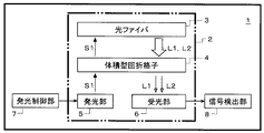
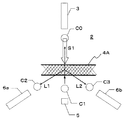
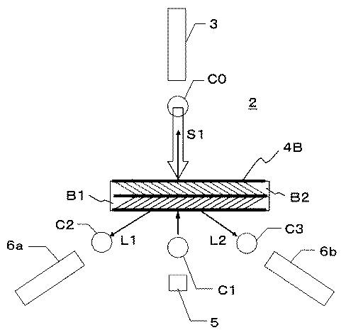
2 光通信用光学系
3 光ファイバ
4,4A,4B 体積型回折格子
4s 回折格子基板面
5 発光部(LD)
6,6a,6b 受光部(PD,光ファイバ)
7 発光制御部
8 信号検出部
C0〜C3 コリメータレンズ(ボールレンズ)
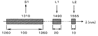
S1 短波長帯域の光束
L1,L2 長波長帯域の光束
Claims (6)
- 離散的に異なる複数の波長帯域を分岐・結合する光通信用光学系であって、2種類以上の周期的な屈折率変調により複数の回折を行う体積型回折格子を有し、その屈折率変調の方向がいずれも回折格子基板面の法線に対して垂直ではなく、前記複数の波長帯域における任意の光線の波長について、短波長帯域の光が前記体積型回折格子を非回折で透過し、複数の長波長帯域の光が前記体積型回折格子で回折され、前記体積型回折格子に対する各波長帯域の入射光及び短波長帯域の透過光が回折格子基板面に対して垂直又は略垂直であり、前記屈折率変調の方向がいずれも回折格子基板面の法線に対して60°〜80°であり、いずれの屈折率変調についても以下の条件式(1)を満足することを特徴とする光通信用光学系;
10000<h/(Δn・Λ)<15000 …(1)
ただし、
h:体積型回折格子の基板厚み、
Λ:体積型回折格子の屈折率変調の周期、
Δn:体積型回折格子の屈折率変調量、
である。 - さらに、長波長帯域の光を射出する光ファイバと、短波長帯域の光を射出する発光部と、複数の異なる長波長帯域の光に対応した受光部と、を有し、前記体積型回折格子が、前記光ファイバからの射出光を複数の異なる長波長帯域の光に分岐して前記受光部に入射させ、前記発光部からの射出光を前記光ファイバに入射させることを特徴とする請求項1記載の光通信用光学系。
- さらに、前記光ファイバからの射出光をコリメートし、かつ、前記体積型回折格子を非回折で透過した射出光を前記光ファイバの端面で結像させるコリメータレンズを有することを特徴とする請求項2記載の光通信用光学系。
- 前記体積型回折格子が、フィルムを積層し圧延することにより構成されていることを特徴とする請求項1〜3のいずれか1項に記載の光通信用光学系。
- 前記体積型回折格子が、塗布により形成されるフィルムの積層により構成されていることを特徴とする請求項1〜3のいずれか1項に記載の光通信用光学系。
- 請求項1〜5のいずれか1項に記載の光通信用光学系を備えたことを特徴とする光通信装置。
Priority Applications (1)
| Application Number | Priority Date | Filing Date | Title |
|---|---|---|---|
| JP2006152713A JP5145656B2 (ja) | 2006-05-31 | 2006-05-31 | 光通信用光学系及び光通信装置 |
Applications Claiming Priority (1)
| Application Number | Priority Date | Filing Date | Title |
|---|---|---|---|
| JP2006152713A JP5145656B2 (ja) | 2006-05-31 | 2006-05-31 | 光通信用光学系及び光通信装置 |
Publications (2)
| Publication Number | Publication Date |
|---|---|
| JP2007322739A JP2007322739A (ja) | 2007-12-13 |
| JP5145656B2 true JP5145656B2 (ja) | 2013-02-20 |
Family
ID=38855604
Family Applications (1)
| Application Number | Title | Priority Date | Filing Date |
|---|---|---|---|
| JP2006152713A Expired - Fee Related JP5145656B2 (ja) | 2006-05-31 | 2006-05-31 | 光通信用光学系及び光通信装置 |
Country Status (1)
| Country | Link |
|---|---|
| JP (1) | JP5145656B2 (ja) |
Family Cites Families (10)
| Publication number | Priority date | Publication date | Assignee | Title |
|---|---|---|---|---|
| JPS5342043A (en) * | 1976-09-28 | 1978-04-17 | Nec Corp | Optical multichannel system |
| JPS5455456A (en) * | 1977-10-12 | 1979-05-02 | Canon Inc | Method of composing and separating plural beams |
| JPS61221723A (ja) * | 1985-10-25 | 1986-10-02 | Canon Inc | 複数ビ−ムの合成方法 |
| JPS6236628A (ja) * | 1986-07-26 | 1987-02-17 | Canon Inc | 複数ビ−ムの合成方法 |
| JP3157852B2 (ja) * | 1991-06-12 | 2001-04-16 | シャープ株式会社 | 単方向光伝送モジュール |
| JPH05288910A (ja) * | 1992-04-14 | 1993-11-05 | Dainippon Printing Co Ltd | 回折格子 |
| JPH07104154A (ja) * | 1993-10-07 | 1995-04-21 | Hitachi Ltd | 光伝送モジュールおよび光伝送装置 |
| JPH07281015A (ja) * | 1994-04-08 | 1995-10-27 | Hideo Shingu | 積層型光学格子の作製方法 |
| JP2003322764A (ja) * | 2002-04-30 | 2003-11-14 | Alps Electric Co Ltd | 光通信モジュール |
| JP2005275060A (ja) * | 2004-03-25 | 2005-10-06 | Konica Minolta Holdings Inc | 光学素子及び光通信モジュール |
-
2006
- 2006-05-31 JP JP2006152713A patent/JP5145656B2/ja not_active Expired - Fee Related
Also Published As
| Publication number | Publication date |
|---|---|
| JP2007322739A (ja) | 2007-12-13 |
Similar Documents
| Publication | Publication Date | Title |
|---|---|---|
| US20190173585A1 (en) | Optical mode matching | |
| CN103999303B (zh) | 集成亚波长光栅系统 | |
| US9485046B1 (en) | Optical spot array pitch compressor | |
| US20100290128A1 (en) | Optical module | |
| KR20110113161A (ko) | 광학적 파장분할다중 방식 광통신모듈 | |
| US6999663B2 (en) | Fiber optic tap | |
| US6724533B2 (en) | Lamellar grating structure with polarization-independent diffraction efficiency | |
| WO2001095540A2 (en) | Device and method for optical performance monitoring in an optical communications network | |
| US6829096B1 (en) | Bi-directional wavelength division multiplexing/demultiplexing devices | |
| JPH11223745A (ja) | 波長多重(wdm)光を分波するための波長分波器と組み合せたバーチャル・イメージ・フェーズ・アレイ(vipa)を備える装置 | |
| US7403681B2 (en) | Wavelength selective optical device and method of tuning wavelength characteristics | |
| JP5145656B2 (ja) | 光通信用光学系及び光通信装置 | |
| JP4505313B2 (ja) | 光装置および光制御方法 | |
| JP2000131542A (ja) | 光送受信モジュール | |
| JPS6046682B2 (ja) | 光ビ−ム用光波多重分波回路 | |
| JP2003066269A (ja) | 波長多重分離光学デバイス及び波長多重光伝送モジュール | |
| US20040156596A1 (en) | Fiber optic tap with compensated spectral filter | |
| US20040201892A1 (en) | Diffraction grating element, optical module and optical communications system | |
| JP2002169054A (ja) | 波長合分波器 | |
| JP3933062B2 (ja) | 波長多重分波器 | |
| JP2010060653A (ja) | 光デバイスおよび光信号選択方法 | |
| JP4816258B2 (ja) | 表面反射回折格子を備えた光学装置 | |
| JP4696521B2 (ja) | デマルチプレクサ、光導波路、及び波長多重光伝送モジュール | |
| JPS58106516A (ja) | 光分波器 | |
| JP2008242450A (ja) | 光合分波器およびそれを用いた光送受信器 |
Legal Events
| Date | Code | Title | Description |
|---|---|---|---|
| A621 | Written request for application examination |
Free format text: JAPANESE INTERMEDIATE CODE: A621 Effective date: 20090428 |
|
| RD03 | Notification of appointment of power of attorney |
Free format text: JAPANESE INTERMEDIATE CODE: A7423 Effective date: 20120425 |
|
| A131 | Notification of reasons for refusal |
Free format text: JAPANESE INTERMEDIATE CODE: A131 Effective date: 20120703 |
|
| A521 | Written amendment |
Free format text: JAPANESE INTERMEDIATE CODE: A523 Effective date: 20120830 |
|
| TRDD | Decision of grant or rejection written | ||
| A01 | Written decision to grant a patent or to grant a registration (utility model) |
Free format text: JAPANESE INTERMEDIATE CODE: A01 Effective date: 20121030 |
|
| A61 | First payment of annual fees (during grant procedure) |
Free format text: JAPANESE INTERMEDIATE CODE: A61 Effective date: 20121112 |
|
| R150 | Certificate of patent (=grant) or registration of utility model |
Free format text: JAPANESE INTERMEDIATE CODE: R150 |
|
| FPAY | Renewal fee payment (prs date is renewal date of database) |
Free format text: PAYMENT UNTIL: 20151207 Year of fee payment: 3 |
|
| S533 | Written request for registration of change of name |
Free format text: JAPANESE INTERMEDIATE CODE: R313533 |
|
| R350 | Written notification of registration of transfer |
Free format text: JAPANESE INTERMEDIATE CODE: R350 |
|
| LAPS | Cancellation because of no payment of annual fees |