JP5075337B2 - 半導体基板をプラズマエッチングしてマスクを作るための装置 - Google Patents
半導体基板をプラズマエッチングしてマスクを作るための装置 Download PDFInfo
- Publication number
- JP5075337B2 JP5075337B2 JP2005371907A JP2005371907A JP5075337B2 JP 5075337 B2 JP5075337 B2 JP 5075337B2 JP 2005371907 A JP2005371907 A JP 2005371907A JP 2005371907 A JP2005371907 A JP 2005371907A JP 5075337 B2 JP5075337 B2 JP 5075337B2
- Authority
- JP
- Japan
- Prior art keywords
- shielding plate
- etched
- substrate
- pattern
- distance
- Prior art date
- Legal status (The legal status is an assumption and is not a legal conclusion. Google has not performed a legal analysis and makes no representation as to the accuracy of the status listed.)
- Expired - Fee Related
Links
Images


Classifications
-
- G—PHYSICS
- G03—PHOTOGRAPHY; CINEMATOGRAPHY; ANALOGOUS TECHNIQUES USING WAVES OTHER THAN OPTICAL WAVES; ELECTROGRAPHY; HOLOGRAPHY
- G03F—PHOTOMECHANICAL PRODUCTION OF TEXTURED OR PATTERNED SURFACES, e.g. FOR PRINTING, FOR PROCESSING OF SEMICONDUCTOR DEVICES; MATERIALS THEREFOR; ORIGINALS THEREFOR; APPARATUS SPECIALLY ADAPTED THEREFOR
- G03F1/00—Originals for photomechanical production of textured or patterned surfaces, e.g., masks, photo-masks, reticles; Mask blanks or pellicles therefor; Containers specially adapted therefor; Preparation thereof
- G03F1/20—Masks or mask blanks for imaging by charged particle beam [CPB] radiation, e.g. by electron beam; Preparation thereof
Landscapes
- Physics & Mathematics (AREA)
- General Physics & Mathematics (AREA)
- Electron Beam Exposure (AREA)
- Drying Of Semiconductors (AREA)
- Preparing Plates And Mask In Photomechanical Process (AREA)
Description
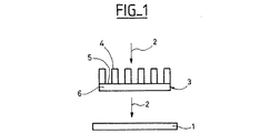
2 電子ビーム
3 透過マスク
4 突出部分
6 薄い膜
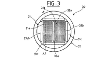
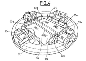
30 装置
31c エッチングされない領域
31a、31b エッチングされたパターンの領域
33a、33b、33c、33d、33e 遮蔽板
32 基板を保持するシステム
34 パターン領域の境界
dh 境界から距離
dv エッチングされない領域からの距離
Claims (13)
- 半導体基板をプラズマエッチングしてマスクを作るための装置であって、
エッチングされるべきでない少なくとも1つの領域を保護し、かつエッチングされるべきパターンを含んだ少なくとも1つの領域を露出するマスクで、部分的に覆われた半導体基板と、
前記基板の支持体と、
前記基板の方に向かうイオンの流れの形をしたプラズマを生成する手段と、
少なくとも1つの分離した導電性材料の遮蔽板とを備え、導電性材料の遮蔽板が、エッチングされるべき前記少なくとも1つのパターン領域とエッチングされるべきでない前記領域との間の境界に沿って、基板から一定の垂直距離離れたところに、導電性材料の遮蔽板と基板表面との間にギャップを残して、かつ前記境界の外側の一定の水平距離離れたところに、前記基板の上に配置され、かつ四辺形の形をしたエッチングされるべき前記少なくとも1つのパターン領域の各々の辺に対して平行な垂直板の形をとる、装置。 - 前記遮蔽板が、エッチングされるべきパターン領域の境界から一定距離離れたところにある、請求項1に記載の装置。
- 前記遮蔽板が、エッチングされるべき前記パターン領域の境界の外側に一定水平距離のところにある、請求項2に記載の装置。
- 前記遮蔽板が、前記基板から一定垂直距離離れたところにある、請求項2に記載の装置。
- 前記一定距離が、10mmよりも小さい、請求項2に記載の装置。
- 前記遮蔽板の高さが、5mmから20mmまでである、請求項1に記載の装置。
- 前記基板が、エッチングされるべきでない領域によって互いに分離された、エッチングされるべきパターンを含んだ複数の領域を含む、請求項1に記載の装置。
- 前記遮蔽板は、前記四辺形の角がエッチングされるべき他のパターン領域から前記一定距離以下のある距離離れたところにある場合、前記四辺形の角で途切れている、請求項7に記載の装置。
- 前記遮蔽板は、前記四辺形の角が他の導電性部分から前記一定距離以下のある距離離れたところにある場合、前記四辺形の角で途切れている、請求項1に記載の装置。
- 前記遮蔽板が金属である、請求項1に記載の装置。
- 前記遮蔽板がアルミニウムである、請求項10に記載の装置。
- 各遮蔽板がエッチングされるべき前記パターン領域の各々を包囲している、請求項7に記載の装置。
- 前記導電材料の遮蔽板が、前記支持体に取り付けられている、請求項1に記載の装置。
Applications Claiming Priority (2)
| Application Number | Priority Date | Filing Date | Title |
|---|---|---|---|
| FR0550002 | 2005-01-03 | ||
| FR0550002A FR2880469B1 (fr) | 2005-01-03 | 2005-01-03 | Dispositif de fabrication d'un masque par gravure par plasma d'un substrat semiconducteur |
Publications (2)
| Publication Number | Publication Date |
|---|---|
| JP2006191043A JP2006191043A (ja) | 2006-07-20 |
| JP5075337B2 true JP5075337B2 (ja) | 2012-11-21 |
Family
ID=34953717
Family Applications (1)
| Application Number | Title | Priority Date | Filing Date |
|---|---|---|---|
| JP2005371907A Expired - Fee Related JP5075337B2 (ja) | 2005-01-03 | 2005-12-26 | 半導体基板をプラズマエッチングしてマスクを作るための装置 |
Country Status (5)
| Country | Link |
|---|---|
| US (1) | US7938907B2 (ja) |
| EP (1) | EP1677146B1 (ja) |
| JP (1) | JP5075337B2 (ja) |
| CN (1) | CN100382250C (ja) |
| FR (1) | FR2880469B1 (ja) |
Families Citing this family (1)
| Publication number | Priority date | Publication date | Assignee | Title |
|---|---|---|---|---|
| KR101084268B1 (ko) * | 2009-09-25 | 2011-11-16 | 삼성모바일디스플레이주식회사 | 기판 센터링 장치 및 이를 구비한 유기물 증착 시스템 |
Family Cites Families (14)
| Publication number | Priority date | Publication date | Assignee | Title |
|---|---|---|---|---|
| US3887421A (en) * | 1973-01-22 | 1975-06-03 | Gen Motors Corp | Method of masking semiconductor wafers using a self-aligning mask |
| JPS63151948A (ja) * | 1986-12-15 | 1988-06-24 | Nec Corp | 露光用マスク |
| DE4241045C1 (de) | 1992-12-05 | 1994-05-26 | Bosch Gmbh Robert | Verfahren zum anisotropen Ätzen von Silicium |
| US5891348A (en) * | 1996-01-26 | 1999-04-06 | Applied Materials, Inc. | Process gas focusing apparatus and method |
| JPH09246251A (ja) * | 1996-03-01 | 1997-09-19 | Sony Corp | 半導体製造装置及び半導体製造方法 |
| JPH1174252A (ja) * | 1997-08-28 | 1999-03-16 | Sony Corp | 半導体装置および製造方法 |
| US6383938B2 (en) * | 1999-04-21 | 2002-05-07 | Alcatel | Method of anisotropic etching of substrates |
| JP2000340492A (ja) | 1999-05-28 | 2000-12-08 | Nec Corp | 電子線露光用マスクとそれを用いた半導体装置製造方法 |
| JP2001007013A (ja) * | 1999-06-24 | 2001-01-12 | Nikon Corp | 転写マスクブランクス及びその製造方法 |
| JP2002299226A (ja) * | 2001-04-03 | 2002-10-11 | Nikon Corp | 電子線露光用ステンシルマスク及びその作製方法 |
| JP2002329711A (ja) * | 2001-05-01 | 2002-11-15 | Matsushita Electric Ind Co Ltd | 平行平板型電極プラズマ処理装置 |
| FR2834382B1 (fr) * | 2002-01-03 | 2005-03-18 | Cit Alcatel | Procede et dispositif de gravure anisotrope du silicium a haut facteur d'aspect |
| JP2003273002A (ja) * | 2002-03-14 | 2003-09-26 | Sony Corp | マスクの製造方法 |
| US6960263B2 (en) * | 2002-04-25 | 2005-11-01 | Applied Materials, Inc. | Shadow frame with cross beam for semiconductor equipment |
-
2005
- 2005-01-03 FR FR0550002A patent/FR2880469B1/fr not_active Expired - Fee Related
- 2005-12-21 EP EP05112633A patent/EP1677146B1/fr active Active
- 2005-12-26 JP JP2005371907A patent/JP5075337B2/ja not_active Expired - Fee Related
- 2005-12-29 US US11/319,630 patent/US7938907B2/en active Active
-
2006
- 2006-01-04 CN CNB2006100003062A patent/CN100382250C/zh active Active
Also Published As
| Publication number | Publication date |
|---|---|
| FR2880469B1 (fr) | 2007-04-27 |
| US20060148274A1 (en) | 2006-07-06 |
| JP2006191043A (ja) | 2006-07-20 |
| CN100382250C (zh) | 2008-04-16 |
| US7938907B2 (en) | 2011-05-10 |
| EP1677146A3 (fr) | 2007-03-28 |
| CN1801462A (zh) | 2006-07-12 |
| EP1677146A2 (fr) | 2006-07-05 |
| FR2880469A1 (fr) | 2006-07-07 |
| EP1677146B1 (fr) | 2012-09-19 |
Similar Documents
| Publication | Publication Date | Title |
|---|---|---|
| JP2009200510A (ja) | リソグラフィックテンプレート | |
| JP2002252157A (ja) | マスク作製用部材およびその製造方法ならびにマスクおよびその製造方法ならびに露光方法ならびに半導体装置の製造方法 | |
| KR100845347B1 (ko) | 복합 패터닝 방법 및 장치 | |
| CN107799402A (zh) | 二次图形的形成方法 | |
| JP2000114168A (ja) | 荷電粒子線マスクとその製造方法と荷電粒子線リソグラフィシステムの操作方法 | |
| JP2006527398A (ja) | レチクルを設計し、半導体素子をレチクルで作製する方法 | |
| JP2000331928A (ja) | リソグラフ方法 | |
| US6361911B1 (en) | Using a dummy frame pattern to improve CD control of VSB E-beam exposure system and the proximity effect of laser beam exposure system and Gaussian E-beam exposure system | |
| KR101599097B1 (ko) | 광학 리소그래피 장치 | |
| US11150561B2 (en) | Method and apparatus for collecting information used in image-error compensation | |
| JP2001312045A (ja) | マスクの形成方法 | |
| US4349621A (en) | Process for X-ray microlithography using thin film eutectic masks | |
| JP4804802B2 (ja) | フォトマスク及びこれを用いたパターン製造方法 | |
| JP5075337B2 (ja) | 半導体基板をプラズマエッチングしてマスクを作るための装置 | |
| TWI740960B (zh) | 遠紫外線對準標記的形成方法及具有對準標記的罩幕 | |
| TW518663B (en) | Electron beam projection mask | |
| JP2010074043A (ja) | 半導体製造方法および半導体製造装置 | |
| JP2004111713A (ja) | 露光用マスク、露光方法、半導体装置の製造方法および露光用マスクの製造方法 | |
| JP5223197B2 (ja) | パターン測定方法及び、フォトマスクの検査方法 | |
| JPH11168049A (ja) | ステンシルマスクの製造方法 | |
| JP2000047367A (ja) | マイクロリソグラフィ製造におけるパタ―ン形成を改善する方法およびシステム | |
| JPH0844039A (ja) | ハーフトーン方式位相シフトマスク及びレジスト露光方法 | |
| Wynand et al. | Photolithography Enhancements | |
| KR100230377B1 (ko) | 요철부가 있는 정렬키를 갖는 포토마스크 | |
| JP2005259840A (ja) | 露光方法、露光用マスク及び描画方法 |
Legal Events
| Date | Code | Title | Description |
|---|---|---|---|
| A621 | Written request for application examination |
Free format text: JAPANESE INTERMEDIATE CODE: A621 Effective date: 20081219 |
|
| A977 | Report on retrieval |
Free format text: JAPANESE INTERMEDIATE CODE: A971007 Effective date: 20110517 |
|
| A131 | Notification of reasons for refusal |
Free format text: JAPANESE INTERMEDIATE CODE: A131 Effective date: 20110524 |
|
| A601 | Written request for extension of time |
Free format text: JAPANESE INTERMEDIATE CODE: A601 Effective date: 20110822 |
|
| A602 | Written permission of extension of time |
Free format text: JAPANESE INTERMEDIATE CODE: A602 Effective date: 20110825 |
|
| A521 | Written amendment |
Free format text: JAPANESE INTERMEDIATE CODE: A523 Effective date: 20111118 |
|
| A131 | Notification of reasons for refusal |
Free format text: JAPANESE INTERMEDIATE CODE: A131 Effective date: 20111206 |
|
| A521 | Written amendment |
Free format text: JAPANESE INTERMEDIATE CODE: A523 Effective date: 20120119 |
|
| TRDD | Decision of grant or rejection written | ||
| A01 | Written decision to grant a patent or to grant a registration (utility model) |
Free format text: JAPANESE INTERMEDIATE CODE: A01 Effective date: 20120821 |
|
| A01 | Written decision to grant a patent or to grant a registration (utility model) |
Free format text: JAPANESE INTERMEDIATE CODE: A01 |
|
| A61 | First payment of annual fees (during grant procedure) |
Free format text: JAPANESE INTERMEDIATE CODE: A61 Effective date: 20120827 |
|
| R150 | Certificate of patent or registration of utility model |
Free format text: JAPANESE INTERMEDIATE CODE: R150 |
|
| FPAY | Renewal fee payment (event date is renewal date of database) |
Free format text: PAYMENT UNTIL: 20150831 Year of fee payment: 3 |
|
| R250 | Receipt of annual fees |
Free format text: JAPANESE INTERMEDIATE CODE: R250 |
|
| R250 | Receipt of annual fees |
Free format text: JAPANESE INTERMEDIATE CODE: R250 |
|
| LAPS | Cancellation because of no payment of annual fees |