JP5020650B2 - Vapor deposition apparatus, vapor deposition method, and vapor deposition apparatus manufacturing method - Google Patents
Vapor deposition apparatus, vapor deposition method, and vapor deposition apparatus manufacturing method Download PDFInfo
- Publication number
- JP5020650B2 JP5020650B2 JP2007023402A JP2007023402A JP5020650B2 JP 5020650 B2 JP5020650 B2 JP 5020650B2 JP 2007023402 A JP2007023402 A JP 2007023402A JP 2007023402 A JP2007023402 A JP 2007023402A JP 5020650 B2 JP5020650 B2 JP 5020650B2
- Authority
- JP
- Japan
- Prior art keywords
- film
- vapor deposition
- partition
- blowing
- forming material
- Prior art date
- Legal status (The legal status is an assumption and is not a legal conclusion. Google has not performed a legal analysis and makes no representation as to the accuracy of the status listed.)
- Expired - Fee Related
Links
- 238000007740 vapor deposition Methods 0.000 title claims description 111
- 238000000034 method Methods 0.000 title claims description 26
- 238000004519 manufacturing process Methods 0.000 title description 9
- 238000007664 blowing Methods 0.000 claims description 109
- 238000005192 partition Methods 0.000 claims description 105
- 230000007246 mechanism Effects 0.000 claims description 97
- 239000000463 material Substances 0.000 claims description 83
- 238000000151 deposition Methods 0.000 claims description 18
- 230000008021 deposition Effects 0.000 claims description 16
- 229910052751 metal Inorganic materials 0.000 claims description 9
- 239000002184 metal Substances 0.000 claims description 9
- 238000001704 evaporation Methods 0.000 claims description 4
- 230000008016 vaporization Effects 0.000 claims description 4
- 230000008020 evaporation Effects 0.000 claims description 3
- 239000011368 organic material Substances 0.000 claims description 3
- 238000000638 solvent extraction Methods 0.000 claims description 3
- 239000010408 film Substances 0.000 description 127
- 239000000758 substrate Substances 0.000 description 86
- 239000007789 gas Substances 0.000 description 21
- 239000010410 layer Substances 0.000 description 20
- 230000015572 biosynthetic process Effects 0.000 description 16
- 238000002474 experimental method Methods 0.000 description 16
- 230000008569 process Effects 0.000 description 12
- 238000012864 cross contamination Methods 0.000 description 11
- 238000009751 slip forming Methods 0.000 description 8
- 238000003380 quartz crystal microbalance Methods 0.000 description 6
- 239000000356 contaminant Substances 0.000 description 5
- XKRFYHLGVUSROY-UHFFFAOYSA-N Argon Chemical compound [Ar] XKRFYHLGVUSROY-UHFFFAOYSA-N 0.000 description 4
- 230000008859 change Effects 0.000 description 4
- 239000013078 crystal Substances 0.000 description 4
- 238000005516 engineering process Methods 0.000 description 4
- 239000010409 thin film Substances 0.000 description 4
- 238000011109 contamination Methods 0.000 description 3
- 238000009792 diffusion process Methods 0.000 description 3
- 239000011521 glass Substances 0.000 description 3
- 239000007788 liquid Substances 0.000 description 3
- 239000000126 substance Substances 0.000 description 3
- 229910052786 argon Inorganic materials 0.000 description 2
- 230000004888 barrier function Effects 0.000 description 2
- 239000012159 carrier gas Substances 0.000 description 2
- 230000005525 hole transport Effects 0.000 description 2
- 239000011261 inert gas Substances 0.000 description 2
- IBHBKWKFFTZAHE-UHFFFAOYSA-N n-[4-[4-(n-naphthalen-1-ylanilino)phenyl]phenyl]-n-phenylnaphthalen-1-amine Chemical compound C1=CC=CC=C1N(C=1C2=CC=CC=C2C=CC=1)C1=CC=C(C=2C=CC(=CC=2)N(C=2C=CC=CC=2)C=2C3=CC=CC=C3C=CC=2)C=C1 IBHBKWKFFTZAHE-UHFFFAOYSA-N 0.000 description 2
- 239000012044 organic layer Substances 0.000 description 2
- 239000010453 quartz Substances 0.000 description 2
- 239000002994 raw material Substances 0.000 description 2
- VYPSYNLAJGMNEJ-UHFFFAOYSA-N silicon dioxide Inorganic materials O=[Si]=O VYPSYNLAJGMNEJ-UHFFFAOYSA-N 0.000 description 2
- 239000007787 solid Substances 0.000 description 2
- 230000007723 transport mechanism Effects 0.000 description 2
- 239000005725 8-Hydroxyquinoline Substances 0.000 description 1
- XUIMIQQOPSSXEZ-UHFFFAOYSA-N Silicon Chemical compound [Si] XUIMIQQOPSSXEZ-UHFFFAOYSA-N 0.000 description 1
- 238000005229 chemical vapour deposition Methods 0.000 description 1
- 239000000470 constituent Substances 0.000 description 1
- 230000005281 excited state Effects 0.000 description 1
- 230000005283 ground state Effects 0.000 description 1
- 229910052738 indium Inorganic materials 0.000 description 1
- APFVFJFRJDLVQX-UHFFFAOYSA-N indium atom Chemical compound [In] APFVFJFRJDLVQX-UHFFFAOYSA-N 0.000 description 1
- AMGQUBHHOARCQH-UHFFFAOYSA-N indium;oxotin Chemical compound [In].[Sn]=O AMGQUBHHOARCQH-UHFFFAOYSA-N 0.000 description 1
- 230000001678 irradiating effect Effects 0.000 description 1
- 230000009191 jumping Effects 0.000 description 1
- 239000004973 liquid crystal related substance Substances 0.000 description 1
- 239000012528 membrane Substances 0.000 description 1
- 238000002156 mixing Methods 0.000 description 1
- 239000000203 mixture Substances 0.000 description 1
- 238000012986 modification Methods 0.000 description 1
- 230000004048 modification Effects 0.000 description 1
- 230000003287 optical effect Effects 0.000 description 1
- 229960003540 oxyquinoline Drugs 0.000 description 1
- 230000036632 reaction speed Effects 0.000 description 1
- 229910052710 silicon Inorganic materials 0.000 description 1
- 239000010703 silicon Substances 0.000 description 1
- 239000002356 single layer Substances 0.000 description 1
- 230000003595 spectral effect Effects 0.000 description 1
- 238000000859 sublimation Methods 0.000 description 1
- 230000008022 sublimation Effects 0.000 description 1
- XOLBLPGZBRYERU-UHFFFAOYSA-N tin dioxide Chemical compound O=[Sn]=O XOLBLPGZBRYERU-UHFFFAOYSA-N 0.000 description 1
- 229910001887 tin oxide Inorganic materials 0.000 description 1
- 238000009834 vaporization Methods 0.000 description 1
Images


Classifications
-
- H—ELECTRICITY
- H10—SEMICONDUCTOR DEVICES; ELECTRIC SOLID-STATE DEVICES NOT OTHERWISE PROVIDED FOR
- H10K—ORGANIC ELECTRIC SOLID-STATE DEVICES
- H10K50/00—Organic light-emitting devices
- H10K50/10—OLEDs or polymer light-emitting diodes [PLED]
- H10K50/11—OLEDs or polymer light-emitting diodes [PLED] characterised by the electroluminescent [EL] layers
-
- C—CHEMISTRY; METALLURGY
- C23—COATING METALLIC MATERIAL; COATING MATERIAL WITH METALLIC MATERIAL; CHEMICAL SURFACE TREATMENT; DIFFUSION TREATMENT OF METALLIC MATERIAL; COATING BY VACUUM EVAPORATION, BY SPUTTERING, BY ION IMPLANTATION OR BY CHEMICAL VAPOUR DEPOSITION, IN GENERAL; INHIBITING CORROSION OF METALLIC MATERIAL OR INCRUSTATION IN GENERAL
- C23C—COATING METALLIC MATERIAL; COATING MATERIAL WITH METALLIC MATERIAL; SURFACE TREATMENT OF METALLIC MATERIAL BY DIFFUSION INTO THE SURFACE, BY CHEMICAL CONVERSION OR SUBSTITUTION; COATING BY VACUUM EVAPORATION, BY SPUTTERING, BY ION IMPLANTATION OR BY CHEMICAL VAPOUR DEPOSITION, IN GENERAL
- C23C14/00—Coating by vacuum evaporation, by sputtering or by ion implantation of the coating forming material
- C23C14/22—Coating by vacuum evaporation, by sputtering or by ion implantation of the coating forming material characterised by the process of coating
-
- B—PERFORMING OPERATIONS; TRANSPORTING
- B01—PHYSICAL OR CHEMICAL PROCESSES OR APPARATUS IN GENERAL
- B01B—BOILING; BOILING APPARATUS ; EVAPORATION; EVAPORATION APPARATUS
- B01B1/00—Boiling; Boiling apparatus for physical or chemical purposes ; Evaporation in general
- B01B1/005—Evaporation for physical or chemical purposes; Evaporation apparatus therefor, e.g. evaporation of liquids for gas phase reactions
-
- C—CHEMISTRY; METALLURGY
- C23—COATING METALLIC MATERIAL; COATING MATERIAL WITH METALLIC MATERIAL; CHEMICAL SURFACE TREATMENT; DIFFUSION TREATMENT OF METALLIC MATERIAL; COATING BY VACUUM EVAPORATION, BY SPUTTERING, BY ION IMPLANTATION OR BY CHEMICAL VAPOUR DEPOSITION, IN GENERAL; INHIBITING CORROSION OF METALLIC MATERIAL OR INCRUSTATION IN GENERAL
- C23C—COATING METALLIC MATERIAL; COATING MATERIAL WITH METALLIC MATERIAL; SURFACE TREATMENT OF METALLIC MATERIAL BY DIFFUSION INTO THE SURFACE, BY CHEMICAL CONVERSION OR SUBSTITUTION; COATING BY VACUUM EVAPORATION, BY SPUTTERING, BY ION IMPLANTATION OR BY CHEMICAL VAPOUR DEPOSITION, IN GENERAL
- C23C14/00—Coating by vacuum evaporation, by sputtering or by ion implantation of the coating forming material
- C23C14/22—Coating by vacuum evaporation, by sputtering or by ion implantation of the coating forming material characterised by the process of coating
- C23C14/56—Apparatus specially adapted for continuous coating; Arrangements for maintaining the vacuum, e.g. vacuum locks
- C23C14/562—Apparatus specially adapted for continuous coating; Arrangements for maintaining the vacuum, e.g. vacuum locks for coating elongated substrates
-
- H—ELECTRICITY
- H01—ELECTRIC ELEMENTS
- H01L—SEMICONDUCTOR DEVICES NOT COVERED BY CLASS H10
- H01L21/00—Processes or apparatus adapted for the manufacture or treatment of semiconductor or solid state devices or of parts thereof
- H01L21/02—Manufacture or treatment of semiconductor devices or of parts thereof
- H01L21/02104—Forming layers
- H01L21/02107—Forming insulating materials on a substrate
- H01L21/02225—Forming insulating materials on a substrate characterised by the process for the formation of the insulating layer
- H01L21/0226—Forming insulating materials on a substrate characterised by the process for the formation of the insulating layer formation by a deposition process
- H01L21/02263—Forming insulating materials on a substrate characterised by the process for the formation of the insulating layer formation by a deposition process deposition from the gas or vapour phase
-
- H—ELECTRICITY
- H10—SEMICONDUCTOR DEVICES; ELECTRIC SOLID-STATE DEVICES NOT OTHERWISE PROVIDED FOR
- H10K—ORGANIC ELECTRIC SOLID-STATE DEVICES
- H10K2102/00—Constructional details relating to the organic devices covered by this subclass
- H10K2102/301—Details of OLEDs
- H10K2102/351—Thickness
Landscapes
- Chemical & Material Sciences (AREA)
- Chemical Kinetics & Catalysis (AREA)
- Engineering & Computer Science (AREA)
- Materials Engineering (AREA)
- Mechanical Engineering (AREA)
- Metallurgy (AREA)
- Organic Chemistry (AREA)
- Physics & Mathematics (AREA)
- Condensed Matter Physics & Semiconductors (AREA)
- General Physics & Mathematics (AREA)
- Manufacturing & Machinery (AREA)
- Computer Hardware Design (AREA)
- Microelectronics & Electronic Packaging (AREA)
- Power Engineering (AREA)
- Optics & Photonics (AREA)
- Physical Vapour Deposition (AREA)
- Electroluminescent Light Sources (AREA)
Description
本発明は、蒸着装置、蒸着方法および蒸着装置の製造方法に関する。特に、蒸着装置内部のコンタミネーションに関する。 The present invention relates to a vapor deposition apparatus, a vapor deposition method, and a method for manufacturing the vapor deposition apparatus. In particular, it relates to contamination inside the vapor deposition apparatus.
フラットパネルディスプレイなどの電子機器を製造する際、所定の成膜材料を気化させて、これにより生成された気体分子を被処理体に付着させることによって、被処理体を成膜する蒸着法が広く用いられている。このような技術を用いて製造した機器のうち、特に、有機ELディスプレイは、自発光し、反応速度が早く、消費電力が少ない等の点において液晶ディスプレイより優れていると言われている。このため、今後、ますますの需要が見込まれるフラットパネルディスプレイの製造業界において、有機ELディスプレイへの注目度は高く、これに伴い、有機ELディスプレイを製造する際に用いられる上記技術も非常に重要になっている。 When manufacturing electronic devices such as flat panel displays, there is a wide range of vapor deposition methods for depositing a target object by vaporizing a predetermined film forming material and attaching gas molecules generated thereby to the target object. It is used. Among devices manufactured using such a technique, in particular, an organic EL display is said to be superior to a liquid crystal display in that it emits light, has a high reaction speed, and consumes less power. For this reason, in the manufacturing industry of flat panel displays, which are expected to be increasingly demanded in the future, attention to organic EL displays is high, and accordingly, the above-mentioned technology used for manufacturing organic EL displays is also very important. It has become.
このような社会的背景から注目が集まっている上記技術は、蒸着装置によって具現化されるが、従来の蒸着装置では、1つの処理容器内に1つの蒸着源が納められていた(たとえば、特許文献1を参照。)。よって、従来の蒸着装置では、蒸着源から放出される気化分子を、マスクに通すことにより被処理体の所定の位置に気化分子を付着させ、これにより、被処理体上に所望の成膜を施していた。このため、被処理体上に一層の膜を形成するのに1つの処理容器が必要であった。
The above-mentioned technique that has attracted attention from such a social background is embodied by a vapor deposition apparatus. However, in a conventional vapor deposition apparatus, one vapor deposition source is stored in one processing container (for example, patents). See
しかしながら、このように一層の膜を形成するために1つの処理容器が必要となると、複数層の膜を被処理体に形成するためには複数の処理容器が必要となり、フットプリントが大きくなる。この結果、工場の規模が大きくなるばかりでなく、被処理体を搬送中、その被処理体に汚染物が付着する可能性が高くなる。 However, when one processing container is required to form a single layer film as described above, a plurality of processing containers are required to form a plurality of layers of films on the object to be processed, and the footprint increases. As a result, not only the scale of the factory is increased, but also the possibility that contaminants adhere to the object to be processed is increased while the object is being transported.
一方、この問題を解消するために、1つの処理容器内に複数の蒸着源を配設し、各蒸着源により気化された成膜分子を被処理体に付着させることにより、被処理体上に連続的に複数の薄膜を形成することも考えられる。しかしながら、この場合には、隣り合う蒸着源から放出された成膜分子が、隣り合う蒸着源から放出された成膜分子に混入し合い(クロスコンタミネーション)、各層の膜質が悪くなる可能性がある。 On the other hand, in order to solve this problem, a plurality of vapor deposition sources are provided in one processing container, and film-forming molecules vaporized by the respective vapor deposition sources are attached to the object to be processed. It is also conceivable to form a plurality of thin films continuously. However, in this case, film forming molecules released from adjacent vapor deposition sources may mix with film forming molecules emitted from adjacent vapor deposition sources (cross-contamination), and the film quality of each layer may deteriorate. is there.
上記問題を解消するために、本発明では、クロスコンタミネーションを低減させながら、同一処理容器内にて複数層の膜を連続的に形成する蒸着装置、蒸着方法および蒸着装置の製造方法が提供される。 In order to solve the above problems, the present invention provides a vapor deposition apparatus, a vapor deposition method, and a vapor deposition apparatus manufacturing method for continuously forming a plurality of layers of films in the same processing vessel while reducing cross contamination. The
すなわち、上記課題を解決するために、本発明のある観点によれば、蒸着により処理容器内にて被処理体を成膜処理する蒸着装置であって、成膜材料を収納し、収納された成膜材料をそれぞれ気化させる複数の蒸着源と、前記複数の蒸着源にそれぞれ連結され、吹き出し口を有し、前記複数の蒸着源にて気化された成膜材料を前記吹き出し口からそれぞれ吹き出す複数の吹き出し機構と、前記複数の吹き出し機構のうち、隣り合う吹き出し機構の間に配置され、前記隣り合う吹き出し機構をそれぞれ仕切る1または2以上の隔壁と、を備えた蒸着装置が提供される。 That is, in order to solve the above-described problem, according to one aspect of the present invention, a vapor deposition apparatus that performs film deposition processing on an object to be processed in a processing container by vapor deposition, the film deposition material is stored and stored. A plurality of vapor deposition sources for vaporizing film forming materials, and a plurality of vapor deposition sources connected to the plurality of vapor deposition sources, each having a blow-out port, and a plurality of film-forming materials vaporized at the plurality of vapor deposition sources from the blow-out ports, respectively. There is provided a vapor deposition apparatus comprising: a plurality of blowing mechanisms; and one or two or more partition walls arranged between adjacent blowing mechanisms among the plurality of blowing mechanisms and partitioning the neighboring blowing mechanisms.
ここで、気化とは、液体が気体に変わる現象だけでなく、固体が液体の状態を経ずに直接気体に変わる現象(すなわち、昇華)も含んでいる。 Here, the vaporization includes not only a phenomenon in which a liquid turns into a gas but also a phenomenon in which a solid directly turns into a gas without going through a liquid state (that is, sublimation).
これによれば、複数の蒸着源にて気化された成膜材料(成膜分子)が、同一処理容器内に設けられた複数の吹き出し機構の吹き出し口からそれぞれ吹き出される。このとき、隣り合う吹き出し機構の間には、前記隣り合う吹き出し機構をそれぞれ仕切る1または2以上の隔壁が設けられている。これにより、各吹き出し口から吹き出された成膜材料が各隔壁を超えて隣の吹き出し口側へ飛来することを抑止しながら(すなわち、クロスコンタミネーションを抑止しながら)、気化された成膜材料により同一処理容器内にて被処理体に膜を連続的に形成することができる。これにより、隣り合う蒸着源から気化された成膜分子が、隣り合う蒸着源から気化された成膜分子に混入し(すなわち、クロスコンタミネーション)、各層の膜質を劣化させることを回避することができる。 According to this, the film-forming material (film-forming molecule) vaporized by the plurality of vapor deposition sources is blown out from the blow-out ports of the plurality of blow-out mechanisms provided in the same processing container. At this time, one or more partition walls are provided between the adjacent blowing mechanisms to partition the adjacent blowing mechanisms. As a result, the film forming material blown out from each outlet is prevented from flying over the respective partition walls to the adjacent outlet (that is, while suppressing cross-contamination) and vaporized film forming material. Thus, a film can be continuously formed on the object to be processed in the same processing container. Thereby, it is possible to avoid that the film forming molecules vaporized from the adjacent vapor deposition source are mixed into the film vaporized molecules vaporized from the adjacent vapor deposition source (that is, cross contamination) and the film quality of each layer is deteriorated. it can.
これに加えて、かかる構成によれば、同一処理容器内にて連続成膜するため、搬送中に被処理体に汚染物が付着することを低減することができる。この結果、クロスコンタミネーションを抑止することにより各層の特性を良好に保ちつつ、被処理体上に付着した汚染物の数を少なくすることによりエネルギー界面制御性を高くして、エネルギー障壁を低くすることができる。この結果、有機EL素子の発光強度(輝度)を向上させることができる。また、同一の処理容器内にて被処理体に連続成膜が施されることによりフットプリントを小さくすることができる。 In addition, according to this configuration, since the film is continuously formed in the same processing container, it is possible to reduce the adhesion of contaminants to the object to be processed during conveyance. As a result, it is possible to increase the energy interface controllability and reduce the energy barrier by reducing the number of contaminants adhering to the object to be processed while keeping the characteristics of each layer good by suppressing cross contamination. it can. As a result, the emission intensity (luminance) of the organic EL element can be improved. Moreover, a footprint can be made small by performing continuous film-forming on a to-be-processed object within the same processing container.
なお、各蒸着源に収納された成膜材料は、有機EL成膜材料または有機金属成膜材料であってもよく、前記蒸着装置は、有機EL成膜材料または有機金属成膜材料を有機材料として被処理体に有機EL膜または有機金属膜のいずれかを形成する装置であってもよい。 The film forming material stored in each vapor deposition source may be an organic EL film forming material or an organic metal film forming material, and the vapor deposition apparatus converts the organic EL film forming material or the organic metal film forming material into an organic material. As an apparatus, an organic EL film or an organic metal film may be formed on an object to be processed.
また、前記複数の吹き出し機構は、同一形状を有し、等間隔に平行して配置され、前記1または2以上の隔壁は、同一形状を有し、前記隣り合う吹き出し機構の間にて前記隣り合う吹き出し機構から等距離の位置に等間隔に平行して配置されていてもよい。 The plurality of blowing mechanisms have the same shape and are arranged in parallel at equal intervals, and the one or more partition walls have the same shape and are adjacent to each other between the neighboring blowing mechanisms. You may arrange | position in parallel at equal intervals in the position of equidistant from the matching blowing mechanism.
また、前記隣の吹き出し機構の面に対向する各隔壁の面は、前記隣の吹き出し機構の面より大きいほうがよい。これによれば、隔壁により各吹き出し機構の吹き出し口から吹き出された成膜材料が、隣の吹き出し機構側に飛来することを抑制することができる。 The surface of each partition wall facing the surface of the adjacent blowing mechanism should be larger than the surface of the adjacent blowing mechanism. According to this, it can suppress that the film-forming material blown out from the blower outlet of each blower mechanism by the partition fly to the next blower mechanism side.
さらに、前記1または2以上の隔壁を、前記隣り合う吹き出し機構に設けられた吹き出し口から放射状に拡散される成膜材料のうち、各隔壁に遮られずに直進しながら被処理体まで到達した最長飛距離の成膜材料の到達位置が、前記隣り合う吹き出し機構から等距離にある被処理体上の位置よりも前記最長飛距離の成膜材料が吹き出された吹き出し口側に位置し、かつ、前記成膜材料の最長飛距離は、前記成膜材料の平均自由工程よりも短いという2つの条件を満たすように配置してもよい。 Further, the one or two or more partition walls reach the object to be processed while straightly traveling without being blocked by each partition wall from among the film-forming materials that are diffused radially from the blowing ports provided in the adjacent blowing mechanisms. The position at which the film-forming material with the longest flight distance reaches is located closer to the outlet from which the film-forming material with the longest flight distance is blown out than the position on the target object that is equidistant from the adjacent blowing mechanism; The longest flight distance of the film forming material may be arranged so as to satisfy the two conditions of being shorter than the mean free path of the film forming material.
これによれば、上記2つの条件を満たすように、各隔壁の配置位置が特定される。1つ目の条件、すなわち、各隔壁に遮られずに直進しながら被処理体まで到達した最長飛距離の成膜材料の到達位置は、前記隣り合う吹き出し機構から等距離にある被処理体上の位置よりも前記最長飛距離の成膜材料が吹き出された吹き出し口側に位置するという条件が満たされることにより、隣の吹き出し口から吹き出される成膜分子中に混入するコンタミネーションはほとんどなくなる。これにより、各吹き出し口から吹き出された成膜分子のみから所望の特性の膜を被処理体上に連続的に形成することができる。 According to this, the arrangement position of each partition is specified so as to satisfy the above two conditions. The first condition, that is, the arrival position of the film-forming material with the longest flight distance that has reached the object to be processed while traveling straight without being blocked by each partition, is on the object to be processed that is equidistant from the adjacent blowing mechanism. By satisfying the condition that the film-forming material having the longest flight distance is located on the side of the blow-out port from which the film is blown, there is almost no contamination mixed in the film-forming molecules blown out from the next blow-out port. . Thus, a film having desired characteristics can be continuously formed on the object to be processed only from the film forming molecules blown out from the respective outlets.
また、2つ目の条件、すなわち、前記成膜材料の最長飛距離は、前記成膜材料の平均自由工程よりも短いという条件も満たされることにより、各吹き出し口から吹き出され、放射状に拡散された成膜分子は、処理容器空間中を飛来中に消滅することなく、すべて被処理体まで到達することができる。これにより、被処理体に良質な膜を均一に形成することができる。 Further, the second condition, that is, the condition that the longest flight distance of the film forming material is shorter than the mean free path of the film forming material is also satisfied, so that the film material is blown out from each outlet and diffused radially. All the film-forming molecules can reach the object to be processed without disappearing in the processing container space. Thereby, a good quality film can be uniformly formed on the object to be processed.
ここで、図6に示したように、平均自由工程は圧力に依存する。すなわち、平均自由工程は、圧力が低くなればなるほど長くなり、圧力が高くなればなるほど短くなる。また、吹き出し口近傍にて被処理体を徐々に移動させながら、被処理体上に連続的に膜を形成する場合、各隔壁と被処理体とのギャップがあまりにも小さいと被処理体が移動中に隔壁に衝突するおそれがある。そこで、被処理体が移動中に隔壁に衝突しない程度に各隔壁と被処理体とのギャップを保ちつつ、最長飛距離の成膜分子が被処理体まで到達できるために、処理容器内の圧力は、0.01Pa以下であることが好ましい。 Here, as shown in FIG. 6, the mean free path depends on the pressure. That is, the mean free path becomes longer the lower the pressure, and shorter the higher the pressure. In addition, when a film is continuously formed on the object to be processed while gradually moving the object to be processed near the outlet, the object to be processed moves if the gap between each partition wall and the object to be processed is too small. There is a risk of collision with the bulkhead. Therefore, the pressure in the processing vessel is maintained in order to allow the film-forming molecules of the longest flight distance to reach the target object while maintaining the gap between each partition wall and the target object to such an extent that the target object does not collide with the target partition during movement. Is preferably 0.01 Pa or less.
また、前記各隔壁から被処理体までのギャップG、各吹き出し口から各隔壁上面までの高さT、前記各隔壁の厚みDおよび各蒸着源の中心位置から各隔壁の中心位置までの距離Eが、E<(G+T)×D/2Gの式で表されるように各隔壁を位置づけることが好ましい。 Further, the gap G from each partition to the object to be processed, the height T from each outlet to the top surface of each partition, the thickness D of each partition, and the distance E from the center position of each deposition source to the center position of each partition. However, it is preferable to position each partition so that E <(G + T) × D / 2G .
図9に示したように、吹き出し口Opから放出された成膜分子は、放射状にそれぞれ直進する。なぜ、成膜分子が直進するかを説明すると、吹き出し口Op内外の圧力は、たとえば、吹き出し口Opの内部(管内部)が72〜73Pa、吹き出し口Opの外部(チャンバ内)が4×10⁻³Pa程度であるため、成膜分子は、たとえば、200mm×3mmのスロット状の吹き出し口Opを介して、高圧の吹き出し口内部から外部に向けて104倍程度の圧力差をもって一気に放出される。このような圧力差から、吹き出し口Opから放出された成膜分子は勢いよく「直進」する。よって、各隔壁に遮られずに直進しながら被処理体まで到達した最長飛距離の成膜材料の到達位置(吹き出し口から最長飛距離の成膜材料の到達位置までのx軸方向の距離X)は、隣り合う吹き出し機構から等距離にある被処理体の位置(吹き出し口から隣の隔壁の中心位置までのx軸方向の距離E)よりも小さいという条件が満たされれば、各吹き出し口Opから吹き出された成膜分子のほとんどは、放射状の拡散エリア内に納められ、隣の吹き出し口Opから吹き出される成膜分子中に混入されない。 As shown in FIG. 9, the film-forming molecules released from the outlet Op travel straightly in a radial manner. The reason why the film-forming molecules go straight will be explained as follows. For example, the pressure inside and outside the blowout port Op is 72 to 73 Pa inside the blowout port Op (inside the tube), and 4 × 10 4 outside the blowout port Op (inside the chamber). because of the order of -3 Pa, deposition molecules, for example, through a slot-shaped blowing opening Op of 200 mm × 3 mm, is released at once with a pressure difference of about 10 4 times from the inside toward the outside air outlet of the high pressure The Due to such a pressure difference, the film forming molecules released from the outlet Op vigorously “go straight”. Therefore, the arrival position of the film-forming material with the longest flight distance that has reached the object to be processed while moving straight without being blocked by each partition wall (the distance X in the x-axis direction from the outlet to the arrival position of the film-forming material with the longest flight distance) ) Is smaller than the position of the object to be processed that is equidistant from the adjacent blowing mechanism (distance E in the x-axis direction from the blowing port to the center position of the adjacent partition wall). Most of the film-forming molecules blown out from the film are accommodated in the radial diffusion area and are not mixed in the film-forming molecules blown out from the adjacent blow-out opening Op.
この条件を式にて表すと次のようになる。
E>X・・・(1)
上式(1)に各隔壁から被処理体までのギャップG、各吹き出し口から各隔壁上面までの高さT、前記各隔壁の厚みDの位置関係を当てはめると、E<(G+T)×D/2Gの関係が導き出される。
This condition is expressed as follows.
E> X (1)
When the positional relationship of the gap G from each partition wall to the object to be processed, the height T from each outlet to the top surface of each partition wall, and the thickness D of each partition wall is applied to the above formula (1), E <(G + T) × D A / 2G relationship is derived.
また、上記課題を解決するために、本発明の別の観点によれば、蒸着により処理容器内にて被処理体を成膜処理する蒸着方法であって、複数の蒸着源に収納された成膜材料をそれぞれ気化させ、前記複数の蒸着源にそれぞれ連結された複数の吹き出し機構の吹き出し口から、前記複数の蒸着源にて気化された成膜材料をそれぞれ吹き出させ、前記複数の吹き出し機構のうち、隣り合う吹き出し機構の間に設けられ、前記隣り合う吹き出し機構をそれぞれ仕切る1または2以上の隔壁により、各吹き出し口から吹き出された成膜材料が各隔壁を超えて隣の吹き出し口側へ飛来することを抑止しながら、気化された成膜材料により被処理体に膜を連続的に形成する蒸着方法が提供される。 In order to solve the above problems, according to another aspect of the present invention, there is provided a vapor deposition method for performing a film formation process on an object to be processed in a processing container by vapor deposition, wherein the component is accommodated in a plurality of vapor deposition sources. Each of the film materials is vaporized, and each of the film formation materials vaporized in the plurality of vapor deposition sources is blown out from the plurality of blowout mechanisms connected to the plurality of vapor deposition sources. Among these, the film forming material blown out from each blowing port is provided between adjacent blowing mechanisms and partitions each of the neighboring blowing mechanisms, and the film forming material blown out from each blowing port passes to the neighboring blowing port side. Provided is a vapor deposition method for continuously forming a film on a target object by using a vaporized film forming material while preventing flying.
また、上記課題を解決するために、本発明の別の観点によれば、蒸着により処理容器内にて被処理体を成膜処理する蒸着装置の製造方法であって、成膜材料をそれぞれ気化させる複数の蒸着源にそれぞれ連結され、前記複数の蒸着源にて気化された成膜材料を吹き出し口からそれぞれ吹き出す複数の吹き出し機構を処理容器内にて等間隔に平行して配置し、1または2以上の隔壁を前記隣り合う吹き出し機構の間にて前記隣り合う吹き出し機構から等距離の位置に等間隔に平行して配置する蒸着装置の製造方法が提供される。 In order to solve the above-mentioned problems, according to another aspect of the present invention, there is provided a method of manufacturing a vapor deposition apparatus for performing a film formation process on an object to be processed in a processing container by vapor deposition, wherein each film forming material is vaporized. A plurality of blowing mechanisms connected respectively to a plurality of vapor deposition sources to blow out the film-forming material vaporized by the plurality of vapor deposition sources from the blowout ports, arranged in parallel at equal intervals in the processing container, There is provided a manufacturing method of a vapor deposition apparatus in which two or more partition walls are arranged in parallel at equal intervals at a position equidistant from the adjacent blowing mechanisms between the adjacent blowing mechanisms.
このとき、前記1または2以上の隔壁は、前記隣り合う吹き出し機構に設けられた吹き出し口から放射状に拡散される成膜材料のうち、各隔壁に遮られずに直進しながら被処理体まで到達した最長飛距離の成膜材料の到達位置が、前記隣り合う吹き出し機構から等距離にある被処理体上の位置よりも前記最長飛距離の成膜材料が吹き出された吹き出し口側に位置し、かつ、前記成膜材料の最長飛距離は、前記成膜材料の平均自由工程よりも短いという2つの条件を満たすように、各隔壁から被処理体までのギャップ、各隔壁の高さ、各隔壁の厚みおよび各隔壁の位置を定めて各隔壁を配置してもよい。 At this time, the one or more partition walls reach the object to be processed while straightly traveling without being blocked by each partition wall of the film-forming material that is radially diffused from the blowing ports provided in the adjacent blowing mechanisms. The position at which the film-forming material with the longest flight distance is located is located on the outlet side where the film-forming material with the longest flight distance is blown out from the position on the target object that is equidistant from the adjacent blowing mechanism, In addition, the gap from each partition to the object to be processed, the height of each partition, each partition so as to satisfy the two conditions that the longest flight distance of the film formation material is shorter than the mean free path of the film formation material Each partition may be arranged by determining the thickness of each and the position of each partition.
これによれば、隣り合う吹き出し機構をそれぞれ仕切る1または2以上の隔壁により、各吹き出し口から吹き出された成膜材料が各隔壁を超えて隣の吹き出し口側へ飛来することを抑止しながら、気化された成膜材料により被処理体に膜を連続的に形成する蒸着装置を製造することができる。 According to this, while suppressing the film-forming material blown out from each blowing port from passing through each partition to the next blowing port side by one or more partition walls that respectively partition adjacent blowing mechanisms, A vapor deposition apparatus for continuously forming a film on the object to be processed can be manufactured using the vaporized film forming material.
以上説明したように、本発明によれば、クロスコンタミネーションを低減させながら、同一処理容器内にて複数層の膜を連続的に形成することができる。 As described above, according to the present invention, it is possible to continuously form a plurality of layers of films in the same processing container while reducing cross contamination.
以下に添付図面を参照しながら、本発明の一実施形態について詳細に説明する。なお、以下の説明及び添付図面において、同一の構成及び機能を有する構成要素については、同一符号を付することにより、重複説明を省略する。 Hereinafter, an embodiment of the present invention will be described in detail with reference to the accompanying drawings. In the following description and the accompanying drawings, the same reference numerals are given to the constituent elements having the same configuration and function, and redundant description is omitted.
まず、本発明の一実施形態にかかる蒸着装置について、その要部斜視図である図1を参照しながら説明する。なお、以下では、本実施形態にかかる蒸着装置を用いて、順次、ガラス基板(以下、基板と称呼する。)上に有機層を含む6層を連続的に蒸着することにより有機ELディスプレイを製造する方法を例に挙げて説明する。 First, a vapor deposition apparatus according to an embodiment of the present invention will be described with reference to FIG. In the following, an organic EL display is manufactured by sequentially vapor-depositing six layers including an organic layer on a glass substrate (hereinafter referred to as a substrate) using the vapor deposition apparatus according to the present embodiment. This method will be described as an example.
(蒸着装置)
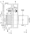
蒸着装置10は、第1の処理容器100および第2の処理容器200から構成されている。第1の処理容器100は、直方体の形状を有しており、第1〜第6の吹き出し機構110a〜110fを内蔵している。第1の処理容器100の内部では、この6つの吹き出し機構110から吹き出された気体分子により、基板Wに連続的に成膜処理が施される。
(Vapor deposition equipment)
The
各吹き出し機構110は、その長手方向が基板Wの幅と同等程度の長さを有し、形状および構造がすべて同一である。このように同一形状の6つの吹き出し機構110は、その長手方向が基板Wの進行方向に対して略垂直になるように互いに平行して等間隔に配置されている。
Each
各吹き出し機構110は、その上部に、気化された成膜材料を一時的に溜めておくバッファー空間Spを有し、その下部に、気化された成膜材料を輸送する輸送機構Trを有している。各吹き出し機構110の上面は、フレームFrにより塞がれている。フレームFrは、その周縁にてネジ止めされている。フレームFrの中央には、幅が1mmであるスリット状の開口が吹き出し口Opとして設けられていて、バッファー空間Spに溜まった成膜材料を吹き出し口Opから吹き出すようになっている。
Each
各吹き出し機構110の間には、隣り合う吹き出し機構110をそれぞれ仕切る7枚の隔壁120が設けられている。7枚の隔壁120は、同一形状を有した平板であって、隣り合う吹き出し機構110の対向する面Faから等距離の位置に等間隔に平行して配置されている。また、隣り合う吹き出し機構110の面Faに対向する各隔壁120の側面は、隣り合う吹き出し機構110の面Faより大きい。このようにして7つの隔壁120によって各吹き出し機構110を仕切ることにより、各吹き出し機構110の吹き出し口Opから吹き出される成膜材料の気体分子が、隣の吹き出し機構110の吹き出し口Opから吹き出される気体分子に混入することを防ぐようになっている。
Between each
基板Wは、第1の処理容器100内の天井部にて、図3に示したスライド機構130aに摺動可能に固定されたステージ130に静電吸着していて、第1の処理容器100の天井面に沿ってx軸方向に摺動するようになっている。
The substrate W is electrostatically attracted to the
第1の処理容器100には、図3に示したQCM(Quartz Crystal Microbalance)140が設けられている。以下に、QCMの簡単な原理について説明する。
The
水晶振動子表面に物質を付着させ、水晶振動体寸法、弾性率、密度等を等価的に変化させた場合、振動子の圧電気性質により以下の式で表される電気的共振周波数fの変化が起こる。
f=1/2t(√C/ρ) t:水晶片の厚み C:弾性定数 ρ:密度
When a substance is attached to the surface of the quartz vibrator and the quartz vibrator's size, elastic modulus, density, etc. are changed equivalently, the change in the electrical resonance frequency f expressed by the following equation depending on the piezoelectric properties of the vibrator Happens.
f = 1 / 2t (√C / ρ) t: thickness of crystal piece C: elastic constant ρ: density
この現象を利用し、水晶振動子の共振周波数の変化量により極めて微量な付着物を定量的に測定する。このように設計された水晶振動子の総称がQCMである。上式に示したように、周波数の変化は、付着物質による弾性定数の変化と物質の付着厚みを水晶密度に換算したときの厚み寸法で決まるものと考えられ、この結果、周波数の変化を付着物の重量に換算することができる。 By utilizing this phenomenon, an extremely small amount of adhered matter is quantitatively measured based on the amount of change in the resonance frequency of the crystal resonator. A general term for the crystal resonators thus designed is QCM. As shown in the above equation, the change in frequency is considered to be determined by the change in elastic constant due to the attached substance and the thickness dimension when the attached thickness of the substance is converted into the crystal density. It can be converted into the weight of the kimono.
第2の処理容器200は、略直方体の形状を有し、底部にて凹凸を有している。第2の処理容器200には、第1〜第6の容器210a〜210fが内蔵されていて、各容器210内には、3つの蒸着源がそれぞれ配設されている。たとえば、第6の容器210fには、蒸着源210f1、210f2、210f3が配設されている。各蒸着源は、形状および構造が同一であり、6つの連結管220a〜220fを介して第1〜第6の吹き出し機構110a〜110fとそれぞれ連結している。
The
各連結管220a〜220fには、第2の処理容器外(大気中)または第2の処理容器内(真空中)にて図示しないバルブがそれぞれ取り付けられていて、各バルブの開閉を操作することにより、各成膜材料(気体分子)を第1の処理容器100に供給するか否かを制御するようになっている。
Valves (not shown) are attached to the respective connecting
各蒸着源には、異なる種類の成膜材料が成膜の原料として納められていて、各蒸着源を、たとえば、200〜500℃程度の高温にすることにより、各種成膜材料を気化させるようになっている。 Each vapor deposition source stores different types of film forming materials as raw materials for film formation, and various vapor deposition materials are vaporized by setting each vapor deposition source to a high temperature of about 200 to 500 ° C., for example. It has become.
各蒸着源には、図示しないガス供給源から不活性ガス(たとえば、Arガス)が供給される。供給された不活性ガスは、各蒸着源にて気化された成膜材料の有機分子を、連結管220を介して吹き出し機構110まで運ぶキャリアガスとして機能する。
Each vapor deposition source is supplied with an inert gas (for example, Ar gas) from a gas supply source (not shown). The supplied inert gas functions as a carrier gas that carries organic molecules of the film forming material vaporized in each vapor deposition source to the
各蒸着源には、その底壁にヒータが埋め込まれているとともに、その側壁にヒータ(ともに図示せず)が埋め込まれていて、第1の処理容器100に内蔵されたQCM140から出力された信号に基づき、各成膜材料の気体分子の生成速度が求められ、求められた生成速度に基づき、底壁のヒータおよび側壁のヒータに印加する電圧が求められる。
Each deposition source has a heater embedded in its bottom wall and a heater (both not shown) embedded in its side wall, and a signal output from the
ここで、温度が高くなればなるほど、付着係数は小さくなるという減速に基づくと、温度が高くなればなるほど、連結管等に物理的に吸着する気体分子の数が少なくなる。この原理を利用して、底壁に埋め込まれたヒータの温度より側壁に埋め込まれたヒータの温度を高くする。このようにして、蒸着源210の成膜材料が納められた部分近傍の温度より、蒸着源210のその他の部分の温度を高くすることにより、成膜材料が気化して気体分子となって吹き出し機構110側に飛来する間に蒸着源210や連結管220に付着する気体分子の数を少なくすることができる。これにより、より多くの気体分子を吹き出し機構110から吹き出させ、基板Wに付着させることができる。
Here, based on the deceleration that the higher the temperature is, the smaller the adhesion coefficient is, the higher the temperature is, the smaller the number of gas molecules that are physically adsorbed on the connecting pipe or the like. Utilizing this principle, the temperature of the heater embedded in the side wall is made higher than the temperature of the heater embedded in the bottom wall. Thus, by raising the temperature of the other part of the
また、第1の処理容器100の内部および第2の処理容器200の内部は、図示しない排気装置により所定の真空度まで減圧されるようになっている。
Further, the inside of the
基板Wは、スライド機構130aにより各吹き出し機構110a〜110fのわずかに上方を、第1の吹き出し機構110aから第6の吹き出し機構110fに向けて所定の速度で移動する。これにより、基板Wには、第1〜第6の吹き出し機構110a〜110fからそれぞれ吹き出される異なる成膜材料によって、所望の異なる膜が6層積層されるようになっている。つぎに、この6層連続成膜処理時の蒸着装置10の具体的動作について説明する。
The substrate W is moved by the
(6層連続成膜処理)
図2は、蒸着装置10を用いて6層連続成膜処理を実行した結果、基板Wに積層される各層の状態を示している。まず、基板Wが、第1の吹き出し機構110aの上方をある速度で進行する際、第1の吹き出し機構110aから吹き出された成膜材料が基板Wに付着することにより、基板WのITO(Indium Tin Oxide:酸化インジウムスズ)からなる透明電極上に第1層のホール輸送層が形成される。
(6-layer continuous film forming process)
FIG. 2 shows a state of each layer stacked on the substrate W as a result of executing the six-layer continuous film forming process using the
このようにして、基板Wは、第1の吹き出し機構110a〜第6の吹き出し機構110fの上方を順に移動する。この結果、蒸着によりITO上にホール輸送層、非発光層、発光層および電子輸送層が形成される。これにより、同一容器内にて基板W上に6層の有機層が連続的に成膜される。
In this manner, the substrate W sequentially moves above the
(隔壁の形状および配置位置)
以上のようにして、1つの処理容器内に複数の蒸着源210を配設し、各蒸着源210により気化された成膜分子を基板Wに付着させることにより、基板W上に連続的に複数の異なる薄膜を形成する場合、隣り合う蒸着源210から気化された成膜分子が混ざり合い、各層の膜質が悪くなることが考えられる。
(Partition shape and location)
As described above, a plurality of
そこで、前述したように、各隔壁120は、隣り合う吹き出し機構の対向する面Faより大きい側面を有する。これにより、各吹き出し口Opから吹き出された成膜分子が各隔壁120を超えて隣の吹き出し口Op側へ飛来することを抑止する(すなわち、クロスコンタミネーションを抑止する)ことができる。
Therefore, as described above, each
また、このように吹き出し機構の対向する面より大きい側面を有する平板状の隔壁120の高さ、厚さ、隔壁上面と基板Wとの距離(ギャップ)および隔壁120の配置位置を最適化することにより、さらに、各隔壁120を超えて隣の吹き出し口Op側へ飛来する成膜分子(すなわち、コンタミネーション)の数を低減することができる。
In addition, the height and thickness of the
(隔壁の形状および配置位置を最適化するための実験1)
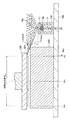
そこで、発明者は、隔壁120の形状および配置位置の最適化を図るために次のような実験を重ねた。まず、実験の処理条件について説明する。本実施形態にかかる蒸着装置10を簡略化した実験装置を図3に示す。このように、発明者は、蒸着装置10の第1の処理容器100の内部に吹き出し機構110および隔壁120を1つずつ内蔵し、第2の処理容器200の内部に蒸着源210を内蔵した実験装置を製作した。また、発明者は、吹き出し機構110と蒸着源210とを連結管220により連結した。蒸着源210には、成膜材料としてAlq3(aluminum−tris−8−hydroxyquinoline)の有機材料を0.1g収納した。
(
Therefore, the inventors repeated the following experiments in order to optimize the shape and arrangement position of the
また、発明者は、吹き出し機構110内部の吹き出し口Op付近に、キャリアガスとしてアルゴンガスを0.5sccm供給した。また、発明者らは、基板Wを静電吸着するために、ステージ130に4kVの高電圧HV(High Voltage)を印可した。また、基板Wの裏面の圧力BP(Back Pressure)を高めステージの熱を放熱するために、基板Wの裏面に40Torrのアルゴンガスを供給した。
Further, the inventor supplied 0.5 sccm of argon gas as a carrier gas in the vicinity of the blowout opening Op inside the
また、発明者らは、吹き出し機構110の中心軸から吹き出し機構110に対向する隔壁120の側面までのx軸方向の距離が60mmとなり、吹き出し口Opから隔壁120上面までの高さT(z軸方向の距離)が7mmとなるように隔壁120を配設した。その上で、発明者は、蒸着源210を200℃に昇温した後、ステージ130と隔壁120の上面とのギャップGを6mmにするようにステージ130を上下させるとともに、ステージ130のスライド機構130aをスライドさせて、吹き出し機構110の中心軸から基板Wの中心軸までのx軸方向の距離が121mmになるように基板Wを移動させた。
Further, the inventors set the distance in the x-axis direction from the central axis of the
その後、発明者は、蒸着源210の底部210aの温度を320℃、蒸着源210の上部210b、連結管220および吹き出し機構110の温度を340℃に設定し、各部の温度が設定温度に達したことを確認した。
Thereafter, the inventor set the temperature of the bottom 210a of the
蒸着源210に納められたAlq3は気化され、成膜分子となって連結管220から輸送機構Trを通り、吹き出し口Opから第1の処理容器100に放出された。このようにして放出されたAlq3の成膜分子は、吹き出し口Opの内外部の圧力差により直進しながら放射状に拡散し、基板Wの下面に付着した。
Alq 3 stored in the
その後、基板Wの下面の表面に付着した成膜材料(膜厚)を膜厚計により測定した。膜厚計の一例としては、光源から出力された光を被検体に形成された膜の上面と下面とに照射し、反射した2つ光の光路差により発生する干渉縞を捉え、これを解析して被検体の膜厚を検出する干渉計(たとえば、レーザ干渉計)やブロードの波長を照射して光のスペクトル情報から膜厚を算出する方法が挙げられる。その結果を図4のグラフJ1に示す。その後、発明者は、ステージ130のスライド機構130aをスライドさせて、吹き出し機構110の中心軸から基板Wの中心軸までのx軸方向の距離が111mmになるように基板Wを移動させ、同様の実験を行った。その結果を図4のグラフJ2に示す。
Thereafter, the film forming material (film thickness) adhering to the lower surface of the substrate W was measured with a film thickness meter. As an example of a film thickness meter, the light output from the light source is irradiated on the upper and lower surfaces of the film formed on the subject, and the interference fringes generated by the optical path difference between the two reflected lights are captured and analyzed. Then, an interferometer (for example, a laser interferometer) for detecting the film thickness of the subject or a method of calculating the film thickness from the spectral information of light by irradiating a broad wavelength. The result is shown in graph J1 in FIG. Thereafter, the inventor slides the
(実験1の結果)
実験の結果、図3の下方に基板Wの下面表面を示したように、吹き出し口Opから放射状に吹き出された成膜分子が最も遠くまで飛来したときに基板Wに付着するx軸方向の位置Maxより蒸着源側の面では、良質な膜が均一に形成された。また、図4に示したように、位置Maxから基板Wのほぼ中心までの面では、吹き出し機構110から離れれば離れるほど膜が薄くなることがわかった。一方、基板Wの中心付近より排気側の面では、膜厚はほぼ一様で、かつ、ほんのわずかに膜が形成された程度であった。
(Result of Experiment 1)
As a result of the experiment, as shown in the lower surface of the substrate W in the lower part of FIG. 3, the position in the x-axis direction that adheres to the substrate W when the film formation molecules blown radially from the blowing port Op fly farthest. A high-quality film was uniformly formed on the surface closer to the vapor deposition source than Max. In addition, as shown in FIG. 4, it has been found that on the surface from the position Max to almost the center of the substrate W, the film becomes thinner as the distance from the
この結果に基づき、発明者は、次のような考察を行った。図5に示したように、吹き出し口Opから吹き出されたAlq3の成膜分子は、放射状に拡散される。このとき、各成膜分子は、それぞれ直進する。吹き出し口Opから吹き出された成膜分子が拡散していく放射状のエリアのうち、一番外側を直線的に飛来した成膜分子Mmが基板に付着するためには、成膜分子Mmの最長飛距離が、成膜材料Alq3の平均自由工程よりも短い必要がある。ここで、基板Wと隔壁上部のギャップGが6mm、吹き出し口Opから各隔壁120上面までの高さTが7mm、吹き出し口Opから成膜分子Mmが付着したx方向の距離Mxが70mmであることから、成膜分子Mmの最長飛距離は、71.2(=(Mx2+(G+T)2)1/2)となる。
Based on this result, the inventor made the following consideration. As shown in FIG. 5, the Alq 3 film-forming molecules blown from the blow-out opening Op are diffused radially. At this time, each film-forming molecule goes straight. In the radial area where the film-forming molecules blown out from the blow-out opening Op diffuse, the film-forming molecules Mm that have come linearly from the outermost side adhere to the substrate. distance must be less than the mean free path of film forming material Alq 3. Here, the gap G between the substrate W and the upper part of the partition wall is 6 mm, the height T from the outlet Op to the upper surface of each
一方、平均自由工程MFPは、文献 真空技術講座12の真空技術常用諸表(日刊工業新聞社1965)にも記載されているように、以下の式で表される。
MFP=3.11×10⁻²⁴×T/P(δ)2×1000(mm)
ここで、Tは温度(K)、Pは圧力(Pa)、δは分子直径(m)である。
On the other hand, the mean free path MFP is expressed by the following equation as described in the vacuum technology regular tables (Nikkan Kogyo Shimbun 1965) of the literature vacuum technology course 12.
MFP = 3.11 × 10 −24 × T / P (δ) 2 × 1000 (mm)
Here, T is temperature (K), P is pressure (Pa), and δ is molecular diameter (m).
たとえば、上記文献(真空技術常用諸表)にも記載されているように、Arガスの分子直径は、3.67×10―10(m)であるから、Arガスの平均自由工程MFPは、温度Tが573.15(K)、圧力が0.01(Pa)のとき、1323.4(mm)となる。 For example, since the molecular diameter of Ar gas is 3.67 × 10 −10 (m) as described in the above-mentioned document (Vacuum Technology Common Use Tables), the mean free path MFP of Ar gas has a temperature of When T is 573.15 (K) and the pressure is 0.01 (Pa), it is 1323.4 (mm).
図6には、球状であるArガス、Alq3、α−NPDの成膜分子の平均自由工程が示されている。この表を見ると、気体分子の平均自由工程は、圧力に依存することがわかる。この表から、発明者は、蒸着装置10の内部圧力を0.01Pa以下にすれば、Arガス、Alq3、α−NPDの各平均自由工程は、1323.3(mm)、102.4(mm)、79(mm)以上となるので、最長飛行距離が71.2(mm)の成膜分子Mmは、飛来中に消滅することなく基板に付着することができる。この結果、基板Wの蒸着源側の端部Int(図5参照)から最長飛距離の成膜分子Mmが到達する位置Maxまでの面内にて、有機膜が均一に形成されることをつきとめた。なお、上述したように平均自由工程は圧力に依存するから、たとえば、圧力を0.01Paより小さくすれば、平均自由工程はより長くなる。このようにして、圧力を制御することにより、最長飛距離の成膜分子Mmを確実に基板まで到達させることができる。
FIG. 6 shows the mean free path of spherical Ar gas, Alq 3 , and α-NPD film forming molecules. From this table, it can be seen that the mean free path of gas molecules depends on the pressure. From this table, if the inventor sets the internal pressure of the
ここで、書籍名 薄膜光学(出版社 丸善株式会社 発行者 村田誠四郎 発行年月日 平成15年3月15日 発行 平成16年4月10日 第2刷発行)の記載によれば、基板上に入射した蒸発分子は、決してそのまま基板Wに付着して、降り積もるように膜を形成するわけではなく、入射した分子の一部は反射し、真空中に跳ね返される。また、表面に吸着した分子は表面上を動き回り、あるものは再び真空に飛び出し、あるものは基板Wのあるサイトにつかまって膜を形成する。 Here, according to the description of the book name Thin Film Optics (Publisher: Maruzen Co., Ltd. Publisher: Seishiro Murata, Issue Date: March 15, 2003 Issue: April 10, 2004, Second Print Issue) The evaporated molecules incident on the substrate never adhere to the substrate W as they are, and do not form a film so as to fall down. Some of the incident molecules are reflected and bounced back into the vacuum. Further, molecules adsorbed on the surface move around on the surface, and some of them are released into the vacuum again, and some of them are caught at a site on the substrate W to form a film.
よって、基板Wに付着した成膜分子のうち、あるものは再び飛び出し、基板Wと隔壁上部のギャップGの間を反射しながら進んでいき、基板Wと隔壁上面のいずれかの位置に再び付着する。このような分子の動きから、発明者は、最長飛距離の成膜分子Mmが到達する位置Maxから基板Wの中心付近Cntまでの面では、蒸着源側から離れるほど基板Wと隔壁上部のギャップGの間を反射しながら進んでいく分子の割合が、基板Wと隔壁上部のギャップGの間のいずれかに付着する分子Mの割合より少なくなるため、図3の下部および図4に示したように、膜厚が徐々に薄くなることを解明した。 Therefore, some of the deposition molecules attached to the substrate W jump out again, proceed while reflecting between the gap G between the substrate W and the upper part of the partition wall, and attach again to any position on the substrate W and the upper surface of the partition wall. To do. From such a movement of molecules, the inventor has found that the gap between the substrate W and the upper part of the partition wall becomes farther away from the deposition source side in the plane from the position Max where the film formation molecule Mm having the longest flight distance reaches to the center Cnt of the substrate W. Since the ratio of the molecules proceeding while reflecting between G is smaller than the ratio of the molecules M adhering to any of the gap W between the substrate W and the upper part of the partition wall, it is shown in the lower part of FIG. 3 and FIG. As shown, the film thickness was gradually reduced.
さらに、発明者は、基板Wの蒸着源側の端部Intから基板Wの中心付近Cntまでにほとんどすべての成膜分子が付着してしまい、基板Wの中心付近Cntから基板Wの排気側の端部Extでは、基板Wと隔壁上部のギャップGの間を反射しながら進んでいく分子Mがほとんどないため、図3の下部および図4に示したように、基板Wの中心付近Cntから基板Wの排気側の端部Extまでの面には、ほとんど成膜分子は付着しないことを解明した。 Furthermore, the inventor attaches almost all of the film forming molecules from the end portion Int on the evaporation source side of the substrate W to the vicinity of the center Cnt of the substrate W, and from the vicinity of the center of the substrate W to the exhaust side of the substrate W. At the end portion Ext, there is almost no molecule M that travels while reflecting between the gap W between the substrate W and the upper part of the partition wall, so that the substrate from the center Cnt of the substrate W to the substrate as shown in the lower part of FIG. It has been clarified that almost no film forming molecules adhere to the surface up to the end portion Ext on the exhaust side of W.
(実験2)
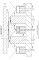
発明者は、成膜分子の直進性をさらに証明するために、図7に示したように、ギャップGを6mmから2mmにし、吹き出し機構110の中心から基板Wの中心までのx軸方向の距離が116mmになるようにステージ130の位置を変更させた状態にて再度実験を行った。
(Experiment 2)
In order to further prove the straightness of the film-forming molecules, the inventor changed the gap G from 6 mm to 2 mm as shown in FIG. 7, and the distance in the x-axis direction from the center of the
(実験2の結果)
実験後、発明者が、基板Wの全面にUV光を照射したところ、いずれからも光(hν)は発せられなかった。もし、Alq3の成膜分子が基板Wに付着していたら、照射したUV光のエネルギーにより、成膜分子Mが励起状態となり、その後、成膜分子Mが基底状態に戻るときに光(hν)が発せられることから、発明者は、ギャップGを6mmから2mmにし、吹き出し機構110の中心から基板Wの中心までのx軸方向の距離が116mmになるようにステージ130の位置を変更した場合、図7の下部に示したように、基板Wに材料は付着していなかったと結論付けた。
(Result of Experiment 2)
After the experiment, when the inventor irradiates the entire surface of the substrate W with UV light, no light (hν) was emitted from any of them. If Alq 3 film-forming molecules are attached to the substrate W, the energy of the irradiated UV light causes the film-forming molecules M to be in an excited state, and then light (hν) when the film-forming molecules M return to the ground state. ), The inventor changes the position of the
ギャップGを6mmから2mmに変更した場合、発明者は、基板Wに成膜分子が付着しなかった理由を、「成膜分子は直進する性質を有するためである」と考えた。具体的には、図8に示したように、発明者は、吹き出し口Opから吹き出された成膜分子のうち、直進しながら隔壁120に遮られずに最長距離を飛行した成膜分子Mmの到達位置Maxが、基板Wの吹き出し機構側の端部Intよりも吹き出し機構側であったこと、および、ギャップGが非常に小さいため、いずれかの位置に付着した成膜分子のうち、再び付着位置から離れ、基板Wと隔壁上面のギャップGの間を進入する成膜分子Mが非常に少ないこと、さらに、基板Wと隔壁上面のギャップGの間を進入する成膜分子の量が非常に少ないため、基板Wと隔壁上面とを反射しながらギャップ間を進んでいく分子Mはほとんど存在しないことが基板Wに成膜材料が付着しなかった理由であると結論付けた。
When the gap G was changed from 6 mm to 2 mm, the inventor considered that the reason why the film formation molecules did not adhere to the substrate W was “because the film formation molecules have a straight traveling property”. Specifically, as shown in FIG. 8, the inventor of the film formation molecules Mm blown out from the blowout opening Op and traveled the longest distance without being blocked by the
以上の実験から、発明者は、以下のように、隔壁120の形状および配置位置を最適化する関係を見いだした。すなわち、図9に示したように、吹き出し口Opから放出された成膜分子は、放射状にそれぞれ直進する。成膜分子が放射状に拡散されるエリアでは、基板Wに均一な膜が形成される。基板Wに付着した分子のうち、一部は、基板Wから離れて再び飛来し、基板Wと隔壁上面のギャップGの間を進入する。ギャップGの大きさによって、基板Wと隔壁上面のギャップGの間を進入する分子の量は異なる。ギャップGが2mmのとき、基板Wと隔壁上面のギャップGの間を進入する分子の量はほとんどなくなり、各吹き出し口Opから吹き出された成膜分子が、隣の吹き出し口Opから吹き出された成膜分子に混入し、膜質を劣化させるというクロスコンタミネーションの問題は生じない。したがって、基板Wと隔壁上部のギャップGは、2mm以下が好ましい。
From the above experiment, the inventor found a relationship for optimizing the shape and arrangement position of the
一方、ギャップが6mm以下であっても、隔壁120の形状および配置位置をつぎの2つ条件を満足するように最適化すれば、クロスコンタミネーションの問題は問題とならない程度となる。なお、つぎの2つの条件は、基板Wと隔壁上部のギャップGが2mm以下の場合であっても満たされる必要がある。
On the other hand, even if the gap is 6 mm or less, if the shape and arrangement position of the
1つ目は、成膜材料の最長飛距離は、成膜材料の平均自由工程よりも短いという条件である。これにより、各吹き出し口Opから吹き出され、放射状の拡散エリア内に拡散された成膜分子のうち、各隔壁120に遮られない成膜分子は、第1の処理容器100の空間中を飛来中に消滅することなく、すべて基板Wまで到達することができる。これにより、基板Wに良質な膜を均一に形成することができる。
The first condition is that the longest flight distance of the film forming material is shorter than the mean free path of the film forming material. Thereby, of the film forming molecules blown out from each blow-out opening Op and diffused in the radial diffusion area, film forming molecules not blocked by the
そして、2つ目は、各隔壁120に遮られずに直進しながら基板Wまで到達した最長飛距離の成膜材料Mmの到達位置(吹き出し機構110の中心位置から成膜材料Mmの到達位置までのx軸方向の距離X)は、隣り合う吹き出し機構110から等距離にある基板Wの位置(吹き出し機構110の中心位置から隣の隔壁120の中心位置までのx軸方向の距離E)よりも小さいという条件である。
The second is the arrival position of the film-forming material Mm with the longest flight distance that has reached the substrate W while moving straight without being blocked by each partition 120 (from the center position of the
これにより、各吹き出し口Opから吹き出された成膜分子のほとんどは、放射状の拡散エリア内に納められ、隣の吹き出し口Opから吹き出される成膜分子中に混入されない。これにより、各吹き出し口Opから吹き出された成膜分子のみから所望の特性の膜を基板W上に連続的に形成することができる。 Thereby, most of the film-forming molecules blown out from each blowing port Op are stored in the radial diffusion area, and are not mixed into the film-forming molecules blown out from the adjacent blowing port Op. As a result, a film having desired characteristics can be continuously formed on the substrate W only from the film-forming molecules blown from the respective blow-off ports Op.
この2つ目の条件を式にて表すと次のようになる。
E>X・・・(1)
This second condition is expressed as follows.
E> X (1)
ここで、隔壁120の厚みをDとすると、3角形の比例関係から、
(G+T)/T=X/(E−D/2)・・・(2)
となる。
Here, when the thickness of the
(G + T) / T = X / (ED / 2) (2)
It becomes.
式(2)を式(1)に代入すると、
X=(G+T)(E−D/2)/T<E・・・(3)
となる。
Substituting equation (2) into equation (1),
X = (G + T) (ED / 2) / T <E (3)
It becomes.
さらに、式(3)を変形すると、
E<(G+T)×D/2G・・・(4)
となる。
Furthermore, when equation (3) is transformed,
E <(G + T) × D / 2G (4)
It becomes.
このようにして求められた式(4)を満たすように、各隔壁120から基板WまでのギャップG、各吹き出し口Opから各隔壁120上面までの高さT、各隔壁120の厚みDおよび各蒸着源210(吹き出し機構110)の中心位置から各隔壁の中心位置までの距離Eを定めることにより、上述したクロスコンタミネーションを問題とならない程度まで減少させることができる。これにより、各層の特性を良好に保ちながら、同一処理容器内にて連続的に有機膜を形成することができる。
The gap G from each
この結果、同一処理容器内にて連続成膜するため、搬送中に基板Wに汚染物が付着することを低減することができる。この結果、クロスコンタミネーションを抑止しながら、基板W上に付着した汚染物の数を少なくすることによりエネルギー界面制御性を高くし、エネルギー障壁を低くすることができる。この結果、有機EL素子の発光強度(輝度)を向上させることができる。また、同一の処理容器内にて基板Wに連続成膜が施されることによりフットプリントを小さくすることができる。 As a result, since continuous film formation is performed in the same processing container, it is possible to reduce the adhesion of contaminants to the substrate W during transport. As a result, the energy interface controllability can be increased and the energy barrier can be lowered by reducing the number of contaminants adhering to the substrate W while suppressing cross contamination. As a result, the emission intensity (luminance) of the organic EL element can be improved. Moreover, a footprint can be made small by performing continuous film-forming on the board | substrate W within the same processing container.
なお、以上に説明した各実施形態における蒸着装置10にて成膜処理することが可能なガラス基板のサイズは、730mm×920mm以上である。たとえば、蒸着装置10は、730mm×920mm(チャンバ内の径:1000mm×1190mm)のG4.5基板サイズや、1100mm×1300mm(チャンバ内の径:1470mm×1590mm)のG5基板サイズを連続成膜処理することができる。また、蒸着装置10は、直径が、たとえば200mmや300mmのウエハを成膜処理することもできる。すなわち、成膜処理が施される被処理体には、ガラス基板やシリコンウエハが含まれる。
In addition, the size of the glass substrate which can be formed into a film by the
上記実施形態において、各部の動作はお互いに関連しており、互いの関連を考慮しながら、一連の動作として置き換えることができる。そして、このように置き換えることにより、蒸着装置の発明の実施形態を蒸着方法の実施形態とすることができる。 In the above embodiment, the operations of the respective units are related to each other, and can be replaced as a series of operations in consideration of the relationship between each other. And by substituting in this way, embodiment of invention of a vapor deposition apparatus can be made into embodiment of a vapor deposition method.
以上、添付図面を参照しながら本発明の好適な実施形態について説明したが、本発明は係る例に限定されないことは言うまでもない。当業者であれば、特許請求の範囲に記載された範疇内において、各種の変更例または修正例に想到し得ることは明らかであり、それらについても当然に本発明の技術的範囲に属するものと了解される。 As mentioned above, although preferred embodiment of this invention was described referring an accompanying drawing, it cannot be overemphasized that this invention is not limited to the example which concerns. It will be apparent to those skilled in the art that various changes and modifications can be made within the scope of the claims, and these are naturally within the technical scope of the present invention. Understood.
たとえば、上記実施形態にかかる蒸着装置10では、成膜材料にパウダー状(固体)の有機EL材料を用いて、基板W上に有機EL多層成膜処理を施した。しかし、本発明にかかる蒸着装置は、たとえば、成膜材料に主に液体の有機金属を用い、気化させた成膜材料を500〜700℃に加熱された被処理体上で分解させることにより、被処理体上に薄膜を成長させるMOCVD(Metal Organic Chemical Vapor Deposition:有機金属気相成長法)に用いることもできる。このように、本発明にかかる蒸着装置は、有機EL成膜材料または有機金属成膜材料を原料として蒸着により被処理体に有機EL膜または有機金属膜を形成する装置として用いてもよい。
For example, in the
また、本発明にかかる蒸着装置は、必ずしも吹き出し機構110(吹き出し口Op)と蒸着源210とが連結管220にて連結されている構造を有していなくてもよく、たとえば、吹き出し機構110が存在せず、蒸着源210に設けられた吹き出し口から成膜分子を放出する構造であってもよい。また、本発明にかかる蒸着装置は、必ずしも第1の処理容器100と第2の処理容器200とが別体となっている必要はなく、1つの処理容器内にて連続成膜するように構成されていてもよい。
In addition, the vapor deposition apparatus according to the present invention does not necessarily have a structure in which the blowing mechanism 110 (blowing port Op) and the
10 蒸着装置
100 第1の処理容器
110、110a〜110f 吹き出し機構
120 隔壁
130 ステージ
140 QCM
200 第2の処理容器
210、210a〜210f 蒸着源
220、220a〜220f 連結管
Op 吹き出し口
DESCRIPTION OF
200
Claims (8)
成膜材料を収納し、収納された成膜材料をそれぞれ気化させる複数の蒸着源と、
前記複数の蒸着源にそれぞれ連結され、吹き出し口を有し、前記複数の蒸着源にて気化された成膜材料を前記吹き出し口からそれぞれ吹き出す複数の吹き出し機構と、
前記複数の吹き出し機構のうち、隣り合う吹き出し機構の間に配置され、前記隣り合う吹き出し機構をそれぞれ仕切る1または2以上の隔壁とを備え、
前記1または2以上の隔壁は、
前記隣り合う吹き出し機構に設けられた吹き出し口から放射状に拡散される成膜材料のうち、各隔壁に遮られずに直進しながら被処理体まで到達した最長飛距離の成膜材料の到達位置が、前記隣り合う吹き出し機構から等距離にある被処理体上の位置よりも前記最長飛距離の成膜材料が吹き出された吹き出し口側に位置し、かつ、前記成膜材料の最長飛距離は、前記成膜材料の平均自由工程よりも短いという2つの条件を満たすように配置される蒸着装置。 A vapor deposition apparatus for film-forming a workpiece in a processing container by vapor deposition,
A plurality of vapor deposition sources for storing film forming materials and vaporizing each of the stored film forming materials;
A plurality of blowing mechanisms each connected to the plurality of vapor deposition sources, each having a blowout port, and blowing out the film-forming material vaporized in the plurality of vapor deposition sources from the blowout port;
Among the plurality of blowing mechanisms, provided between adjacent blowing mechanisms, comprising one or two or more partitions that partition the adjacent blowing mechanisms, respectively .
The one or more partition walls are
Among the film-forming materials that are diffused radially from the blow-off ports provided in the adjacent blow-off mechanisms, the arrival position of the film-forming material with the longest flight distance that has reached the object to be processed while traveling straight without being blocked by each partition wall is , Located on the outlet side from which the film-forming material of the longest flight distance is blown out from the position on the target object that is equidistant from the adjacent blow-off mechanism, and the longest flight distance of the film-forming material is: A vapor deposition apparatus arranged so as to satisfy two conditions of being shorter than the mean free path of the film forming material .
同一形状を有し、等間隔に平行して配置され、
前記1または2以上の隔壁は、
同一形状を有し、前記隣り合う吹き出し機構の間にて前記隣り合う吹き出し機構から等距離の位置に等間隔に平行して配置される請求項1に記載された蒸着装置。 The plurality of blowing mechanisms are
Have the same shape, arranged in parallel at equal intervals,
The one or more partition walls are
The vapor deposition apparatus of Claim 1 which has the same shape and is arrange | positioned in parallel at equal intervals in the position of equidistant from the said adjacent blowing mechanism between the said adjacent blowing mechanisms.
前記各隔壁の面が前記隣接する吹き出し機構の面より大きい請求項2に記載された蒸着装置。 The mutually facing surfaces of each partition and the blowing mechanism adjacent to each partition are:
The vapor deposition apparatus according to claim 2, wherein a surface of each partition wall is larger than a surface of the adjacent blowing mechanism.
前記各隔壁から被処理体までのギャップG、各吹き出し口から各隔壁上面までの高さT、前記各隔壁の厚みDおよび各蒸着源の中心位置から前記各隔壁の中心位置までの距離Eの関係が、E<(G+T)×D/2Gとなるように配置される請求項1に記載された蒸着装置。 Each of the partition walls is
The gap G from each partition to the object to be processed, the height T from each outlet to the top surface of each partition, the thickness D of each partition, and the distance E from the center position of each deposition source to the center position of each partition relationship, E <(G + T) × been deposited device according to claim 1 which is arranged so as to be D / 2G.
有機EL成膜材料または有機金属成膜材料を有機材料として被処理体に有機EL膜または有機金属膜のいずれかを形成する請求項1に記載された蒸着装置。 The vapor deposition apparatus comprises:
The vapor deposition apparatus according to claim 1 , wherein an organic EL film or an organic metal film is used as an organic material to form either an organic EL film or an organic metal film on a target object .
複数の蒸着源に収納された成膜材料をそれぞれ気化させ、
前記複数の蒸着源にそれぞれ連結された複数の吹き出し機構の吹き出し口から、前記複数の蒸着源にて気化された成膜材料をそれぞれ吹き出させ、
前記複数の吹き出し機構のうち、隣り合う吹き出し機構の間に設けられ、前記隣り合う吹き出し機構をそれぞれ仕切る1または2以上の隔壁であって、前記隣り合う吹き出し機構に設けられた吹き出し口から放射状に拡散される成膜材料のうち、各隔壁に遮られずに直進しながら被処理体まで到達した最長飛距離の成膜材料の到達位置が、前記隣り合う吹き出し機構から等距離にある被処理体上の位置よりも前記最長飛距離の成膜材料が吹き出された吹き出し口側に位置し、かつ、前記成膜材料の最長飛距離は、前記成膜材料の平均自由工程よりも短いという2つの条件を満たすように配置された前記1または2以上の隔壁により、各吹き出し口から吹き出された成膜材料が各隔壁を超えて隣の吹き出し口側へ飛来することを抑止しながら、気化された成膜材料により被処理体に膜を連続的に形成する蒸着方法。 A vapor deposition method for film-forming a workpiece in a processing container by vapor deposition,
Each of the film deposition materials stored in multiple evaporation sources is vaporized,
From the outlets of a plurality of blowing mechanisms respectively connected to the plurality of vapor deposition sources, the film-forming materials vaporized in the plurality of vapor deposition sources are blown out,
Among the plurality of blowing mechanisms, one or two or more partitions provided between adjacent blowing mechanisms and partitioning the neighboring blowing mechanisms, respectively, radially from the blowing ports provided in the neighboring blowing mechanisms Of the film forming material to be diffused, the object to be processed in which the reaching position of the film forming material having the longest flight distance that has reached the object to be processed while traveling straight without being blocked by each partition is equidistant from the adjacent blowing mechanism The longest flight distance of the film-forming material is shorter than the average free path of the film-forming material. by the one or more partition walls are arranged so as to satisfy the condition, while suppressing the film forming material blown out from the blowout opening is flying to the balloon mouth side of the next beyond the partition walls, Evaporation method for continuously forming a film on the target object by reduction depositions material.
Priority Applications (7)
| Application Number | Priority Date | Filing Date | Title |
|---|---|---|---|
| JP2007023402A JP5020650B2 (en) | 2007-02-01 | 2007-02-01 | Vapor deposition apparatus, vapor deposition method, and vapor deposition apparatus manufacturing method |
| PCT/JP2008/051395 WO2008093726A1 (en) | 2007-02-01 | 2008-01-30 | Deposition apparatus, deposition method and deposition apparatus manufacturing method |
| CN2008800037795A CN101600815B (en) | 2007-02-01 | 2008-01-30 | Deposition apparatus, deposition method and deposition apparatus manufacturing method |
| KR1020097018192A KR101212276B1 (en) | 2007-02-01 | 2008-01-30 | Deposition apparatus, deposition method and deposition apparatus manufacturing method |
| DE112008000313T DE112008000313T5 (en) | 2007-02-01 | 2008-01-30 | Bedampfungseinrichtung, vapor deposition and manufacturing process for the vapor deposition |
| US12/525,093 US20100104751A1 (en) | 2007-02-01 | 2008-01-30 | Evaporating apparatus, evaporating method and manufacturing method of evaporating apparatus |
| TW097103753A TW200907081A (en) | 2007-02-01 | 2008-01-31 | Vapor deposition system, vapor deposition method and manufacturing method of vapor deposition system |
Applications Claiming Priority (1)
| Application Number | Priority Date | Filing Date | Title |
|---|---|---|---|
| JP2007023402A JP5020650B2 (en) | 2007-02-01 | 2007-02-01 | Vapor deposition apparatus, vapor deposition method, and vapor deposition apparatus manufacturing method |
Publications (3)
| Publication Number | Publication Date |
|---|---|
| JP2008189951A JP2008189951A (en) | 2008-08-21 |
| JP2008189951A5 JP2008189951A5 (en) | 2009-05-28 |
| JP5020650B2 true JP5020650B2 (en) | 2012-09-05 |
Family
ID=39674034
Family Applications (1)
| Application Number | Title | Priority Date | Filing Date |
|---|---|---|---|
| JP2007023402A Expired - Fee Related JP5020650B2 (en) | 2007-02-01 | 2007-02-01 | Vapor deposition apparatus, vapor deposition method, and vapor deposition apparatus manufacturing method |
Country Status (7)
| Country | Link |
|---|---|
| US (1) | US20100104751A1 (en) |
| JP (1) | JP5020650B2 (en) |
| KR (1) | KR101212276B1 (en) |
| CN (1) | CN101600815B (en) |
| DE (1) | DE112008000313T5 (en) |
| TW (1) | TW200907081A (en) |
| WO (1) | WO2008093726A1 (en) |
Families Citing this family (11)
| Publication number | Priority date | Publication date | Assignee | Title |
|---|---|---|---|---|
| JP5179739B2 (en) * | 2006-09-27 | 2013-04-10 | 東京エレクトロン株式会社 | Vapor deposition apparatus, vapor deposition apparatus control apparatus, vapor deposition apparatus control method, and vapor deposition apparatus usage method |
| CN102171377A (en) * | 2008-09-30 | 2011-08-31 | 东京毅力科创株式会社 | Deposition apparatus, deposition method, and storage medium having program stored therein |
| JP2012169225A (en) * | 2011-02-16 | 2012-09-06 | Tokyo Electron Ltd | Deposition apparatus |
| JP2014095131A (en) * | 2012-11-09 | 2014-05-22 | Tokyo Electron Ltd | Film deposition apparatus |
| WO2015136857A1 (en) * | 2014-03-11 | 2015-09-17 | 株式会社Joled | Deposition apparatus, method for controlling same, deposition method using deposition apparatus, and device manufacturing method |
| CN108026630B (en) * | 2015-09-24 | 2020-07-07 | 夏普株式会社 | Vapor deposition source, vapor deposition device, and vapor deposition film production method |
| CN107604337A (en) * | 2017-08-28 | 2018-01-19 | 武汉华星光电半导体显示技术有限公司 | A kind of linear evaporation source arrangement for detecting and its method for detecting |
| CN107858651B (en) * | 2017-11-27 | 2020-02-04 | 合肥鑫晟光电科技有限公司 | Evaporation plating equipment |
| KR102229219B1 (en) * | 2019-10-29 | 2021-03-17 | 주식회사 파인에바 | Heating assembly for deposition apparatus |
| JP7473892B2 (en) * | 2020-03-10 | 2024-04-24 | 株式会社昭和真空 | Evaporation source |
| KR20230053660A (en) * | 2020-08-21 | 2023-04-21 | 어플라이드 머티어리얼스, 인코포레이티드 | A processing system for processing a flexible substrate and a method for measuring at least one of a property of the flexible substrate and a property of one or more coatings on the flexible substrate. |
Family Cites Families (10)
| Publication number | Priority date | Publication date | Assignee | Title |
|---|---|---|---|---|
| JPS5939665B2 (en) * | 1981-10-06 | 1984-09-25 | 工業技術院長 | Method of forming a solar heat absorption film on the surface of metal foil |
| JPS62230966A (en) * | 1986-04-01 | 1987-10-09 | Canon Inc | Device for growing crystal |
| JPS63230966A (en) | 1987-03-19 | 1988-09-27 | Nkk Corp | Photochemical prime mover device |
| JP3360098B2 (en) * | 1995-04-20 | 2002-12-24 | 東京エレクトロン株式会社 | Shower head structure of processing equipment |
| US6337102B1 (en) * | 1997-11-17 | 2002-01-08 | The Trustees Of Princeton University | Low pressure vapor phase deposition of organic thin films |
| JP3734239B2 (en) | 1999-04-02 | 2006-01-11 | キヤノン株式会社 | Organic film vacuum deposition mask regeneration method and apparatus |
| JP2003077662A (en) * | 2001-06-22 | 2003-03-14 | Junji Kido | Method and device for manufacturing organic electroluminescent element |
| JP4513329B2 (en) * | 2004-01-16 | 2010-07-28 | 東京エレクトロン株式会社 | Processing equipment |
| JP4911555B2 (en) * | 2005-04-07 | 2012-04-04 | 国立大学法人東北大学 | Film forming apparatus and film forming method |
| JP5173175B2 (en) * | 2006-09-29 | 2013-03-27 | 東京エレクトロン株式会社 | Vapor deposition equipment |
-
2007
- 2007-02-01 JP JP2007023402A patent/JP5020650B2/en not_active Expired - Fee Related
-
2008
- 2008-01-30 US US12/525,093 patent/US20100104751A1/en not_active Abandoned
- 2008-01-30 CN CN2008800037795A patent/CN101600815B/en not_active Expired - Fee Related
- 2008-01-30 DE DE112008000313T patent/DE112008000313T5/en not_active Ceased
- 2008-01-30 KR KR1020097018192A patent/KR101212276B1/en not_active IP Right Cessation
- 2008-01-30 WO PCT/JP2008/051395 patent/WO2008093726A1/en active Application Filing
- 2008-01-31 TW TW097103753A patent/TW200907081A/en unknown
Also Published As
| Publication number | Publication date |
|---|---|
| KR101212276B1 (en) | 2012-12-14 |
| TW200907081A (en) | 2009-02-16 |
| US20100104751A1 (en) | 2010-04-29 |
| JP2008189951A (en) | 2008-08-21 |
| WO2008093726A1 (en) | 2008-08-07 |
| CN101600815B (en) | 2012-03-28 |
| DE112008000313T5 (en) | 2009-12-17 |
| KR20090106649A (en) | 2009-10-09 |
| CN101600815A (en) | 2009-12-09 |
Similar Documents
| Publication | Publication Date | Title |
|---|---|---|
| JP5020650B2 (en) | Vapor deposition apparatus, vapor deposition method, and vapor deposition apparatus manufacturing method | |
| KR101075131B1 (en) | Evaporating apparatus, apparatus for controlling evaporating apparatus, method for controlling evaporating apparatus, method for using evaporating apparatus and method for manufacturing blowing port | |
| JP5179739B2 (en) | Vapor deposition apparatus, vapor deposition apparatus control apparatus, vapor deposition apparatus control method, and vapor deposition apparatus usage method | |
| KR100696547B1 (en) | Method for depositing film | |
| TWI421367B (en) | Film-forming apparatus, evaporation tool, and measuring method | |
| JP5452178B2 (en) | Vacuum deposition apparatus, vacuum deposition method, and organic EL display device manufacturing method | |
| TWI405860B (en) | Film-forming apparatus, film-forming system, film-forming method, and method of producing an electronic apparatus or an organic electroluminescence element | |
| JP5190446B2 (en) | Vapor deposition apparatus and control method of vapor deposition apparatus | |
| TWI415963B (en) | Film forming material and method of estimating a film forming material | |
| JPWO2006049022A1 (en) | Ion beam sputtering apparatus and method for forming multilayer film of reflective mask blank for EUV lithography | |
| JPWO2008120610A1 (en) | Vapor deposition source unit, vapor deposition apparatus, and temperature control apparatus for vapor deposition source unit | |
| JP5527933B2 (en) | Film forming apparatus control method, film forming method, film forming apparatus, organic EL electronic device, and storage medium storing control program thereof | |
| JP5095990B2 (en) | Substrate processing apparatus and cleaning method | |
| JP5875851B2 (en) | Thin film manufacturing method, thin film manufacturing apparatus | |
| US20090202708A1 (en) | Apparatus for Manufacturing Light Emitting Elements and Method of Manufacturing Light Emitting Elements | |
| JP5836974B2 (en) | Display device manufacturing apparatus and display device manufacturing method | |
| JP5412338B2 (en) | Mask cleaning apparatus, cleaning method, and organic EL manufacturing apparatus | |
| JP2008226472A (en) | Electronic device, its manufacturing method, structural body of sealing film, manufacturing device for manufacturing electronic device, and plasma processing device | |
| JP2008071938A (en) | Film-forming device | |
| JP2010163637A (en) | Film deposition apparatus and film deposition method | |
| JP5934604B2 (en) | Film forming apparatus and organic EL element manufacturing method | |
| WO2019037874A1 (en) | Apparatus for evaporating material in a vacuum chamber and method for evaporating material in a vacuum chamber | |
| JP2012193413A (en) | Vacuum deposition apparatus and method for forming thin film |
Legal Events
| Date | Code | Title | Description |
|---|---|---|---|
| A521 | Request for written amendment filed |
Free format text: JAPANESE INTERMEDIATE CODE: A523 Effective date: 20090415 |
|
| A621 | Written request for application examination |
Free format text: JAPANESE INTERMEDIATE CODE: A621 Effective date: 20090415 |
|
| A521 | Request for written amendment filed |
Free format text: JAPANESE INTERMEDIATE CODE: A523 Effective date: 20110701 |
|
| TRDD | Decision of grant or rejection written | ||
| A01 | Written decision to grant a patent or to grant a registration (utility model) |
Free format text: JAPANESE INTERMEDIATE CODE: A01 Effective date: 20120612 |
|
| A01 | Written decision to grant a patent or to grant a registration (utility model) |
Free format text: JAPANESE INTERMEDIATE CODE: A01 |
|
| A61 | First payment of annual fees (during grant procedure) |
Free format text: JAPANESE INTERMEDIATE CODE: A61 Effective date: 20120613 |
|
| R150 | Certificate of patent or registration of utility model |
Free format text: JAPANESE INTERMEDIATE CODE: R150 |
|
| FPAY | Renewal fee payment (event date is renewal date of database) |
Free format text: PAYMENT UNTIL: 20150622 Year of fee payment: 3 |
|
| R250 | Receipt of annual fees |
Free format text: JAPANESE INTERMEDIATE CODE: R250 |
|
| LAPS | Cancellation because of no payment of annual fees |