JP4977561B2 - 表示装置 - Google Patents
表示装置 Download PDFInfo
- Publication number
- JP4977561B2 JP4977561B2 JP2007229895A JP2007229895A JP4977561B2 JP 4977561 B2 JP4977561 B2 JP 4977561B2 JP 2007229895 A JP2007229895 A JP 2007229895A JP 2007229895 A JP2007229895 A JP 2007229895A JP 4977561 B2 JP4977561 B2 JP 4977561B2
- Authority
- JP
- Japan
- Prior art keywords
- organic
- layer
- lower electrode
- film
- ito
- Prior art date
- Legal status (The legal status is an assumption and is not a legal conclusion. Google has not performed a legal analysis and makes no representation as to the accuracy of the status listed.)
- Active
Links
- 239000011159 matrix material Substances 0.000 claims description 5
- 238000009751 slip forming Methods 0.000 claims description 3
- 239000010410 layer Substances 0.000 description 161
- 239000010408 film Substances 0.000 description 140
- 230000005525 hole transport Effects 0.000 description 19
- 238000004544 sputter deposition Methods 0.000 description 16
- 239000000758 substrate Substances 0.000 description 16
- 229910052751 metal Inorganic materials 0.000 description 11
- 239000002184 metal Substances 0.000 description 11
- 238000002161 passivation Methods 0.000 description 11
- 229910018507 Al—Ni Inorganic materials 0.000 description 10
- 229910045601 alloy Inorganic materials 0.000 description 10
- 239000000956 alloy Substances 0.000 description 10
- 238000005530 etching Methods 0.000 description 9
- 238000002347 injection Methods 0.000 description 9
- 239000007924 injection Substances 0.000 description 9
- XLOMVQKBTHCTTD-UHFFFAOYSA-N Zinc monoxide Chemical compound [Zn]=O XLOMVQKBTHCTTD-UHFFFAOYSA-N 0.000 description 7
- 229910052782 aluminium Inorganic materials 0.000 description 7
- 239000011521 glass Substances 0.000 description 7
- 238000000034 method Methods 0.000 description 7
- 239000010409 thin film Substances 0.000 description 7
- 238000007740 vapor deposition Methods 0.000 description 7
- 239000011701 zinc Substances 0.000 description 7
- QTBSBXVTEAMEQO-UHFFFAOYSA-N Acetic acid Chemical compound CC(O)=O QTBSBXVTEAMEQO-UHFFFAOYSA-N 0.000 description 6
- 239000011248 coating agent Substances 0.000 description 6
- 238000000576 coating method Methods 0.000 description 6
- 239000003086 colorant Substances 0.000 description 6
- 238000004519 manufacturing process Methods 0.000 description 6
- 229910000838 Al alloy Inorganic materials 0.000 description 5
- 229910018125 Al-Si Inorganic materials 0.000 description 5
- 229910021364 Al-Si alloy Inorganic materials 0.000 description 5
- 229910018520 Al—Si Inorganic materials 0.000 description 5
- 239000007983 Tris buffer Substances 0.000 description 5
- 239000002585 base Substances 0.000 description 5
- 239000011229 interlayer Substances 0.000 description 5
- 238000000206 photolithography Methods 0.000 description 5
- 239000004065 semiconductor Substances 0.000 description 5
- 229910018137 Al-Zn Inorganic materials 0.000 description 4
- 229910018573 Al—Zn Inorganic materials 0.000 description 4
- NBIIXXVUZAFLBC-UHFFFAOYSA-N Phosphoric acid Chemical compound OP(O)(O)=O NBIIXXVUZAFLBC-UHFFFAOYSA-N 0.000 description 4
- XAGFODPZIPBFFR-UHFFFAOYSA-N aluminium Chemical compound [Al] XAGFODPZIPBFFR-UHFFFAOYSA-N 0.000 description 4
- QVGXLLKOCUKJST-UHFFFAOYSA-N atomic oxygen Chemical compound [O] QVGXLLKOCUKJST-UHFFFAOYSA-N 0.000 description 4
- 230000015572 biosynthetic process Effects 0.000 description 4
- 238000010586 diagram Methods 0.000 description 4
- 238000009413 insulation Methods 0.000 description 4
- -1 lithium and cesium Chemical class 0.000 description 4
- 239000001301 oxygen Substances 0.000 description 4
- 229910052760 oxygen Inorganic materials 0.000 description 4
- 238000000059 patterning Methods 0.000 description 4
- 239000000126 substance Substances 0.000 description 4
- HCHKCACWOHOZIP-UHFFFAOYSA-N Zinc Chemical compound [Zn] HCHKCACWOHOZIP-UHFFFAOYSA-N 0.000 description 3
- 238000010549 co-Evaporation Methods 0.000 description 3
- 238000001312 dry etching Methods 0.000 description 3
- 230000000694 effects Effects 0.000 description 3
- 239000007789 gas Substances 0.000 description 3
- 239000000463 material Substances 0.000 description 3
- 229920002120 photoresistant polymer Polymers 0.000 description 3
- 229910052725 zinc Inorganic materials 0.000 description 3
- 239000011787 zinc oxide Substances 0.000 description 3
- 239000004925 Acrylic resin Substances 0.000 description 2
- 229920000178 Acrylic resin Polymers 0.000 description 2
- 229910018182 Al—Cu Inorganic materials 0.000 description 2
- OYPRJOBELJOOCE-UHFFFAOYSA-N Calcium Chemical compound [Ca] OYPRJOBELJOOCE-UHFFFAOYSA-N 0.000 description 2
- FYYHWMGAXLPEAU-UHFFFAOYSA-N Magnesium Chemical compound [Mg] FYYHWMGAXLPEAU-UHFFFAOYSA-N 0.000 description 2
- GRYLNZFGIOXLOG-UHFFFAOYSA-N Nitric acid Chemical compound O[N+]([O-])=O GRYLNZFGIOXLOG-UHFFFAOYSA-N 0.000 description 2
- 229910052783 alkali metal Inorganic materials 0.000 description 2
- 150000001340 alkali metals Chemical class 0.000 description 2
- 229910000147 aluminium phosphate Inorganic materials 0.000 description 2
- 150000001454 anthracenes Chemical class 0.000 description 2
- 229910052791 calcium Inorganic materials 0.000 description 2
- 239000011575 calcium Substances 0.000 description 2
- 125000000609 carbazolyl group Chemical class C1(=CC=CC=2C3=CC=CC=C3NC12)* 0.000 description 2
- 230000002950 deficient Effects 0.000 description 2
- 238000000151 deposition Methods 0.000 description 2
- 239000002019 doping agent Substances 0.000 description 2
- 238000000605 extraction Methods 0.000 description 2
- 229910052749 magnesium Inorganic materials 0.000 description 2
- 239000011777 magnesium Substances 0.000 description 2
- 230000000873 masking effect Effects 0.000 description 2
- VNWKTOKETHGBQD-UHFFFAOYSA-N methane Chemical compound C VNWKTOKETHGBQD-UHFFFAOYSA-N 0.000 description 2
- 229910017604 nitric acid Inorganic materials 0.000 description 2
- 230000003287 optical effect Effects 0.000 description 2
- TWNQGVIAIRXVLR-UHFFFAOYSA-N oxo(oxoalumanyloxy)alumane Chemical compound O=[Al]O[Al]=O TWNQGVIAIRXVLR-UHFFFAOYSA-N 0.000 description 2
- 238000007517 polishing process Methods 0.000 description 2
- 239000011347 resin Substances 0.000 description 2
- 229920005989 resin Polymers 0.000 description 2
- 229910052709 silver Inorganic materials 0.000 description 2
- 239000000243 solution Substances 0.000 description 2
- TVIVIEFSHFOWTE-UHFFFAOYSA-K tri(quinolin-8-yloxy)alumane Chemical compound [Al+3].C1=CN=C2C([O-])=CC=CC2=C1.C1=CN=C2C([O-])=CC=CC2=C1.C1=CN=C2C([O-])=CC=CC2=C1 TVIVIEFSHFOWTE-UHFFFAOYSA-K 0.000 description 2
- JIAARYAFYJHUJI-UHFFFAOYSA-L zinc dichloride Chemical compound [Cl-].[Cl-].[Zn+2] JIAARYAFYJHUJI-UHFFFAOYSA-L 0.000 description 2
- FQJQNLKWTRGIEB-UHFFFAOYSA-N 2-(4-tert-butylphenyl)-5-[3-[5-(4-tert-butylphenyl)-1,3,4-oxadiazol-2-yl]phenyl]-1,3,4-oxadiazole Chemical compound C1=CC(C(C)(C)C)=CC=C1C1=NN=C(C=2C=C(C=CC=2)C=2OC(=NN=2)C=2C=CC(=CC=2)C(C)(C)C)O1 FQJQNLKWTRGIEB-UHFFFAOYSA-N 0.000 description 1
- CFNMUZCFSDMZPQ-GHXNOFRVSA-N 7-[(z)-3-methyl-4-(4-methyl-5-oxo-2h-furan-2-yl)but-2-enoxy]chromen-2-one Chemical compound C=1C=C2C=CC(=O)OC2=CC=1OC/C=C(/C)CC1OC(=O)C(C)=C1 CFNMUZCFSDMZPQ-GHXNOFRVSA-N 0.000 description 1
- KZBUYRJDOAKODT-UHFFFAOYSA-N Chlorine Chemical compound ClCl KZBUYRJDOAKODT-UHFFFAOYSA-N 0.000 description 1
- GYHNNYVSQQEPJS-UHFFFAOYSA-N Gallium Chemical compound [Ga] GYHNNYVSQQEPJS-UHFFFAOYSA-N 0.000 description 1
- WHXSMMKQMYFTQS-UHFFFAOYSA-N Lithium Chemical compound [Li] WHXSMMKQMYFTQS-UHFFFAOYSA-N 0.000 description 1
- 229910000583 Nd alloy Inorganic materials 0.000 description 1
- 229910052779 Neodymium Inorganic materials 0.000 description 1
- 229910004298 SiO 2 Inorganic materials 0.000 description 1
- PTFCDOFLOPIGGS-UHFFFAOYSA-N Zinc dication Chemical compound [Zn+2] PTFCDOFLOPIGGS-UHFFFAOYSA-N 0.000 description 1
- 239000002253 acid Substances 0.000 description 1
- NIXOWILDQLNWCW-UHFFFAOYSA-N acrylic acid group Chemical group C(C=C)(=O)O NIXOWILDQLNWCW-UHFFFAOYSA-N 0.000 description 1
- 230000002411 adverse Effects 0.000 description 1
- 229910052784 alkaline earth metal Inorganic materials 0.000 description 1
- 150000001342 alkaline earth metals Chemical class 0.000 description 1
- 125000003277 amino group Chemical group 0.000 description 1
- 229910021417 amorphous silicon Inorganic materials 0.000 description 1
- 125000005605 benzo group Chemical group 0.000 description 1
- 230000000903 blocking effect Effects 0.000 description 1
- XZCJVWCMJYNSQO-UHFFFAOYSA-N butyl pbd Chemical compound C1=CC(C(C)(C)C)=CC=C1C1=NN=C(C=2C=CC(=CC=2)C=2C=CC=CC=2)O1 XZCJVWCMJYNSQO-UHFFFAOYSA-N 0.000 description 1
- 229910052792 caesium Inorganic materials 0.000 description 1
- TVFDJXOCXUVLDH-UHFFFAOYSA-N caesium atom Chemical compound [Cs] TVFDJXOCXUVLDH-UHFFFAOYSA-N 0.000 description 1
- 150000004649 carbonic acid derivatives Chemical class 0.000 description 1
- 150000001875 compounds Chemical class 0.000 description 1
- 230000008021 deposition Effects 0.000 description 1
- 238000007599 discharging Methods 0.000 description 1
- 230000001747 exhibiting effect Effects 0.000 description 1
- 229910052733 gallium Inorganic materials 0.000 description 1
- 150000004820 halides Chemical class 0.000 description 1
- RBTKNAXYKSUFRK-UHFFFAOYSA-N heliogen blue Chemical class [Cu].[N-]1C2=C(C=CC=C3)C3=C1N=C([N-]1)C3=CC=CC=C3C1=NC([N-]1)=C(C=CC=C3)C3=C1N=C([N-]1)C3=CC=CC=C3C1=N2 RBTKNAXYKSUFRK-UHFFFAOYSA-N 0.000 description 1
- 150000007857 hydrazones Chemical class 0.000 description 1
- 150000002460 imidazoles Chemical class 0.000 description 1
- 239000012535 impurity Substances 0.000 description 1
- 229910052738 indium Inorganic materials 0.000 description 1
- APFVFJFRJDLVQX-UHFFFAOYSA-N indium atom Chemical compound [In] APFVFJFRJDLVQX-UHFFFAOYSA-N 0.000 description 1
- 229910052741 iridium Inorganic materials 0.000 description 1
- GKOZUEZYRPOHIO-UHFFFAOYSA-N iridium atom Chemical compound [Ir] GKOZUEZYRPOHIO-UHFFFAOYSA-N 0.000 description 1
- 238000005224 laser annealing Methods 0.000 description 1
- 229910052744 lithium Inorganic materials 0.000 description 1
- 239000012528 membrane Substances 0.000 description 1
- 229910044991 metal oxide Inorganic materials 0.000 description 1
- 150000004706 metal oxides Chemical class 0.000 description 1
- 150000002739 metals Chemical class 0.000 description 1
- DCZNSJVFOQPSRV-UHFFFAOYSA-N n,n-diphenyl-4-[4-(n-phenylanilino)phenyl]aniline Chemical compound C1=CC=CC=C1N(C=1C=CC(=CC=1)C=1C=CC(=CC=1)N(C=1C=CC=CC=1)C=1C=CC=CC=1)C1=CC=CC=C1 DCZNSJVFOQPSRV-UHFFFAOYSA-N 0.000 description 1
- 238000001579 optical reflectometry Methods 0.000 description 1
- 150000004866 oxadiazoles Chemical class 0.000 description 1
- SIOXPEMLGUPBBT-UHFFFAOYSA-N picolinic acid Chemical class OC(=O)C1=CC=CC=N1 SIOXPEMLGUPBBT-UHFFFAOYSA-N 0.000 description 1
- 238000001020 plasma etching Methods 0.000 description 1
- 229910021420 polycrystalline silicon Inorganic materials 0.000 description 1
- 229920000123 polythiophene Polymers 0.000 description 1
- 125000004309 pyranyl group Chemical class O1C(C=CC=C1)* 0.000 description 1
- 229910052761 rare earth metal Inorganic materials 0.000 description 1
- 150000002910 rare earth metals Chemical class 0.000 description 1
- 238000005215 recombination Methods 0.000 description 1
- 230000006798 recombination Effects 0.000 description 1
- 238000002310 reflectometry Methods 0.000 description 1
- 238000007789 sealing Methods 0.000 description 1
- 238000000926 separation method Methods 0.000 description 1
- 239000002356 single layer Substances 0.000 description 1
- 238000005507 spraying Methods 0.000 description 1
- JBQYATWDVHIOAR-UHFFFAOYSA-N tellanylidenegermanium Chemical compound [Te]=[Ge] JBQYATWDVHIOAR-UHFFFAOYSA-N 0.000 description 1
- 150000003852 triazoles Chemical class 0.000 description 1
- XLYOFNOQVPJJNP-UHFFFAOYSA-N water Substances O XLYOFNOQVPJJNP-UHFFFAOYSA-N 0.000 description 1
- 235000005074 zinc chloride Nutrition 0.000 description 1
- 239000011592 zinc chloride Substances 0.000 description 1
- QEPMORHSGFRDLW-UHFFFAOYSA-L zinc;2-(2-hydroxyphenyl)-3h-1,3-benzoxazole-2-carboxylate Chemical class [Zn+2].OC1=CC=CC=C1C1(C([O-])=O)OC2=CC=CC=C2N1.OC1=CC=CC=C1C1(C([O-])=O)OC2=CC=CC=C2N1 QEPMORHSGFRDLW-UHFFFAOYSA-L 0.000 description 1
Images


Classifications
-
- H—ELECTRICITY
- H10—SEMICONDUCTOR DEVICES; ELECTRIC SOLID-STATE DEVICES NOT OTHERWISE PROVIDED FOR
- H10K—ORGANIC ELECTRIC SOLID-STATE DEVICES
- H10K59/00—Integrated devices, or assemblies of multiple devices, comprising at least one organic light-emitting element covered by group H10K50/00
- H10K59/80—Constructional details
- H10K59/805—Electrodes
- H10K59/8051—Anodes
- H10K59/80518—Reflective anodes, e.g. ITO combined with thick metallic layers
-
- H—ELECTRICITY
- H10—SEMICONDUCTOR DEVICES; ELECTRIC SOLID-STATE DEVICES NOT OTHERWISE PROVIDED FOR
- H10K—ORGANIC ELECTRIC SOLID-STATE DEVICES
- H10K50/00—Organic light-emitting devices
- H10K50/80—Constructional details
- H10K50/805—Electrodes
- H10K50/81—Anodes
- H10K50/818—Reflective anodes, e.g. ITO combined with thick metallic layers
-
- H—ELECTRICITY
- H10—SEMICONDUCTOR DEVICES; ELECTRIC SOLID-STATE DEVICES NOT OTHERWISE PROVIDED FOR
- H10K—ORGANIC ELECTRIC SOLID-STATE DEVICES
- H10K2102/00—Constructional details relating to the organic devices covered by this subclass
- H10K2102/301—Details of OLEDs
- H10K2102/302—Details of OLEDs of OLED structures
- H10K2102/3023—Direction of light emission
- H10K2102/3026—Top emission
-
- H—ELECTRICITY
- H10—SEMICONDUCTOR DEVICES; ELECTRIC SOLID-STATE DEVICES NOT OTHERWISE PROVIDED FOR
- H10K—ORGANIC ELECTRIC SOLID-STATE DEVICES
- H10K50/00—Organic light-emitting devices
- H10K50/80—Constructional details
- H10K50/805—Electrodes
- H10K50/82—Cathodes
- H10K50/828—Transparent cathodes, e.g. comprising thin metal layers
-
- H—ELECTRICITY
- H10—SEMICONDUCTOR DEVICES; ELECTRIC SOLID-STATE DEVICES NOT OTHERWISE PROVIDED FOR
- H10K—ORGANIC ELECTRIC SOLID-STATE DEVICES
- H10K59/00—Integrated devices, or assemblies of multiple devices, comprising at least one organic light-emitting element covered by group H10K50/00
- H10K59/10—OLED displays
- H10K59/12—Active-matrix OLED [AMOLED] displays
- H10K59/122—Pixel-defining structures or layers, e.g. banks
-
- H—ELECTRICITY
- H10—SEMICONDUCTOR DEVICES; ELECTRIC SOLID-STATE DEVICES NOT OTHERWISE PROVIDED FOR
- H10K—ORGANIC ELECTRIC SOLID-STATE DEVICES
- H10K59/00—Integrated devices, or assemblies of multiple devices, comprising at least one organic light-emitting element covered by group H10K50/00
- H10K59/80—Constructional details
- H10K59/805—Electrodes
- H10K59/8052—Cathodes
- H10K59/80524—Transparent cathodes, e.g. comprising thin metal layers
Description
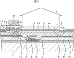
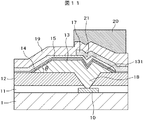
して所望の厚さに形成することが記載されている。「特許文献1」に記載の技術では、ITOを被着したあと、各画素毎にITOをフォトリソグラフィによってパターニングする必要があり、コストが嵩む。また、ITOをパターニングすることによるエッチング残渣等が生じやすい。さらに、ITOを最短発光波長λの1/4以下にまで研磨する必要があるが、この研磨工程のコスト、研磨工程による工程不良等も問題になる。
Claims (2)
- 下部電極、有機EL層、上部電極を有する画素がマトリクス状に形成されて表示部が構成され前記下部電極間を画素毎に絶縁膜で分離して構成された表示部と、前記表示部の外側に形成された端子とを備えた有機EL表示装置であって、
前記下部電極と前記有機EL層の間に透明導電膜を有し、
前記透明導電膜は、第1の前記下部電極と前記第1の下部電極に隣接する第2の前記下部電極との間であって、前記絶縁膜の上にも連続して形成されており、
前記透明導電膜は第1の前記端子と第2の前記端子の間にも連続膜として形成され、
前記透明導電膜は膜厚が5〜20nmであって、抵抗率が1〜10 5 Ω・cmであることを特徴とする有機EL表示装置。 - 前記透明導電膜は膜厚が10〜20nmであって、抵抗率が1〜10 5 Ω・cmであることを特徴とする請求項1に記載の有機EL表示装置。
Priority Applications (2)
| Application Number | Priority Date | Filing Date | Title |
|---|---|---|---|
| JP2007229895A JP4977561B2 (ja) | 2007-09-05 | 2007-09-05 | 表示装置 |
| US12/230,768 US20090058283A1 (en) | 2007-09-05 | 2008-09-04 | Display device |
Applications Claiming Priority (1)
| Application Number | Priority Date | Filing Date | Title |
|---|---|---|---|
| JP2007229895A JP4977561B2 (ja) | 2007-09-05 | 2007-09-05 | 表示装置 |
Publications (3)
| Publication Number | Publication Date |
|---|---|
| JP2009064612A JP2009064612A (ja) | 2009-03-26 |
| JP2009064612A5 JP2009064612A5 (ja) | 2010-10-21 |
| JP4977561B2 true JP4977561B2 (ja) | 2012-07-18 |
Family
ID=40406366
Family Applications (1)
| Application Number | Title | Priority Date | Filing Date |
|---|---|---|---|
| JP2007229895A Active JP4977561B2 (ja) | 2007-09-05 | 2007-09-05 | 表示装置 |
Country Status (2)
| Country | Link |
|---|---|
| US (1) | US20090058283A1 (ja) |
| JP (1) | JP4977561B2 (ja) |
Families Citing this family (16)
| Publication number | Priority date | Publication date | Assignee | Title |
|---|---|---|---|---|
| KR101570471B1 (ko) * | 2008-09-18 | 2015-11-23 | 삼성디스플레이 주식회사 | 유기발광 표시장치 및 이의 제조 방법 |
| JP2010080800A (ja) * | 2008-09-29 | 2010-04-08 | Seiko Instruments Inc | 発光デバイス及びその製造方法 |
| JP5401132B2 (ja) | 2009-01-20 | 2014-01-29 | 信越ポリマー株式会社 | 電波透過性装飾部材およびその製造方法 |
| JP5346632B2 (ja) * | 2009-03-17 | 2013-11-20 | 信越ポリマー株式会社 | 電波透過性加飾フィルムおよびこれを用いた装飾部材 |
| JP5503729B2 (ja) * | 2010-03-09 | 2014-05-28 | 太陽誘電株式会社 | 導体構造、透明デバイス及び電子機器 |
| KR101995700B1 (ko) * | 2011-06-24 | 2019-07-03 | 가부시키가이샤 한도오따이 에네루기 켄큐쇼 | 발광 패널, 발광 패널을 사용한 발광 장치 및 발광 패널의 제작 방법 |
| KR101871227B1 (ko) * | 2011-08-12 | 2018-08-03 | 삼성디스플레이 주식회사 | 유기 발광 소자 및 그 제조 방법 |
| KR101970540B1 (ko) * | 2012-11-15 | 2019-08-14 | 삼성디스플레이 주식회사 | 유기 발광 표시 장치 및 이의 제조 방법 |
| JP6155020B2 (ja) * | 2012-12-21 | 2017-06-28 | 株式会社半導体エネルギー研究所 | 発光装置及びその製造方法 |
| CN104157675A (zh) * | 2014-08-05 | 2014-11-19 | 京东方科技集团股份有限公司 | 一种oled显示器件及其制作方法、显示装置 |
| KR102151475B1 (ko) * | 2014-09-04 | 2020-09-04 | 엘지디스플레이 주식회사 | 유기발광표시패널 및 그 제조방법 |
| KR102060471B1 (ko) * | 2017-02-01 | 2019-12-30 | 엘지전자 주식회사 | 반도체 발광 소자를 이용한 디스플레이 장치 및 이의 제조 방법 |
| JP2018181970A (ja) * | 2017-04-07 | 2018-11-15 | 株式会社ジャパンディスプレイ | 表示装置、及び表示装置の製造方法 |
| CN108172600B (zh) * | 2017-12-29 | 2020-01-17 | 深圳市华星光电半导体显示技术有限公司 | 用于woled显示器的彩膜基板及woled显示器 |
| KR20200066959A (ko) * | 2018-12-03 | 2020-06-11 | 엘지디스플레이 주식회사 | 투명표시장치 |
| US11380864B2 (en) * | 2019-02-13 | 2022-07-05 | Canon Kabushiki Kaisha | Electronic device, display apparatus, photoelectric conversion apparatus, electronic apparatus, illumination apparatus, and moving object |
Family Cites Families (6)
| Publication number | Priority date | Publication date | Assignee | Title |
|---|---|---|---|---|
| US6956324B2 (en) * | 2000-08-04 | 2005-10-18 | Semiconductor Energy Laboratory Co., Ltd. | Semiconductor device and manufacturing method therefor |
| JP3708916B2 (ja) * | 2001-08-24 | 2005-10-19 | 株式会社半導体エネルギー研究所 | 発光装置 |
| JP4089544B2 (ja) * | 2002-12-11 | 2008-05-28 | ソニー株式会社 | 表示装置及び表示装置の製造方法 |
| JP2005197009A (ja) * | 2003-12-26 | 2005-07-21 | Sanyo Electric Co Ltd | 表示装置及びその製造方法及び製造装置 |
| JP4555727B2 (ja) * | 2005-04-22 | 2010-10-06 | 株式会社 日立ディスプレイズ | 有機発光表示装置 |
| JP5007170B2 (ja) * | 2007-07-20 | 2012-08-22 | 株式会社ジャパンディスプレイイースト | 有機el表示装置 |
-
2007
- 2007-09-05 JP JP2007229895A patent/JP4977561B2/ja active Active
-
2008
- 2008-09-04 US US12/230,768 patent/US20090058283A1/en not_active Abandoned
Also Published As
| Publication number | Publication date |
|---|---|
| JP2009064612A (ja) | 2009-03-26 |
| US20090058283A1 (en) | 2009-03-05 |
Similar Documents
| Publication | Publication Date | Title |
|---|---|---|
| JP4977561B2 (ja) | 表示装置 | |
| JP2009058897A (ja) | 表示装置 | |
| US10096662B2 (en) | Organic light emitting display device including a tandem structure and method of manufacturing the organic light emitting display device including the tandem structure | |
| US8212258B2 (en) | Display device and method for manufacturing display device | |
| US10734461B2 (en) | Thin film transistor array panel and organic light emitting diode display including the same | |
| US10727292B2 (en) | OLED with buffer layer over emitting layer | |
| KR100667081B1 (ko) | 유기전계발광표시장치 및 그의 제조방법 | |
| CN109980122B (zh) | 电致发光显示设备 | |
| JP2008124316A (ja) | 有機el表示装置 | |
| JP2005056846A (ja) | 有機電界発光素子及びその製造方法 | |
| JP4165145B2 (ja) | 有機発光表示装置 | |
| JP2008130363A (ja) | 有機el素子およびその製造方法、ならびに有機elディスプレイおよびその製造方法 | |
| JP2010062233A (ja) | 表示装置 | |
| JP5007170B2 (ja) | 有機el表示装置 | |
| KR20220129601A (ko) | 미러를 갖는 oled(organic light-emitting diode) 디스플레이 디바이스들 및 이를 제조하기 위한 방법 | |
| JP2011048973A (ja) | 有機el表示装置 | |
| JP2011034931A (ja) | 有機el表示装置 | |
| JP2006164737A (ja) | 表示素子、若しくはそれを備えた表示パネル及び表示装置 | |
| US20240122033A1 (en) | Display device and manufacturing method of the same | |
| US20240121994A1 (en) | Display device and manufacturing method of the same | |
| JP2019133835A (ja) | 有機el表示パネル及び有機el表示パネルの製造方法 | |
| JP5642841B2 (ja) | 有機el素子、若しくはそれを備えた表示パネル及び表示装置 | |
| US11588129B2 (en) | Organic light-emitting diode display device and manufacturing method thereof | |
| JP2008198491A (ja) | 有機elディスプレイパネルおよびその製造方法 | |
| JP5427253B2 (ja) | 有機el素子、若しくはそれを備えた表示パネル及び表示装置 |
Legal Events
| Date | Code | Title | Description |
|---|---|---|---|
| A521 | Request for written amendment filed |
Free format text: JAPANESE INTERMEDIATE CODE: A523 Effective date: 20100903 |
|
| A621 | Written request for application examination |
Free format text: JAPANESE INTERMEDIATE CODE: A621 Effective date: 20100903 |
|
| A711 | Notification of change in applicant |
Free format text: JAPANESE INTERMEDIATE CODE: A712 Effective date: 20110218 |
|
| RD03 | Notification of appointment of power of attorney |
Free format text: JAPANESE INTERMEDIATE CODE: A7423 Effective date: 20110218 |
|
| A977 | Report on retrieval |
Free format text: JAPANESE INTERMEDIATE CODE: A971007 Effective date: 20111227 |
|
| A131 | Notification of reasons for refusal |
Free format text: JAPANESE INTERMEDIATE CODE: A131 Effective date: 20120105 |
|
| A521 | Request for written amendment filed |
Free format text: JAPANESE INTERMEDIATE CODE: A523 Effective date: 20120227 |
|
| TRDD | Decision of grant or rejection written | ||
| A01 | Written decision to grant a patent or to grant a registration (utility model) |
Free format text: JAPANESE INTERMEDIATE CODE: A01 Effective date: 20120321 |
|
| A01 | Written decision to grant a patent or to grant a registration (utility model) |
Free format text: JAPANESE INTERMEDIATE CODE: A01 |
|
| A61 | First payment of annual fees (during grant procedure) |
Free format text: JAPANESE INTERMEDIATE CODE: A61 Effective date: 20120416 |
|
| R150 | Certificate of patent or registration of utility model |
Ref document number: 4977561 Country of ref document: JP Free format text: JAPANESE INTERMEDIATE CODE: R150 Free format text: JAPANESE INTERMEDIATE CODE: R150 |
|
| FPAY | Renewal fee payment (event date is renewal date of database) |
Free format text: PAYMENT UNTIL: 20150420 Year of fee payment: 3 |
|
| R250 | Receipt of annual fees |
Free format text: JAPANESE INTERMEDIATE CODE: R250 |
|
| R250 | Receipt of annual fees |
Free format text: JAPANESE INTERMEDIATE CODE: R250 |
|
| R250 | Receipt of annual fees |
Free format text: JAPANESE INTERMEDIATE CODE: R250 |
|
| R250 | Receipt of annual fees |
Free format text: JAPANESE INTERMEDIATE CODE: R250 |
|
| S531 | Written request for registration of change of domicile |
Free format text: JAPANESE INTERMEDIATE CODE: R313531 |
|
| S533 | Written request for registration of change of name |
Free format text: JAPANESE INTERMEDIATE CODE: R313533 |
|
| S111 | Request for change of ownership or part of ownership |
Free format text: JAPANESE INTERMEDIATE CODE: R313113 |
|
| R350 | Written notification of registration of transfer |
Free format text: JAPANESE INTERMEDIATE CODE: R350 |
|
| R350 | Written notification of registration of transfer |
Free format text: JAPANESE INTERMEDIATE CODE: R350 |
|
| R250 | Receipt of annual fees |
Free format text: JAPANESE INTERMEDIATE CODE: R250 |
|
| R250 | Receipt of annual fees |
Free format text: JAPANESE INTERMEDIATE CODE: R250 |
|
| R250 | Receipt of annual fees |
Free format text: JAPANESE INTERMEDIATE CODE: R250 |
|
| R250 | Receipt of annual fees |
Free format text: JAPANESE INTERMEDIATE CODE: R250 |
|
| R250 | Receipt of annual fees |
Free format text: JAPANESE INTERMEDIATE CODE: R250 |
|
| R250 | Receipt of annual fees |
Free format text: JAPANESE INTERMEDIATE CODE: R250 |