JP4977561B2 - Display device - Google Patents
Display device Download PDFInfo
- Publication number
- JP4977561B2 JP4977561B2 JP2007229895A JP2007229895A JP4977561B2 JP 4977561 B2 JP4977561 B2 JP 4977561B2 JP 2007229895 A JP2007229895 A JP 2007229895A JP 2007229895 A JP2007229895 A JP 2007229895A JP 4977561 B2 JP4977561 B2 JP 4977561B2
- Authority
- JP
- Japan
- Prior art keywords
- organic
- layer
- lower electrode
- film
- ito
- Prior art date
- Legal status (The legal status is an assumption and is not a legal conclusion. Google has not performed a legal analysis and makes no representation as to the accuracy of the status listed.)
- Active
Links
- 239000011159 matrix material Substances 0.000 claims description 5
- 238000009751 slip forming Methods 0.000 claims description 3
- 239000010410 layer Substances 0.000 description 161
- 239000010408 film Substances 0.000 description 140
- 230000005525 hole transport Effects 0.000 description 19
- 238000004544 sputter deposition Methods 0.000 description 16
- 239000000758 substrate Substances 0.000 description 16
- 229910052751 metal Inorganic materials 0.000 description 11
- 239000002184 metal Substances 0.000 description 11
- 238000002161 passivation Methods 0.000 description 11
- 229910018507 Al—Ni Inorganic materials 0.000 description 10
- 229910045601 alloy Inorganic materials 0.000 description 10
- 239000000956 alloy Substances 0.000 description 10
- 238000005530 etching Methods 0.000 description 9
- 238000002347 injection Methods 0.000 description 9
- 239000007924 injection Substances 0.000 description 9
- XLOMVQKBTHCTTD-UHFFFAOYSA-N Zinc monoxide Chemical compound [Zn]=O XLOMVQKBTHCTTD-UHFFFAOYSA-N 0.000 description 7
- 229910052782 aluminium Inorganic materials 0.000 description 7
- 239000011521 glass Substances 0.000 description 7
- 238000000034 method Methods 0.000 description 7
- 239000010409 thin film Substances 0.000 description 7
- 238000007740 vapor deposition Methods 0.000 description 7
- 239000011701 zinc Substances 0.000 description 7
- QTBSBXVTEAMEQO-UHFFFAOYSA-N Acetic acid Chemical compound CC(O)=O QTBSBXVTEAMEQO-UHFFFAOYSA-N 0.000 description 6
- 239000011248 coating agent Substances 0.000 description 6
- 238000000576 coating method Methods 0.000 description 6
- 239000003086 colorant Substances 0.000 description 6
- 238000004519 manufacturing process Methods 0.000 description 6
- 229910000838 Al alloy Inorganic materials 0.000 description 5
- 229910018125 Al-Si Inorganic materials 0.000 description 5
- 229910021364 Al-Si alloy Inorganic materials 0.000 description 5
- 229910018520 Al—Si Inorganic materials 0.000 description 5
- 239000007983 Tris buffer Substances 0.000 description 5
- 239000002585 base Substances 0.000 description 5
- 239000011229 interlayer Substances 0.000 description 5
- 238000000206 photolithography Methods 0.000 description 5
- 239000004065 semiconductor Substances 0.000 description 5
- 229910018137 Al-Zn Inorganic materials 0.000 description 4
- 229910018573 Al—Zn Inorganic materials 0.000 description 4
- NBIIXXVUZAFLBC-UHFFFAOYSA-N Phosphoric acid Chemical compound OP(O)(O)=O NBIIXXVUZAFLBC-UHFFFAOYSA-N 0.000 description 4
- XAGFODPZIPBFFR-UHFFFAOYSA-N aluminium Chemical compound [Al] XAGFODPZIPBFFR-UHFFFAOYSA-N 0.000 description 4
- QVGXLLKOCUKJST-UHFFFAOYSA-N atomic oxygen Chemical compound [O] QVGXLLKOCUKJST-UHFFFAOYSA-N 0.000 description 4
- 230000015572 biosynthetic process Effects 0.000 description 4
- 238000010586 diagram Methods 0.000 description 4
- 238000009413 insulation Methods 0.000 description 4
- -1 lithium and cesium Chemical class 0.000 description 4
- 239000001301 oxygen Substances 0.000 description 4
- 229910052760 oxygen Inorganic materials 0.000 description 4
- 238000000059 patterning Methods 0.000 description 4
- 239000000126 substance Substances 0.000 description 4
- HCHKCACWOHOZIP-UHFFFAOYSA-N Zinc Chemical compound [Zn] HCHKCACWOHOZIP-UHFFFAOYSA-N 0.000 description 3
- 238000010549 co-Evaporation Methods 0.000 description 3
- 238000001312 dry etching Methods 0.000 description 3
- 230000000694 effects Effects 0.000 description 3
- 239000007789 gas Substances 0.000 description 3
- 239000000463 material Substances 0.000 description 3
- 229920002120 photoresistant polymer Polymers 0.000 description 3
- 229910052725 zinc Inorganic materials 0.000 description 3
- 239000011787 zinc oxide Substances 0.000 description 3
- 239000004925 Acrylic resin Substances 0.000 description 2
- 229920000178 Acrylic resin Polymers 0.000 description 2
- 229910018182 Al—Cu Inorganic materials 0.000 description 2
- OYPRJOBELJOOCE-UHFFFAOYSA-N Calcium Chemical compound [Ca] OYPRJOBELJOOCE-UHFFFAOYSA-N 0.000 description 2
- FYYHWMGAXLPEAU-UHFFFAOYSA-N Magnesium Chemical compound [Mg] FYYHWMGAXLPEAU-UHFFFAOYSA-N 0.000 description 2
- GRYLNZFGIOXLOG-UHFFFAOYSA-N Nitric acid Chemical compound O[N+]([O-])=O GRYLNZFGIOXLOG-UHFFFAOYSA-N 0.000 description 2
- 229910052783 alkali metal Inorganic materials 0.000 description 2
- 150000001340 alkali metals Chemical class 0.000 description 2
- 229910000147 aluminium phosphate Inorganic materials 0.000 description 2
- 150000001454 anthracenes Chemical class 0.000 description 2
- 229910052791 calcium Inorganic materials 0.000 description 2
- 239000011575 calcium Substances 0.000 description 2
- 125000000609 carbazolyl group Chemical class C1(=CC=CC=2C3=CC=CC=C3NC12)* 0.000 description 2
- 230000002950 deficient Effects 0.000 description 2
- 238000000151 deposition Methods 0.000 description 2
- 239000002019 doping agent Substances 0.000 description 2
- 238000000605 extraction Methods 0.000 description 2
- 229910052749 magnesium Inorganic materials 0.000 description 2
- 239000011777 magnesium Substances 0.000 description 2
- 230000000873 masking effect Effects 0.000 description 2
- VNWKTOKETHGBQD-UHFFFAOYSA-N methane Chemical compound C VNWKTOKETHGBQD-UHFFFAOYSA-N 0.000 description 2
- 229910017604 nitric acid Inorganic materials 0.000 description 2
- 230000003287 optical effect Effects 0.000 description 2
- TWNQGVIAIRXVLR-UHFFFAOYSA-N oxo(oxoalumanyloxy)alumane Chemical compound O=[Al]O[Al]=O TWNQGVIAIRXVLR-UHFFFAOYSA-N 0.000 description 2
- 238000007517 polishing process Methods 0.000 description 2
- 239000011347 resin Substances 0.000 description 2
- 229920005989 resin Polymers 0.000 description 2
- 229910052709 silver Inorganic materials 0.000 description 2
- 239000000243 solution Substances 0.000 description 2
- TVIVIEFSHFOWTE-UHFFFAOYSA-K tri(quinolin-8-yloxy)alumane Chemical compound [Al+3].C1=CN=C2C([O-])=CC=CC2=C1.C1=CN=C2C([O-])=CC=CC2=C1.C1=CN=C2C([O-])=CC=CC2=C1 TVIVIEFSHFOWTE-UHFFFAOYSA-K 0.000 description 2
- JIAARYAFYJHUJI-UHFFFAOYSA-L zinc dichloride Chemical compound [Cl-].[Cl-].[Zn+2] JIAARYAFYJHUJI-UHFFFAOYSA-L 0.000 description 2
- FQJQNLKWTRGIEB-UHFFFAOYSA-N 2-(4-tert-butylphenyl)-5-[3-[5-(4-tert-butylphenyl)-1,3,4-oxadiazol-2-yl]phenyl]-1,3,4-oxadiazole Chemical compound C1=CC(C(C)(C)C)=CC=C1C1=NN=C(C=2C=C(C=CC=2)C=2OC(=NN=2)C=2C=CC(=CC=2)C(C)(C)C)O1 FQJQNLKWTRGIEB-UHFFFAOYSA-N 0.000 description 1
- CFNMUZCFSDMZPQ-GHXNOFRVSA-N 7-[(z)-3-methyl-4-(4-methyl-5-oxo-2h-furan-2-yl)but-2-enoxy]chromen-2-one Chemical compound C=1C=C2C=CC(=O)OC2=CC=1OC/C=C(/C)CC1OC(=O)C(C)=C1 CFNMUZCFSDMZPQ-GHXNOFRVSA-N 0.000 description 1
- KZBUYRJDOAKODT-UHFFFAOYSA-N Chlorine Chemical compound ClCl KZBUYRJDOAKODT-UHFFFAOYSA-N 0.000 description 1
- GYHNNYVSQQEPJS-UHFFFAOYSA-N Gallium Chemical compound [Ga] GYHNNYVSQQEPJS-UHFFFAOYSA-N 0.000 description 1
- WHXSMMKQMYFTQS-UHFFFAOYSA-N Lithium Chemical compound [Li] WHXSMMKQMYFTQS-UHFFFAOYSA-N 0.000 description 1
- 229910000583 Nd alloy Inorganic materials 0.000 description 1
- 229910052779 Neodymium Inorganic materials 0.000 description 1
- 229910004298 SiO 2 Inorganic materials 0.000 description 1
- PTFCDOFLOPIGGS-UHFFFAOYSA-N Zinc dication Chemical compound [Zn+2] PTFCDOFLOPIGGS-UHFFFAOYSA-N 0.000 description 1
- 239000002253 acid Substances 0.000 description 1
- NIXOWILDQLNWCW-UHFFFAOYSA-N acrylic acid group Chemical group C(C=C)(=O)O NIXOWILDQLNWCW-UHFFFAOYSA-N 0.000 description 1
- 230000002411 adverse Effects 0.000 description 1
- 229910052784 alkaline earth metal Inorganic materials 0.000 description 1
- 150000001342 alkaline earth metals Chemical class 0.000 description 1
- 125000003277 amino group Chemical group 0.000 description 1
- 229910021417 amorphous silicon Inorganic materials 0.000 description 1
- 125000005605 benzo group Chemical group 0.000 description 1
- 230000000903 blocking effect Effects 0.000 description 1
- XZCJVWCMJYNSQO-UHFFFAOYSA-N butyl pbd Chemical compound C1=CC(C(C)(C)C)=CC=C1C1=NN=C(C=2C=CC(=CC=2)C=2C=CC=CC=2)O1 XZCJVWCMJYNSQO-UHFFFAOYSA-N 0.000 description 1
- 229910052792 caesium Inorganic materials 0.000 description 1
- TVFDJXOCXUVLDH-UHFFFAOYSA-N caesium atom Chemical compound [Cs] TVFDJXOCXUVLDH-UHFFFAOYSA-N 0.000 description 1
- 150000004649 carbonic acid derivatives Chemical class 0.000 description 1
- 150000001875 compounds Chemical class 0.000 description 1
- 230000008021 deposition Effects 0.000 description 1
- 238000007599 discharging Methods 0.000 description 1
- 230000001747 exhibiting effect Effects 0.000 description 1
- 229910052733 gallium Inorganic materials 0.000 description 1
- 150000004820 halides Chemical class 0.000 description 1
- RBTKNAXYKSUFRK-UHFFFAOYSA-N heliogen blue Chemical class [Cu].[N-]1C2=C(C=CC=C3)C3=C1N=C([N-]1)C3=CC=CC=C3C1=NC([N-]1)=C(C=CC=C3)C3=C1N=C([N-]1)C3=CC=CC=C3C1=N2 RBTKNAXYKSUFRK-UHFFFAOYSA-N 0.000 description 1
- 150000007857 hydrazones Chemical class 0.000 description 1
- 150000002460 imidazoles Chemical class 0.000 description 1
- 239000012535 impurity Substances 0.000 description 1
- 229910052738 indium Inorganic materials 0.000 description 1
- APFVFJFRJDLVQX-UHFFFAOYSA-N indium atom Chemical compound [In] APFVFJFRJDLVQX-UHFFFAOYSA-N 0.000 description 1
- 229910052741 iridium Inorganic materials 0.000 description 1
- GKOZUEZYRPOHIO-UHFFFAOYSA-N iridium atom Chemical compound [Ir] GKOZUEZYRPOHIO-UHFFFAOYSA-N 0.000 description 1
- 238000005224 laser annealing Methods 0.000 description 1
- 229910052744 lithium Inorganic materials 0.000 description 1
- 239000012528 membrane Substances 0.000 description 1
- 229910044991 metal oxide Inorganic materials 0.000 description 1
- 150000004706 metal oxides Chemical class 0.000 description 1
- 150000002739 metals Chemical class 0.000 description 1
- DCZNSJVFOQPSRV-UHFFFAOYSA-N n,n-diphenyl-4-[4-(n-phenylanilino)phenyl]aniline Chemical compound C1=CC=CC=C1N(C=1C=CC(=CC=1)C=1C=CC(=CC=1)N(C=1C=CC=CC=1)C=1C=CC=CC=1)C1=CC=CC=C1 DCZNSJVFOQPSRV-UHFFFAOYSA-N 0.000 description 1
- 238000001579 optical reflectometry Methods 0.000 description 1
- 150000004866 oxadiazoles Chemical class 0.000 description 1
- SIOXPEMLGUPBBT-UHFFFAOYSA-N picolinic acid Chemical class OC(=O)C1=CC=CC=N1 SIOXPEMLGUPBBT-UHFFFAOYSA-N 0.000 description 1
- 238000001020 plasma etching Methods 0.000 description 1
- 229910021420 polycrystalline silicon Inorganic materials 0.000 description 1
- 229920000123 polythiophene Polymers 0.000 description 1
- 125000004309 pyranyl group Chemical class O1C(C=CC=C1)* 0.000 description 1
- 229910052761 rare earth metal Inorganic materials 0.000 description 1
- 150000002910 rare earth metals Chemical class 0.000 description 1
- 238000005215 recombination Methods 0.000 description 1
- 230000006798 recombination Effects 0.000 description 1
- 238000002310 reflectometry Methods 0.000 description 1
- 238000007789 sealing Methods 0.000 description 1
- 238000000926 separation method Methods 0.000 description 1
- 239000002356 single layer Substances 0.000 description 1
- 238000005507 spraying Methods 0.000 description 1
- JBQYATWDVHIOAR-UHFFFAOYSA-N tellanylidenegermanium Chemical compound [Te]=[Ge] JBQYATWDVHIOAR-UHFFFAOYSA-N 0.000 description 1
- 150000003852 triazoles Chemical class 0.000 description 1
- XLYOFNOQVPJJNP-UHFFFAOYSA-N water Substances O XLYOFNOQVPJJNP-UHFFFAOYSA-N 0.000 description 1
- 235000005074 zinc chloride Nutrition 0.000 description 1
- 239000011592 zinc chloride Substances 0.000 description 1
- QEPMORHSGFRDLW-UHFFFAOYSA-L zinc;2-(2-hydroxyphenyl)-3h-1,3-benzoxazole-2-carboxylate Chemical class [Zn+2].OC1=CC=CC=C1C1(C([O-])=O)OC2=CC=CC=C2N1.OC1=CC=CC=C1C1(C([O-])=O)OC2=CC=CC=C2N1 QEPMORHSGFRDLW-UHFFFAOYSA-L 0.000 description 1
Images


Classifications
-
- H—ELECTRICITY
- H10—SEMICONDUCTOR DEVICES; ELECTRIC SOLID-STATE DEVICES NOT OTHERWISE PROVIDED FOR
- H10K—ORGANIC ELECTRIC SOLID-STATE DEVICES
- H10K59/00—Integrated devices, or assemblies of multiple devices, comprising at least one organic light-emitting element covered by group H10K50/00
- H10K59/80—Constructional details
- H10K59/805—Electrodes
- H10K59/8051—Anodes
- H10K59/80518—Reflective anodes, e.g. ITO combined with thick metallic layers
-
- H—ELECTRICITY
- H10—SEMICONDUCTOR DEVICES; ELECTRIC SOLID-STATE DEVICES NOT OTHERWISE PROVIDED FOR
- H10K—ORGANIC ELECTRIC SOLID-STATE DEVICES
- H10K50/00—Organic light-emitting devices
- H10K50/80—Constructional details
- H10K50/805—Electrodes
- H10K50/81—Anodes
- H10K50/818—Reflective anodes, e.g. ITO combined with thick metallic layers
-
- H—ELECTRICITY
- H10—SEMICONDUCTOR DEVICES; ELECTRIC SOLID-STATE DEVICES NOT OTHERWISE PROVIDED FOR
- H10K—ORGANIC ELECTRIC SOLID-STATE DEVICES
- H10K2102/00—Constructional details relating to the organic devices covered by this subclass
- H10K2102/301—Details of OLEDs
- H10K2102/302—Details of OLEDs of OLED structures
- H10K2102/3023—Direction of light emission
- H10K2102/3026—Top emission
-
- H—ELECTRICITY
- H10—SEMICONDUCTOR DEVICES; ELECTRIC SOLID-STATE DEVICES NOT OTHERWISE PROVIDED FOR
- H10K—ORGANIC ELECTRIC SOLID-STATE DEVICES
- H10K50/00—Organic light-emitting devices
- H10K50/80—Constructional details
- H10K50/805—Electrodes
- H10K50/82—Cathodes
- H10K50/828—Transparent cathodes, e.g. comprising thin metal layers
-
- H—ELECTRICITY
- H10—SEMICONDUCTOR DEVICES; ELECTRIC SOLID-STATE DEVICES NOT OTHERWISE PROVIDED FOR
- H10K—ORGANIC ELECTRIC SOLID-STATE DEVICES
- H10K59/00—Integrated devices, or assemblies of multiple devices, comprising at least one organic light-emitting element covered by group H10K50/00
- H10K59/10—OLED displays
- H10K59/12—Active-matrix OLED [AMOLED] displays
- H10K59/122—Pixel-defining structures or layers, e.g. banks
-
- H—ELECTRICITY
- H10—SEMICONDUCTOR DEVICES; ELECTRIC SOLID-STATE DEVICES NOT OTHERWISE PROVIDED FOR
- H10K—ORGANIC ELECTRIC SOLID-STATE DEVICES
- H10K59/00—Integrated devices, or assemblies of multiple devices, comprising at least one organic light-emitting element covered by group H10K50/00
- H10K59/80—Constructional details
- H10K59/805—Electrodes
- H10K59/8052—Cathodes
- H10K59/80524—Transparent cathodes, e.g. comprising thin metal layers
Description
本発明は表示装置に係り、特に高画質を保ちつつ低コスト化が可能なトップエミッション型有機EL表示装置に関する。 The present invention relates to a display device, and more particularly to a top emission type organic EL display device capable of reducing costs while maintaining high image quality.
有機EL表示装置には、有機EL層から発光した光を、有機EL層等が形成されたガラス基板方向に取り出すボトムエミッション型と、有機EL層等が形成されたガラス基板と逆の方向に取り出すトップエミッション型とがある。トップエミッション型は有機EL層の面積を多く取ることが出来るのでディスプレイの明るさを大きくすることが出来るという利点がある。 In the organic EL display device, light emitted from the organic EL layer is extracted in the direction opposite to the glass substrate on which the organic EL layer is formed, and the bottom emission type in which the light is emitted toward the glass substrate on which the organic EL layer is formed. There is a top emission type. The top emission type has an advantage that the brightness of the display can be increased because a large area of the organic EL layer can be taken.
有機EL表示装置では画素電極(下部電極)と上部電極との間に有機EL層を挟持し、上部電極に一定電圧を印加し、下部電極にデータ信号電圧を印加して有機EL層の発光を制御することによって画像を形成する。下部電極へのデータ信号電圧の供給は薄膜トランジスタ(TFT)を介して行われる。トップエミッション型有機EL表示装置では、このTFT等の上にも有機EL層を形成することが出来るので発光面積を大きくすることが出来る。 In an organic EL display device, an organic EL layer is sandwiched between a pixel electrode (lower electrode) and an upper electrode, a constant voltage is applied to the upper electrode, and a data signal voltage is applied to the lower electrode to emit light from the organic EL layer. An image is formed by controlling. The data signal voltage is supplied to the lower electrode through a thin film transistor (TFT). In the top emission type organic EL display device, since the organic EL layer can be formed on the TFT and the like, the light emission area can be increased.
トップエミッション型有機EL表示装置は上部電極側に光を放射するので、下部電極は光の反射率が高いAl、Ag等の金属を使用する必要がある。トップエミッション型の有機EL表示装置では、下部電極を陽極として使用する場合がある。この場合、Al等の金属は仕事関数が小さいために、陽極として用いるのは不適である。 Since the top emission type organic EL display device emits light to the upper electrode side, it is necessary to use a metal such as Al or Ag having high light reflectivity for the lower electrode. In the top emission type organic EL display device, the lower electrode may be used as an anode. In this case, a metal such as Al is unsuitable for use as an anode because of its small work function.
「特許文献1」には、下部電極の上にITOあるいはIZO等の透明導電膜をコートすることによって下部電極を陽極として機能させることが記載されている。「特許文献1」には、また、金属である下部電極の上に透明導電膜を比較的厚く形成し、その後研磨することによって透明導電膜の表面を平坦にし、かつ、透明導電膜の厚さを所定の値以下にすることが記載されている。
“
上記のようにトップエミッション型有機EL表示装置用の陽極では反射層の上にITOあるいはIZOのような透明導電膜を形成している。この場合、光の干渉効果により発光色が微妙に変化するので、光学設計は必須である。3原色に共通な厚みの透明導電膜を使おうとすると、透明導電膜は薄いほど光学設計の自由度が高く、より原色に近い発光色を得ることが出来る。 As described above, a transparent conductive film such as ITO or IZO is formed on the reflective layer in the anode for the top emission type organic EL display device. In this case, since the emission color slightly changes due to the light interference effect, optical design is essential. If a transparent conductive film having a thickness common to the three primary colors is to be used, the thinner the transparent conductive film, the higher the degree of freedom in optical design, and an emission color closer to the primary color can be obtained.
しかし、ITOやIZOを薄くするとピンホールが出来やすく、透明導電膜の加工時に下地の反射層を痛めやすいという問題があった。「特許文献1」に記載の技術では、ITOを比較的厚く被着し、その後、このITOを研磨
して所望の厚さに形成することが記載されている。「特許文献1」に記載の技術では、ITOを被着したあと、各画素毎にITOをフォトリソグラフィによってパターニングする必要があり、コストが嵩む。また、ITOをパターニングすることによるエッチング残渣等が生じやすい。さらに、ITOを最短発光波長λの1/4以下にまで研磨する必要があるが、この研磨工程のコスト、研磨工程による工程不良等も問題になる。
However, when ITO or IZO is thinned, there is a problem that pinholes are easily formed and the underlying reflective layer is easily damaged when the transparent conductive film is processed. The technique described in “
本発明の他の課題は、下部電極にAlを使用する場合の、Alと透明電極のコンタクトの問題である。Alの表面は酸化しやすく、酸化アルミは高抵抗であるために、Alと透明導電膜の接触抵抗が問題になる。 Another problem of the present invention is the problem of contact between Al and the transparent electrode when Al is used for the lower electrode. Since the surface of Al is easily oxidized and aluminum oxide has a high resistance, the contact resistance between Al and the transparent conductive film becomes a problem.
本発明の課題は以上のような問題を解決し、優れた色純度を保ちつつ、製造歩留りよく、かつ、ITO等の加工工程の増加を抑制したトップエミッション型有機EL表示装置を実現することである。 The object of the present invention is to solve the above problems, and to realize a top emission type organic EL display device that maintains good color purity, has a good manufacturing yield, and suppresses an increase in processing steps such as ITO. is there.
本発明は上記課題を解決するために、下部電極上の透明導電膜の抵抗率を特定することによって、透明導電膜の加工を行わなくとも、該透明導電膜の必要な機能を維持できる構成を与えるものである。すなわち、透明導電膜は、スパッタリング時の酸素濃度を高くすると抵抗率が高くなる。しかし、仕事関数が大きくなるので、ホール注入特性は維持される。そして、透明導電膜に対し、膜厚方向には電流を流すに十分小さな抵抗とし、膜の横方向には抵抗が高く、ほとんど電流が流れないような、抵抗率と膜厚を選定する。こうすることによって、ITOを加工しなくとも、他の副作用の発生を防止しつつ、陽極のホール注入特性を維持することが出来る。 In order to solve the above-mentioned problems, the present invention has a configuration in which a necessary function of the transparent conductive film can be maintained without specifying the transparent conductive film by specifying the resistivity of the transparent conductive film on the lower electrode. Give. That is, the resistivity of the transparent conductive film increases when the oxygen concentration during sputtering is increased. However, since the work function becomes large, the hole injection characteristic is maintained. Then, the resistivity and the film thickness are selected so that the transparent conductive film has a resistance that is small enough to allow current to flow in the film thickness direction, and has a high resistance in the lateral direction of the film, so that almost no current flows. By doing so, it is possible to maintain the hole injection characteristics of the anode while preventing other side effects from occurring without processing the ITO.
本発明の他の課題は、Alと透明導電膜のコンタクトの問題である。Alと透明導電膜の接触抵抗を低減するには、Al表面の酸化膜を除去すればよい。塩化亜鉛浴にAlを浸すと表面酸化膜が溶け、亜鉛が若干析出する。亜鉛は酸化しても半導体なので、導電性は確保される。この亜鉛(Zn)、又は酸化亜鉛(ZnO)による表面被覆の上にITOあるいはIZOを形成することによって下部電極と透明導電膜の電気的接触を確保することが出来る。 Another problem of the present invention is the problem of contact between Al and the transparent conductive film. In order to reduce the contact resistance between Al and the transparent conductive film, the oxide film on the Al surface may be removed. When Al is immersed in a zinc chloride bath, the surface oxide film dissolves and some zinc is precipitated. Since zinc is a semiconductor even when oxidized, conductivity is ensured. By forming ITO or IZO on the surface coating with zinc (Zn) or zinc oxide (ZnO), electrical contact between the lower electrode and the transparent conductive film can be ensured.
具体的な構成は下記のとおりである。 The specific configuration is as follows.
(1)下部電極、有機EL層、上部電極を有する画素がマトリクス状に形成されて表示部を形成し、前記表示部の外側に端子が形成された有機EL表示装置であって、前記下部電極と前記有機EL層の間には透明導電膜が形成され、前記透明導電膜は、第1の前記下部電極と第2の前記下部電極の間にも連続して形成されていることを特徴とする有機EL表示装置。 (1) An organic EL display device in which pixels having a lower electrode, an organic EL layer, and an upper electrode are formed in a matrix to form a display unit, and a terminal is formed outside the display unit, wherein the lower electrode A transparent conductive film is formed between the first and second organic EL layers, and the transparent conductive film is continuously formed between the first lower electrode and the second lower electrode. Organic EL display device.
(2)前記透明導電膜は膜厚が5〜20nmであって、抵抗率が1〜105Ω・cmであることを特徴とする(1)に記載の有機EL表示装置。 (2) The organic EL display device according to (1), wherein the transparent conductive film has a thickness of 5 to 20 nm and a resistivity of 1 to 10 5 Ω · cm.
(3)前記透明導電膜は膜厚が10〜20nmであって、抵抗率が1〜105Ω・cmであることを特徴とする(1)に記載の有機EL表示装置。 (3) The organic EL display device according to (1), wherein the transparent conductive film has a thickness of 10 to 20 nm and a resistivity of 1 to 10 5 Ω · cm.
(4)前記透明導電膜は第1の前記端子と第2の前記端子の間にも連続膜として形成されていることを特徴とする(2)に記載の表示装置。 (4) The display device according to (2), wherein the transparent conductive film is also formed as a continuous film between the first terminal and the second terminal.
(5)前記透明導電膜はITOであることを特徴とする(1)に記載の有機EL表示装置。 (5) The organic EL display device according to (1), wherein the transparent conductive film is ITO.
(6)前記透明導電膜はIZOであることを特徴とする(1)に記載の有機EL表示装置。 (6) The organic EL display device according to (1), wherein the transparent conductive film is IZO.
(7)前記画素電極はAl−Zn合金で形成されていることを特徴とする(1)に記載の有機EL表示装置。 (7) The organic EL display device according to (1), wherein the pixel electrode is formed of an Al—Zn alloy.
(8)前記画素電極はAl−Ni合金で形成されていることを特徴とする(1)に記載の有機EL表示装置。 (8) The organic EL display device according to (1), wherein the pixel electrode is formed of an Al—Ni alloy.
(9)前記画素電極はAl−Si合金で形成されていることを特徴とする(1)に記載の有機EL表示装置。 (9) The organic EL display device according to (1), wherein the pixel electrode is made of an Al—Si alloy.
(10)下部電極、有機EL層、上部電極を有する画素がマトリクス状に形成されて表示部を形成し、前記表示部の外側に端子が形成された有機EL表示装置であって、前記下部電極と前記有機EL層の間には透明導電膜が形成され、第1の前記下部電極と第2の前記下部電極の間にはバンクが形成され、前記透明導電膜は、前記バンクの上にも連続して形成されていることを特徴とする有機EL表示装置。 (10) An organic EL display device in which pixels having a lower electrode, an organic EL layer, and an upper electrode are formed in a matrix to form a display unit, and terminals are formed outside the display unit, wherein the lower electrode A transparent conductive film is formed between the first and second organic EL layers, a bank is formed between the first lower electrode and the second lower electrode, and the transparent conductive film is also formed on the bank. An organic EL display device which is formed continuously.
(11)前記バンクの上には、前記有機EL層が連続して形成されていることを特徴とする(10)に記載の有機EL表示装置。 (11) The organic EL display device according to (10), wherein the organic EL layer is continuously formed on the bank.
(12)下部電極、有機EL層、上部電極を有する画素がマトリクス状に形成されて表示部を形成し、前記表示部の外側に端子が形成された有機EL表示装置であって、前記下部電極と前記有機EL層の間には透明導電膜が形成され、前記透明導電膜と前記下部電極の間にはZnまたはZnOからなる薄膜が形成され、前記透明導電膜は、第1の前記下部電極と第2の前記下部電極の間にも連続して形成されていることを特徴とする有機EL表示装置。 (12) An organic EL display device in which pixels having a lower electrode, an organic EL layer, and an upper electrode are formed in a matrix to form a display portion, and terminals are formed outside the display portion, wherein the lower electrode And a transparent conductive film is formed between the organic EL layer, a thin film made of Zn or ZnO is formed between the transparent conductive film and the lower electrode, and the transparent conductive film is formed of the first lower electrode. The organic EL display device is also formed continuously between the second lower electrode and the second lower electrode.
(13)前記透明導電膜はIZOであることを特徴とする(12)に記載の有機EL表示装置。 (13) The organic EL display device according to (12), wherein the transparent conductive film is IZO.
(14)前記画素電極はAl−Si合金、Al−Nd合金、Al−Cu合金のいずれかで形成されていることを特徴とする(12)に記載の有機EL表示装置。 (14) The organic EL display device according to (12), wherein the pixel electrode is formed of any one of an Al—Si alloy, an Al—Nd alloy, and an Al—Cu alloy.
本発明により、下部電極上の透明導電膜のパターニングを不用とすることが出来るので、工数削減によって製造コストを低下させることが出来る。また、本発明により、下部電極上の透明導電膜のパターニングを不用とすることが出来るので、透明導電膜のパターニングに伴う下部電極の損傷を防止できるので、製造歩留りの低下を防止することが出来る。さらに本発明によれば、下部電極上の透明導電膜を薄く形成することができるために、有機EL層から発光する光の色純度の低下を抑えることが出来る。 According to the present invention, since the patterning of the transparent conductive film on the lower electrode can be omitted, the manufacturing cost can be reduced by reducing the number of steps. In addition, according to the present invention, since the patterning of the transparent conductive film on the lower electrode can be made unnecessary, the lower electrode can be prevented from being damaged due to the patterning of the transparent conductive film, so that the manufacturing yield can be prevented from being lowered. . Furthermore, according to the present invention, since the transparent conductive film on the lower electrode can be formed thin, it is possible to suppress a decrease in color purity of light emitted from the organic EL layer.
本発明の他の面によれば、下部電極の表面にZnまたはZnOnよる表面被覆を形成するので、下部電極と透明導電膜のコンタクト抵抗を小さくすることが出来、有機EL層を発光させるための印加電圧の上昇を抑えることが出来る。 According to another aspect of the present invention, since the surface coating of Zn or ZnOn is formed on the surface of the lower electrode, the contact resistance between the lower electrode and the transparent conductive film can be reduced, and the organic EL layer can emit light. An increase in the applied voltage can be suppressed.
有機EL表示装置では、下部電極である画素電極と有機EL層を上部電極から構成される画素がマトリクス状に形成されて表示領域を形成している。各画素は各々、赤発光、または緑発光、または青発光を分担している。そして、各画素への電圧の印加あるいは電流の供給は複数の薄膜トランジスタ(TFT)によって制御される。表示領域の外側には、画素に電力、あるいは信号を外部から供給するための端子部が形成されている。以下、実施例にしたがって、本発明の詳細な内容を開示する。 In an organic EL display device, a pixel region which is a lower electrode and an organic EL layer made up of upper electrodes are formed in a matrix to form a display region. Each pixel shares red light emission, green light emission, or blue light emission. Application of voltage or supply of current to each pixel is controlled by a plurality of thin film transistors (TFTs). A terminal portion for supplying power or a signal to the pixel from the outside is formed outside the display area. Hereinafter, according to an Example, the detailed content of this invention is disclosed.
図1は本発明によるトップエミッション型の有機EL表示装置の断面図である。図1において、ガラス基板1上にガラスからの不純物をブロックするための下地膜2が形成されている。この下地膜2はSiN膜等が一層形成されている場合もあるが、SiN膜とSiO2膜の2層構造となっている場合もある。下地膜2の上にはTFTを構成するための半導体層3が形成され、半導体層3を覆ってゲート絶縁膜4が形成されている。本実施例では、半導体層3はa−Si膜をレーザーアニールによってpoly−Si膜に変換している。ゲート絶縁4の上にはゲート配線5の一部であるゲート電極5が形成されている。図1のTFTはトップゲート型のTFTである。
FIG. 1 is a sectional view of a top emission type organic EL display device according to the present invention. In FIG. 1, a
ゲート電極5を覆って層間絶縁膜6が形成され、層間絶縁膜6の上にはソース/ドレイン配線(SD配線10)が形成されている。SD配線10を覆ってTFT全体を保護するためのパッシベーション膜11が形成されている。パッシベーション膜11の上には樹脂による平坦化膜12が形成されている。平坦化膜12は2μm程度と厚く形成される。TFT等が形成された面は凹凸となっている。トップエミッション型有機EL表示装置ではTFT等の上にも有機EL層を形成するが、有機EL層は平坦な膜の上に形成する必要がある。樹脂を厚く形成することにより、有機EL層が形成される面を平坦にしている。
An interlayer insulating
平坦化膜12の上には下部電極13が形成される。下部電極13にはITOとのコンタクト抵抗が低いAl−Zn合金を用いる。Al−Zn合金をスパッタリングによって厚さ120nmに被着し、ホトレジストを用いてパターンを形成し、燐酸、酢酸、硝酸を用いてエッチングして下部電極13を形成する。
A
その後、感光性アクリルで画素周辺を覆うパターンを形成する。この目的は、下部電極13の端部の段差を蒸着膜である有機EL層が被覆しきれずに、下部電極13と上部電極19が短絡することを防止するためである。以下この部分をバンク8と呼ぶ。
Thereafter, a pattern covering the periphery of the pixel is formed with photosensitive acrylic. The purpose is to prevent the
バンク8を形成した後、バンク8を含む全面に、スパッタリングによって厚さ20nmのITO薄膜を形成した。ITOは基板全面に形成されるが、後に説明するように、問題は生じない。その後有機EL層をマスク蒸着によって形成する。有機EL層は通常は複数の層から形成される。その後、透明上部電極19であるIZOを被着する。上部電極19は透明であればよく、ITOであってもよい。上部透明電極19の抵抗は小さいほどよいが、膜厚、あるいは抵抗率の制約から抵抗を十分に小さく出来ない場合がある。このために、有機EL層からの光の取り出しの妨げにならない、バンク8上に補助電極20を形成する。
After the
図2は図1の下部電極13付近を取り出した拡大模式図である。図1と図2とではコンタクトホール18に対する下部電極13の位置が逆になっている。図2においては、ガラス基板1上にSD配線10が形成された形となっているが、これは図を単純にするためであり、実際には、SD配線10の下には、層間絶縁膜6、ゲート絶縁膜4、下地膜2等が存在している。
FIG. 2 is an enlarged schematic view showing the vicinity of the
図2において、SD配線10を覆ってパッシベーション膜11、平坦化膜12が形成されている。平坦化膜12の上には下部電極13が形成されている。下部電極13はホトリソグラフィによってパターニングされている。下部電極13は平坦化膜12およびパッシベーション膜11に形成されたコンタクトホール18を介してSD電極と導通している。下部電極13の上には透明導電膜14であるITOが20nm程度の厚さに薄くスパッタリングによって被着されている。
In FIG. 2, a
Al合金と透明導電膜14であるITOまたはIZOとのコンタクト抵抗を小さくする方法として、Al合金の表面が酸化されても導電性を維持するようなものを用いるか、あるいは、Al合金の表面を逆スパッタリングすることによって、自然酸化膜を除去し、その後、ITOあるいはIZOをスパッタリングする手段をとることが出来る。また、下部電極13としてAgを用いる場合は、Agをパターニングした直後にITOまたはIZOをスパッタリングする。
As a method for reducing the contact resistance between the Al alloy and ITO or IZO which is the transparent
ITOのスパッタリング条件としては、放電ガスはArであって、体積比2%の酸素を導入する、このようなスパタリングによって形成されるITOの抵抗率は5〜200Ω・cmである。抵抗率のバラつきはかなり大きいが、有機EL層の抵抗はこの値よりもはるかに大きいので、このバラつきが特性に影響を与えることは無い。一方、ITOの横方向の抵抗は極めて大きい。したがって、ITOは基板全面に被着されても、問題は生じない。 As the ITO sputtering condition, the discharge gas is Ar, and oxygen having a volume ratio of 2% is introduced. The resistivity of ITO formed by such sputtering is 5 to 200 Ω · cm. The variation in resistivity is quite large, but the resistance of the organic EL layer is much larger than this value, so this variation does not affect the characteristics. On the other hand, the lateral resistance of ITO is extremely large. Therefore, even if ITO is deposited on the entire surface of the substrate, no problem occurs.
ITO膜の上には有機EL層を蒸着によって形成し、その上に上部電極19をIZOによって形成する。有機EL層からの光の取り出しを妨げないバンク8上に補助電極20が形成される。補助電極20は上部電極19の導通を補助する役割とコンタクトホール部18からの導波光の放出を防止する役割をもっている。
An organic EL layer is formed on the ITO film by vapor deposition, and an
なお、図2において、下部電極13と下部電極13が分離している部分にバンク8が形成され、このバンク8上にも有機EL層が形成され、その一部は隣りの有機EL層とオーバーラップしている。このように、有機EL層をオーバーラップさせることによって、下部電極13と上部電極19のショートの危険をさらに防止することが出来る。この有機EL層のオーバーラップ部には下部電極13は存在していないので、この部分が発光することは無い。
In FIG. 2, a
図2において、下部電極13を覆う透明導電膜14であるITOは基板全面に形成し、画素上にも画素間にも、また、端子上にも端子間にも、さらには封止部など、基板表面のあらゆる場所に被着されているが、特性上問題にはならない。
In FIG. 2, ITO, which is a transparent
図3は端子部の断面図である。図3において、端子配線50はSD配線10あるいはゲート配線5を基板端部に引き出したものである。端子部に流れる電流が多い場合は抵抗の小さいSD配線10が端子配線50として使用される。端子配線50を覆ってパッシベーション膜11、平坦化膜12が被着され、これらの膜に開口を設ける。その後、端子配線50を大気から保護するためにITOを薄く被着する。このITOの被着は画素部における下部電極13上の透明導電膜14と同時に行う。
FIG. 3 is a cross-sectional view of the terminal portion. In FIG. 3, the
端子部および端子部間にITO膜が被着されているが、ITO膜の厚さが5〜20nmであり、抵抗率が1〜105Ω・cmの範囲であれば、端子部における抵抗が高すぎたり、あるいは、端子部間の抵抗が小さくなって絶縁が保てないというような現象は生じない。この理由から本実施例では薄いITOを基板全面に被着している。なお、ITOの膜厚は10〜20nmであることがより好ましい。この範囲であれば、ITOが膜としてより安定に存在出来るからである。 The ITO film is deposited between the terminal part and the terminal part, but if the thickness of the ITO film is 5 to 20 nm and the resistivity is in the range of 1 to 10 5 Ω · cm, the resistance in the terminal part is There is no such phenomenon that it is too high or the resistance between the terminal portions becomes small and insulation cannot be maintained. For this reason, in this embodiment, thin ITO is deposited on the entire surface of the substrate. In addition, it is more preferable that the film thickness of ITO is 10-20 nm. This is because, within this range, ITO can exist more stably as a film.
一方、端子と端子の間をマスクで覆ってスパッタリングすることで端子間にITO膜が付かないようにすることも出来る。この場合、ITO膜の抵抗率のマージンはさらに広くなって、0.1〜5×10⁶Ω・cmの範囲であればよい。すなわち、ITOの抵抗率がこの範囲であれば、ITOの抵抗が大きすぎて発光電圧が上昇したり、抵抗が低すぎて隣りの画素が発光したりすることも無い。 On the other hand, it is possible to prevent the ITO film from being attached between the terminals by covering the terminals with a mask and performing sputtering. In this case, the resistivity margin of the ITO film is further increased and may be in the range of 0.1 to 5 × 10 6 Ω · cm. That is, when the resistivity of ITO is within this range, the ITO resistance is not too high and the light emission voltage does not increase, or the resistance is too low and the adjacent pixels do not emit light.
図2に戻り、薄く被着したITOの上に、有機EL層としてホール輸送層、発光層、電子輸送層、電子注入層をマスク蒸着によって形成する。その後上部電極19をIZOによって形成し、補助配線20をコンタクトホール部18をカバーするように形成した。各膜は次のようにして形成する。すなわち、下部電極13となるAl−Zn合金は120nm、その上のITOは20nm、そして、ホール輸送層120nmを各色共通で形成する。その後、青色部分17は発光層を40nm、緑色部分16はホール輸送層を60nmと発光層を40nm、赤色部分15はホール輸送層を130nm、発光層30nmをそれぞれ形成する。したがって、ホール輸送層の厚さは青色部分17では120nm、緑色部分16は180nm、赤色部分15では250nmとなる。その上に各色共通で電子輸送層を10nm、電子注入層を60nm、上部電極19であるIZOを30nm被着した。
Returning to FIG. 2, a hole transport layer, a light emitting layer, an electron transport layer, and an electron injection layer are formed as an organic EL layer on the thinly deposited ITO by mask vapor deposition. Thereafter, the
各色毎に別々に形成したホール輸送層と発光層は、下部電極13と下部電極13の分離部に形成されたバンク8上で、オーバーラップして形成されている。そうすると、バンク8上の凹凸によって透明導電膜14であるITOと上部電極19がショートする危険は防止することが出来る。もっとも、前述のように、下部電極13の存在しない場所で透明導電膜14であるITOと上部電極19がショートしても、ITOの横方向の抵抗が大きいために、特性上は問題となることは無い。
The hole transport layer and the light emitting layer formed separately for each color are overlapped on the
有機EL層は複数の層から成っているが、構成は次のとおりである。電子輸送層としては、電子輸送性を示し、アルカリ金属と共蒸着することにより電荷移動錯体化しやすいものであれば特に限定は無く、例えばトリス(8−キノリノラート)アルミニウム、トリス(4-メチル-8-キノリノラート)アルミニウム、ビス(2-メチル−8−キノリノラート)−4−フェニルフェノラート−アルミニウム、ビス[2-[2-ヒドロキシフェニル]ベンゾオキサゾラート]亜鉛などの金属錯体や2−(4−ビフェニリル)−5−(4−tert−ブチルフェニル)−1,3,4−オキサジアゾール、1,3−ビス[5−(p−tert−ブチルフェニル)−1,3,4−オキサジアゾール−2−イル]ベンゼン等を用いることができる。 The organic EL layer is composed of a plurality of layers, and the configuration is as follows. The electron transport layer is not particularly limited as long as it exhibits electron transport properties and can be easily formed into a charge transfer complex by co-evaporation with an alkali metal. For example, tris (8-quinolinolato) aluminum, tris (4-methyl-8) -Quinolinolato) aluminum, bis (2-methyl-8-quinolinolato) -4-phenylphenolate-aluminum, bis [2- [2-hydroxyphenyl] benzoxazolate] zinc and other metal complexes such as 2- (4- Biphenylyl) -5- (4-tert-butylphenyl) -1,3,4-oxadiazole, 1,3-bis [5- (p-tert-butylphenyl) -1,3,4-oxadiazole -2-yl] benzene or the like can be used.
電子注入層は電子輸送層に用いた物質に対して電子供与性を示す材料を共蒸着して形成した、例えば、リチウム、セシウムなどのアルカリ金属、マグネシウム、カルシウムなどのアルカリ土類金属、さらには希土類金属等の金属類、あるいはそれらの酸化物、ハロゲン化物、炭酸化物等から選択して電子供与性を示す物質として用いてもかまわない。 The electron injection layer is formed by co-evaporation of a material having an electron donating property with respect to the substance used for the electron transport layer, for example, an alkali metal such as lithium and cesium, an alkaline earth metal such as magnesium and calcium, and They may be selected from metals such as rare earth metals, or their oxides, halides, carbonates, etc., and used as substances exhibiting electron donating properties.
ホール輸送層は、例えば、テトラアリールベンジシン化合物(トリフェニルジアミン:TPD)、芳香族三級アミン、ヒドラゾン誘導体、カルバゾール誘導体、トリアゾール誘導体、イミダゾール誘導体、アミノ基を有するオキサジアゾール誘導体、ポリチオフェン誘導体、銅フタロシアニン誘導体等を用いることができる。 The hole transport layer includes, for example, a tetraarylbenzidine compound (triphenyldiamine: TPD), an aromatic tertiary amine, a hydrazone derivative, a carbazole derivative, a triazole derivative, an imidazole derivative, an oxadiazole derivative having an amino group, a polythiophene derivative, Copper phthalocyanine derivatives and the like can be used.
発光層材料としては電子、ホールの輸送能力を有するホスト材料に、それらの再結合により蛍光もしくはりん光を発するドーパントを添加したもので共蒸着により発光層として形成できるものであれば特に限定は無く、例えば、ホストとしてはトリス(8−キノリノラト)アルミニウム、ビス(8−キノリノラト)マグネシウム、ビス(ベンゾ{f}−8−キノリノラト)亜鉛、ビス(2−メチル−8−キノリノラト)アルミニウムオキシド、トリス(8−キノリノラト)インジウム、トリス(5−メチル−8−キノリノラト)アルミニウム、8−キノリノラトリチウム、トリス(5−クロロ−8−キノリノラト)ガリウム、ビス(5−クロロ−8−キノリノラト)カルシウム、5,7−ジクロル−8−キノリノラトアルミニウム、トリス(5,7−ジブロモ−8−ヒドロキシキノリノラト)アルミニウム、ポリ[亜鉛(II)−ビス(8−ヒドロキシ−5−キノリニル)メタン]のような錯体、アントラセン誘導体、カルバゾール誘導体、等であっても良い。 The light emitting layer material is not particularly limited as long as it can be formed as a light emitting layer by co-evaporation by adding a dopant that emits fluorescence or phosphorescence by recombination to a host material having electron and hole transport capability. For example, as the host, tris (8-quinolinolato) aluminum, bis (8-quinolinolato) magnesium, bis (benzo {f} -8-quinolinolato) zinc, bis (2-methyl-8-quinolinolato) aluminum oxide, tris ( 8-quinolinolato) indium, tris (5-methyl-8-quinolinolato) aluminum, 8-quinolinolatolithium, tris (5-chloro-8-quinolinolato) gallium, bis (5-chloro-8-quinolinolato) calcium, 5 , 7-dichloro-8-quinolinolato aluminum, tris ( , 7-dibromo-8-hydroxyquinolinolato) aluminum, poly [zinc (II) -bis (8-hydroxy-5-quinolinyl) methane] -like complexes, anthracene derivatives, carbazole derivatives, and the like. .
また、ドーパントとしてはホスト中で電子とホールを捉えて再結合させ発光するものであって、例えば赤ではピラン誘導体、緑ではクマリン誘導体、青ではアントラセン誘導体などの蛍光を発光する物質やもしくはイリジウム錯体、ピリジナート誘導体などりん光を発する物質であっても良い。 In addition, the dopant captures electrons and holes in the host to recombine and emits light. For example, a red light emitting substance such as a pyran derivative, a green coumarin derivative, a blue anthracene derivative, or an iridium complex. Further, a phosphorescent substance such as a pyridinate derivative may be used.
上部電極19は光を取り出すための透明な導電膜であればよく、本実施例ではIZOとしたがITOであっても構わない。また、本実施例では上部電極19はカソードであるからAl、Ag、Au等の金属を薄く形成しても良い。この場合は、金属を光が透過する程度に薄く被着する必要があるので、上部電極19の抵抗を下げるための補助電極20が必要である。
The
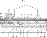
図4は本発明の第2の実施例の断面図である。本実施例と実施例1との違いは、下部電極13間にバンク8が形成されていいない点である。バンク8を形成することは、感光性のアクリル樹脂をフォトリソグラフィによってパターニングする必要があるので、工程数が増加する。また、アクリル樹脂のエッチング残渣が下部電極13上に残り、これが、有機EL層の発光特性に悪影響を与える。
FIG. 4 is a cross-sectional view of a second embodiment of the present invention. The difference between the present embodiment and the first embodiment is that the
本実施例はこのような問題を除去するために、バンク8を必要としない構成であるが、このような構成であっても、下部電極13上の透明導電膜14に対してパターニングを行わない、本発明の構成を適用することが出来る。図4において、平坦化膜12の形成までは、図1に示す実施例1と同様である。
In the present embodiment, in order to eliminate such a problem, the
平坦化膜12の上には下部電極13が形成される。下部電極13は反射率が高く、かつ、ITOとの接触抵抗が小さいAl−Ni合金が使用される。下部電極13はコンタクトホール18を介してSD配線10と接続する。SD配線10から下部電極13にデータ信号が供給され、データ信号に応じた電圧が有機EL層に印加されることによって画像が形成される。下部電極13の上には、有機EL層とコンタクトするための透明導電膜14であるITOが被着される。そして、透明導電膜14の上には複数層からなる有機EL層が形成される。図4における有機EL層は赤色有機EL層15である。有機EL層の上にはIZOからなる上部電極19が形成される。
A
図4の構造は下部電極13がアノードで上部電極19がカソードとなるトップカソード構造である。下部電極13はホールを注入する必要があるので仕事関数の比較的小さいAl合金のような金属は不適であるので、Al−Niによる下部電極13の上にITO層を被着して仕事関数を上げることによってアノードとしている。
The structure of FIG. 4 is a top cathode structure in which the
以上説明したように、本発明ではバンク8は形成されていない。バンク8を形成しない場合の問題点は図4におけるE部およびH部である。従来構造のままバンク8を形成しない場合のE部の問題点を図5に示す。図5において、平坦化膜12の上に下部電極13が形成されている。下部電極13は当該画素部分のみに形成されるのでホトリソグラフィによって、パターニングされ、エッジ部が形成されている。
As described above, the
下部電極13の上に有機EL層が蒸着される。蒸着層は総厚でも100nmから300nmと薄いため、下部電極13の端部において図5に示すような段切れを生じやすい。有機EL層層の上に上部電極19が形成される。図5に示すように、下部電極13の端部において、有機EL層が段切れを生じていると、この段切れ部において上部電極19と下部電極13がショートしてしまう。そうすると有機EL層には電圧が印加されないことになり、有機EL層は発光しない。したがって、この画素は欠陥になる。
An organic EL layer is deposited on the
バンク8を形成しない場合の他の問題点は、図4のH部である。従来構造のまま、バンク8を形成しない場合の他の問題点を図6に示す。図6はコンタクトホール部18の拡大図である。図6において、SD配線10の上にパッシベーション膜11が形成され、その上に平坦化膜12が形成されている。平坦化膜12に上には下部電極13が形成されている。下部電極13はSD配線10と接続する必要があるので、パッシベーション膜11および平坦化膜12にコンタクトホール18を形成し下部電極13とSD配線10の導通をとっている。
Another problem when the
下部電極13上に赤色有機EL層15が形成され、その上に上部電極19が形成される。ここで問題となるのは、平坦化膜12とパッシベーション膜11に形成されたコンタクトホール18は2μm以上と非常に深いのに対して、有機EL層の厚さは総厚でも100nmから300nm程度と薄いことである。したがって、図6に示すように、コンタクトホール部18において、有機EL層が段切れを起こしやすい。そうすると図6に示すように、下部電極13と上部電極19がコンタクトホール部18においてショートするという現象を生ずる。コンタクトホール部18でショートするとその画素は欠陥となる。
A red
図4に示すE部における問題点に対しては、本実施例では図4に示すように、Al−Ni合金である下部電極13の上にITOを形成している。そして、Al−Ni合金にテーパエッチングをほどこすことによって、有機EL層の端部での段切れを防止している。また、図4のH部における問題点に対しては、本実施例では、有機EL層を単色1層だけでなく、2層あるいは3層をコンタクトホール部18に被着して有機EL層の厚さを大きくすることによって段切れを防止している。
To solve the problem in the E portion shown in FIG. 4, in this embodiment, as shown in FIG. 4, ITO is formed on the
図7は図1の下部電極13付近を取り出した断面模式図である。図4と図7とではコンタクトホール18に対する下部電極13の位置が逆になっている。図7においては、ガラス基板1上にSD電極が形成された形となっているが、これは図を単純にするためであり、実際には、SD電極の下には、層間絶縁膜6、ゲート絶縁膜4、下地膜2等が存在している。
FIG. 7 is a schematic cross-sectional view of the vicinity of the
図7において、SD配線10を覆ってパッシベーション膜11、平坦化膜12が形成されている。平坦化膜12の上には下部電極13が形成されている。下部電極13はホトリソグラフィによってパターニングされている。下部電極13は平坦化膜12およびパッシベーション膜11に形成されたコンタクトホール18を介してSD電極と導通している。下部電極13の上には透明導電膜14であるITOが20nm程度の厚さに薄くスパッタリングによって被着されている。本実施例はトップカソードであるので、ITOを下部電極13として使用すれば、金属であるAl−Niは不要であるが、下部電極13の端部をテーパ形状とするために、あえて金属の下部電極13を用いている。
In FIG. 7, a
つまり、ITOでもテーパエッチングを行うことは出来る。しかしながら、ITO等の金属酸化物による透明導電膜14は硬く脆いために、テーパを形成するとそのテーパ部が破壊してしまい、結局、シャープなエッジとなってしまう。本実施例では粘りのあるAl合金を下部電極13に使用することによってテーパエッジを安定して形成することが出来る。そして、下部電極13の上にITOを薄く形成することによってアノードとしての役割を持たせている。
That is, taper etching can be performed even with ITO. However, since the transparent
ITO膜の上には赤色有機EL層15を蒸着によって形成し、その上に上部電極19をIZOによって形成する。コンタクトホール18に対応する上部電極19の上には補助電極20が形成されている。補助電極20は上部電極19の導通を補助する役割とコンタクトホール部18からの導波光の放出を防止する役割をもっている。
A red
下部電極13にはAl−Niを使用しているが、これはAi−Niの反射率が高いことのほかにITOとのコンタクト抵抗が低いという理由からである。下部電極13は次のようにして形成される。すなわち、スパッタリングによって厚さ120nmのAl−Niを形成し、ホトレジストを用いてパタンを形成し、燐酸、酢酸、硝酸の混酸を用いてエッチングする。
Al-Ni is used for the
下部電極13の端部の段差を蒸着膜である有機EL層が被覆しきれずに、下部電極13と上部電極19とがショートしてしまうことを防止するために、下部電極13の端部のテーパ角θを40度以下に保った。一般には、ジャストエッチの状態では端部にはテーパがついている。そのテーパを保つためには、エッチング後のリンスをすばやく行う必要がある。大量の水をシャワー状に吹き付けることにより、エッチング液をすばやく除去してテーパ角を保持した。
In order to prevent the
その上にスパッタリングによって厚さ20nmのITOの薄膜を形成した。放電ガスはArに対し体積比で2.5%の酸素を導入し、抵抗率が10〜300Ω・cmのITO膜に調整した。抵抗値のばらつきはかなり大きいが、有機EL層の抵抗はこれよりはるかに大きいので、この範囲であれば問題にならない。 An ITO thin film having a thickness of 20 nm was formed thereon by sputtering. The discharge gas was adjusted to an ITO film having a resistivity of 10 to 300 Ω · cm by introducing 2.5% oxygen by volume with respect to Ar. Although the variation of the resistance value is considerably large, the resistance of the organic EL layer is much larger than this, so that there is no problem within this range.
ITOは実施例1と同様、基板上の全て面に蒸着することが出来る。端子部および端子部間にITO膜が被着されても、ITO膜の厚さが5〜20nmであり、抵抗率が1〜105Ω・cmの範囲であれば、端子部における抵抗が高すぎたり、あるいは、端子部間の抵抗が小さくなって絶縁が保てないというような現象は生じない。さらに、端子間をマスクしてスパッタリングすることによってITO膜の抵抗率を0.1〜106Ω・cmの範囲に広げることが出来ることも実施例1と同様である。なお、ITOの膜厚は、より好ましくは10〜20nmである。この範囲ではITOが膜としてより安定に存在することが出来る。 As in Example 1, ITO can be deposited on all surfaces of the substrate. Even if the ITO film is deposited between the terminal parts, if the thickness of the ITO film is 5 to 20 nm and the resistivity is in the range of 1 to 10 5 Ω · cm, the resistance in the terminal part is high. There is no such phenomenon that it is too much or the resistance between the terminal portions becomes small and insulation cannot be maintained. Furthermore, it is the same as in Example 1 that the resistivity of the ITO film can be expanded to a range of 0.1 to 10 6 Ω · cm by sputtering while masking the terminals. The ITO film thickness is more preferably 10 to 20 nm. In this range, ITO can exist more stably as a film.
図7において、薄く被着したITOの上に、有機EL層としてホール輸送層、発光層、電子輸送層、電子注入層をマスク蒸着によって形成する。その後上部電極19をIZOによって形成し、補助配線20をコンタクトホール部18をカバーするように形成した。各膜は次のようにして形成する。すなわち、下部電極13となるAl−Ni層は120nm、その上のITOは20nm、ホール輸送層120nmを各色共通で形成する。その後、青色部分17は発光層を40nm、緑色部分16はホール輸送層を60nmと発光層を40nm、赤色部分15はホール輸送層を130nm、発光層30nmをそれぞれ形成する。したがって、ホール輸送層の厚さは青色部分17では120nm、緑色部分16は180nm、赤色部分15では250nmとなる。その上に各色共通で電子輸送層を10nm、電子注入層を60nm、上部電極19であるIZOを30nm被着した。
In FIG. 7, a hole transport layer, a light emitting layer, an electron transport layer, and an electron injection layer are formed as an organic EL layer on the thinly deposited ITO by mask vapor deposition. Thereafter, the
各色毎に別々に形成したホール輸送層と発光層を各色の境界部分で重なりあうように形成し、この有機EL層の重なり部21にコンタクトホール18を設ける。そうすると、コンタクトホール部18における有機EL層が厚くなり、段切れが防止されて上部電極19と下部電極13の短絡を防ぐことが出来る。赤色有機EL層15、緑色有機EL層16、青色有機EL層17の有機EL層を重ねる場合は、中間に青色有機EL層17をおくと電流が流れにくくなるので、消費電力の増加を防止することが出来る。
A hole transport layer and a light-emitting layer formed separately for each color are formed so as to overlap each other at the boundary portion of each color, and a
有機EL層を重ねた場合の断面模式図を図8に、平面図を図9に示す。図8はコンタクトホール部18において、有機EL層が重なっていることを示している。図8において、有機EL層が青色だけの場合は厚さが100nm程度であり、コンタクトホール18において容易に段切れを起こすが、3色の有機EL層が重なると総厚は600nm程度になり、段切れを生じない。ちなみに、各色の有機EL層の厚さは青色が100nm程度、緑色が200nm程度、赤色が300nm程度である。このように、3色の有機EL層を重ね合わせたことにより、有機EL層の抵抗が大きくなって、コンタクトホール18における電流が流れにくくなり、消費電力の増加を抑えることが出来る。なお、有機EL層は場所によっては3色を重ねることが出来るが、場所によっては2色のみの重なりとなる。この場合でも、1色のみの場合に比較してコンタクトホール18における段切れの危険ははるかに小さくなる。
FIG. 8 is a schematic cross-sectional view when organic EL layers are stacked, and FIG. 9 is a plan view. FIG. 8 shows that the organic EL layers overlap in the
図7にもどり、コンタクトホール部18は有機EL層を重ねても平坦にできるわけではない。コンタクトホール部18は平坦ではないために、発光層からの導波光が出射する。有機EL層からの発光のうち、上部電極19に向かう光は画像の形成に寄与する。しかし、上部電極19と平行方向に向かう光は画像形成に寄与しない。上部電極19と平行方向に向かう光を導波光と称するが、この導波光がコンタクトホール18において、屈折あるいは反射して視認されることになる。導波光は強度が強く、波長も異なるので、画質を劣化させる。この導波光を外部に出さないようにするために、コンタクトホール部18に補助配線20を設置している。
Returning to FIG. 7, the
図9は下部電極13、有機EL層等の配置を示す平面図である。図9において、下部電極13および有機EL層はモザイク状に配置されている。有機EL層は下部電極13よりも大きく形成され、コンタクトホール18が存在する部分では複数の色の有機EL層が重なっている。コンタクトホール183の部分では3色の有機EL層が重なっており、コンタクトホール182の部分では2色の有機EL層が重なっている。コンタクトホール18は金属で形成される補助配線20によって覆われている。
FIG. 9 is a plan view showing the arrangement of the
本実施例は図9のようなモザイク状の配置のみでなく、図10に示すように、ストライプ状の画素配置の場合にも適用することが出来る。図10において、コンタクトホール部18は有機EL層の重畳部21によって覆われている。そして、有機EL層の重畳部21は補助電極20によって覆われている。図10は2色分の有機EL層がコンタクトホール部18において重畳している場合である。この場合も、1色分の有機EL層に比べて、下部電極13と上部電極19がショートする確率は、はるかに小さくなる。
This embodiment can be applied not only to a mosaic arrangement as shown in FIG. 9, but also to a stripe pixel arrangement as shown in FIG. In FIG. 10, the
以上のように、本実施例では、バンク8を形成せずに、有機EL表示装置を実現することが出来る。そして、下部電極13上の透明導電膜14はパターニングをする必要がなく、薄く形成することが出来るので、優れた色純度を維持しつつ、製造歩留まりの向上、製造コストの低下を実現することが出来る。
As described above, in this embodiment, an organic EL display device can be realized without forming the
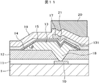
図11は本発明の第3の実施例の画素部の断面図である。本実施例も実施例2と同様バンク8を形成していない。本実施例が実施例2と異なるところは下部電極13および、下部電極13の表面被覆131である。図11において、平坦化膜12の形成までは実施例1あるいは実施例2と同様である。本実施例においては、バンク8を形成していなので、下部電極13に端部に40度以下のテーパを形成すること、コンタクトホール部18において、有機EL層を複数オーバーラップして形成する点は実施例2と同様である。
FIG. 11 is a sectional view of a pixel portion according to the third embodiment of the present invention. In this embodiment, the
本実施例においては、下部電極13にAl−Si合金を用いている。Al−Ni合金は反射率が高いのに加え、ドライエッチング残渣が少ないからである。Al−Si合金を120nm、スパッタリングによって被着し、BCl3と塩素ガスによってドライエッチングを行う。ドライエッチング条件は、10−2Paの低圧力で放電させ、反応性イオンエッチングを行う。ホトレジストとA−Siのエッチングレートをほぼ同等とすることによってレジストのテーパ角をそのままAl−Siに受け継ぐ方法で約40度のテーパ角を形成した。
In this embodiment, an Al—Si alloy is used for the
Al−Si合金と透明導電膜14のコンタクト抵抗を下げるためにAl−Siの表面の改質を行う。すなわち、2〜5wt%のZnCl2の溶液シャワーで基板を約10秒間処理し、純粋リンスすることで、Al−Si表面に極薄い表面被覆131をZnまたはZnOによって形成する。これによってコンタクト抵抗は低下し、かつ、安定化した。
In order to reduce the contact resistance between the Al—Si alloy and the transparent
その上に、透明導電膜14として、スパッタリングによって厚さ20nmのIZO薄膜を形成した。放電ガスはArに対し、体積比で2.5%の酸素を導入し、抵抗率が10〜300Ω・cmのIZO膜に調整した。抵抗値のバラつきはかなり大きいが、有機EL層の抵抗はこれよりもはるかに大きいので、この範囲であれば問題にならない。
A 20 nm thick IZO thin film was formed thereon as the transparent
本実施例のIZOは実施例1および実施例2のITOと同様、基板上の全て面に蒸着することが出来る。端子部および端子部間にIZO膜が被着されても、IZO膜の厚さが5〜20nmであり、抵抗率が1〜105Ω・cmの範囲であれば、端子部における抵抗が高すぎたり、あるいは、端子部間の抵抗が小さくなって絶縁が保てないというような現象は生じない。さらに、端子間をマスクしてスパッタリングすることによってIZO膜の抵抗率を0.1〜106Ω・cmの範囲に広げることが出来ることも実施例1と同様である。この場合も、IZOの膜厚は10〜20nmであることがより望ましい。この膜厚の範囲であれば、IZO膜が膜としてより安定に存在できるからである。 The IZO of the present embodiment can be deposited on all surfaces of the substrate in the same manner as the ITO of the first and second embodiments. Even if the IZO film is deposited between the terminal parts, if the thickness of the IZO film is 5 to 20 nm and the resistivity is in the range of 1 to 10 5 Ω · cm, the resistance in the terminal part is high. There is no such phenomenon that it is too much or the resistance between the terminal portions becomes small and insulation cannot be maintained. Further, as in Example 1, the resistivity of the IZO film can be expanded to a range of 0.1 to 10 6 Ω · cm by performing sputtering while masking the terminals. Also in this case, the film thickness of IZO is more preferably 10 to 20 nm. This is because within this thickness range, the IZO film can exist more stably as a film.
この上に有機EL層のホール輸送層、発光層、電子輸送層、電子注入層を形成し、その上に、上部電極19としてIZOを形成する。さらに補助配線をコンタクトホール18を覆うように形成する。各層の構成は次のとおりである。すなわち、下部電極13としてのAl−Si層を120nm、透明導電膜14を20nm、ホール輸送層を120nm、各層共通で形成する。
A hole transport layer, a light emitting layer, an electron transport layer, and an electron injection layer of the organic EL layer are formed thereon, and IZO is formed as the
その後、青色部分は発光層40nm、緑色部分はホール輸送層60nmと発光層40nm、赤色部分はホール輸送層130nmと発光層30nmとをそれぞれ形成する。その上に、各層共通で、電子輸送層を10nm、電子注入層を60nm、上部IZOカソードを30nm形成した。 Thereafter, the blue portion forms the light emitting layer 40 nm, the green portion forms the hole transport layer 60 nm and the light emitting layer 40 nm, and the red portion forms the hole transport layer 130 nm and the light emitting layer 30 nm. On top of that, an electron transport layer of 10 nm, an electron injection layer of 60 nm, and an upper IZO cathode of 30 nm were formed in common with each layer.
各色毎に別途形成したホール輸送層と発光層は各色の境界で重なり合うように形成し、コンタクトホール部18で、有機EL層が重なり合うようにして、コンタクトホール部18において下部電極13と上部電極19がショートしないようにした。下部電極13に正、上部電極19に負の電圧を印加することによって有機EL層は発光した。本実施例による画素配置の平面図は実施例2における図9および図10と同様である。
A hole transport layer and a light emitting layer separately formed for each color are formed so as to overlap each other at the boundary of each color, and the organic EL layer is overlapped in the
本実施例では、下部電極13としてAl−Siを用いたが、Al−Nd、あるいはAl−Cuを用いても表面にZnあるいはZnO131の薄膜を形成することが出来る。また、本実施例では、下部電極13上の透明導電膜14をIZOとしたが、これに限らず、ITOであっても同様な効果を得ることが出来る。
In this embodiment, Al—Si is used as the
以上のように、本実施例によれば、下部電極13上の透明導電膜14を基板全面に被着し、その後の透明導電膜14の加工を必要としないので、製造コストを低下させることが出来る。また、透明導電膜14の厚さが非常に薄いために、有機EL層から放出される光の色純度を劣化させることが無い。また、下部電極13と透明導電膜14を形成するIZOとのコンタクト抵抗を小さく、かつ安定化することが出来る。
As described above, according to the present embodiment, the transparent
1…ガラス基板、 2…下地膜、 3…半導体層、 4…ゲート絶縁膜、 5…ゲート配線、 6…層間絶縁膜、 8…バンク、 10…SD配線、 11…パッシベーション膜、 12…平坦化膜、 13…画素電極、 14…透明導電膜、 15…赤色有機EL層、 16…緑色有機EL層、 17…青色有機EL層、 18…コンタクトホール、 19…上部電極、 20…補助電極、 21…有機EL層の重畳部、 50…端子配線、131…表面被覆。
DESCRIPTION OF
Claims (2)
前記下部電極と前記有機EL層の間に透明導電膜を有し、
前記透明導電膜は、第1の前記下部電極と前記第1の下部電極に隣接する第2の前記下部電極との間であって、前記絶縁膜の上にも連続して形成されており、
前記透明導電膜は第1の前記端子と第2の前記端子の間にも連続膜として形成され、
前記透明導電膜は膜厚が5〜20nmであって、抵抗率が1〜10 5 Ω・cmであることを特徴とする有機EL表示装置。 A display unit is formed by forming pixels having a lower electrode, an organic EL layer, and an upper electrode in a matrix, and the lower electrode is separated by an insulating film for each pixel, and the outside of the display unit An organic EL display device having a terminal formed on
Having a transparent conductive film between the lower electrode and the organic EL layer;
The transparent conductive film is continuously formed on the insulating film between the first lower electrode and the second lower electrode adjacent to the first lower electrode ,
The transparent conductive film is also formed as a continuous film between the first terminal and the second terminal,
The organic EL display device, wherein the transparent conductive film has a thickness of 5 to 20 nm and a resistivity of 1 to 10 5 Ω · cm .
Priority Applications (2)
| Application Number | Priority Date | Filing Date | Title |
|---|---|---|---|
| JP2007229895A JP4977561B2 (en) | 2007-09-05 | 2007-09-05 | Display device |
| US12/230,768 US20090058283A1 (en) | 2007-09-05 | 2008-09-04 | Display device |
Applications Claiming Priority (1)
| Application Number | Priority Date | Filing Date | Title |
|---|---|---|---|
| JP2007229895A JP4977561B2 (en) | 2007-09-05 | 2007-09-05 | Display device |
Publications (3)
| Publication Number | Publication Date |
|---|---|
| JP2009064612A JP2009064612A (en) | 2009-03-26 |
| JP2009064612A5 JP2009064612A5 (en) | 2010-10-21 |
| JP4977561B2 true JP4977561B2 (en) | 2012-07-18 |
Family
ID=40406366
Family Applications (1)
| Application Number | Title | Priority Date | Filing Date |
|---|---|---|---|
| JP2007229895A Active JP4977561B2 (en) | 2007-09-05 | 2007-09-05 | Display device |
Country Status (2)
| Country | Link |
|---|---|
| US (1) | US20090058283A1 (en) |
| JP (1) | JP4977561B2 (en) |
Families Citing this family (16)
| Publication number | Priority date | Publication date | Assignee | Title |
|---|---|---|---|---|
| KR101570471B1 (en) * | 2008-09-18 | 2015-11-23 | 삼성디스플레이 주식회사 | Organic light emitting display and method of manufacuring the same |
| JP2010080800A (en) * | 2008-09-29 | 2010-04-08 | Seiko Instruments Inc | Light emitting device, and manufacturing method thereof |
| JP5401132B2 (en) | 2009-01-20 | 2014-01-29 | 信越ポリマー株式会社 | Radio wave transmitting decorative member and manufacturing method thereof |
| JP5346632B2 (en) * | 2009-03-17 | 2013-11-20 | 信越ポリマー株式会社 | Radio wave transmitting decorative film and decorative member using the same |
| JP5503729B2 (en) * | 2010-03-09 | 2014-05-28 | 太陽誘電株式会社 | Conductor structure, transparent device and electronic device |
| US9142598B2 (en) * | 2011-06-24 | 2015-09-22 | Semiconductor Energy Laboratory Co., Ltd. | Light-emitting panel, light-emitting device using the light-emitting panel, and method for manufacturing the light-emitting panel |
| KR101871227B1 (en) * | 2011-08-12 | 2018-08-03 | 삼성디스플레이 주식회사 | Organic light emitting device and manufacturing method therof |
| KR101970540B1 (en) * | 2012-11-15 | 2019-08-14 | 삼성디스플레이 주식회사 | Organic light emitting display device and method for fabricting the same |
| JP6155020B2 (en) * | 2012-12-21 | 2017-06-28 | 株式会社半導体エネルギー研究所 | Light emitting device and manufacturing method thereof |
| CN104157675A (en) * | 2014-08-05 | 2014-11-19 | 京东方科技集团股份有限公司 | OLED (Organic Light Emitting Diode) display device and manufacturing method thereof as well as display device |
| KR102151475B1 (en) * | 2014-09-04 | 2020-09-04 | 엘지디스플레이 주식회사 | Organic light emitting display panel and method for fabricating the same |
| KR102060471B1 (en) * | 2017-02-01 | 2019-12-30 | 엘지전자 주식회사 | Display device using semiconductor light emitting device |
| JP2018181970A (en) * | 2017-04-07 | 2018-11-15 | 株式会社ジャパンディスプレイ | Display, and method for manufacturing display |
| CN108172600B (en) * | 2017-12-29 | 2020-01-17 | 深圳市华星光电半导体显示技术有限公司 | Color film substrate for WOLED display and WOLED display |
| KR20200066959A (en) * | 2018-12-03 | 2020-06-11 | 엘지디스플레이 주식회사 | Transparent Display Device |
| US11380864B2 (en) * | 2019-02-13 | 2022-07-05 | Canon Kabushiki Kaisha | Electronic device, display apparatus, photoelectric conversion apparatus, electronic apparatus, illumination apparatus, and moving object |
Family Cites Families (6)
| Publication number | Priority date | Publication date | Assignee | Title |
|---|---|---|---|---|
| US6956324B2 (en) * | 2000-08-04 | 2005-10-18 | Semiconductor Energy Laboratory Co., Ltd. | Semiconductor device and manufacturing method therefor |
| JP3708916B2 (en) * | 2001-08-24 | 2005-10-19 | 株式会社半導体エネルギー研究所 | Light emitting device |
| JP4089544B2 (en) * | 2002-12-11 | 2008-05-28 | ソニー株式会社 | Display device and manufacturing method of display device |
| JP2005197009A (en) * | 2003-12-26 | 2005-07-21 | Sanyo Electric Co Ltd | Manufacturing method and manufacturing device of display device |
| JP4555727B2 (en) * | 2005-04-22 | 2010-10-06 | 株式会社 日立ディスプレイズ | Organic light emitting display |
| JP5007170B2 (en) * | 2007-07-20 | 2012-08-22 | 株式会社ジャパンディスプレイイースト | Organic EL display device |
-
2007
- 2007-09-05 JP JP2007229895A patent/JP4977561B2/en active Active
-
2008
- 2008-09-04 US US12/230,768 patent/US20090058283A1/en not_active Abandoned
Also Published As
| Publication number | Publication date |
|---|---|
| US20090058283A1 (en) | 2009-03-05 |
| JP2009064612A (en) | 2009-03-26 |
Similar Documents
| Publication | Publication Date | Title |
|---|---|---|
| JP4977561B2 (en) | Display device | |
| JP2009058897A (en) | Display device | |
| US10096662B2 (en) | Organic light emitting display device including a tandem structure and method of manufacturing the organic light emitting display device including the tandem structure | |
| US8212258B2 (en) | Display device and method for manufacturing display device | |
| US10734461B2 (en) | Thin film transistor array panel and organic light emitting diode display including the same | |
| US10727292B2 (en) | OLED with buffer layer over emitting layer | |
| KR100667081B1 (en) | Organic light emitting display device and the methode for fabricating the same | |
| CN109980122B (en) | Electroluminescent display device | |
| JP2008124316A (en) | Organic el display | |
| JP2005056846A (en) | Organic electroluminescence device and its manufacturing method | |
| JP4165145B2 (en) | Organic light emitting display | |
| JP2008130363A (en) | Organic el element, its manufacturing method, organic el display, and its manufacturing method | |
| JP2010062233A (en) | Display apparatus | |
| JP5007170B2 (en) | Organic EL display device | |
| KR20220129601A (en) | ORGANIC LIGHT-EMITTING DIODE (OLED) display devices with mirror and method for manufacturing the same | |
| JP2011048973A (en) | Organic el display device | |
| JP2011034931A (en) | Organic el display device | |
| JP2006164737A (en) | Display element or display panel equipped with it and display device | |
| US20240122033A1 (en) | Display device and manufacturing method of the same | |
| US20240121994A1 (en) | Display device and manufacturing method of the same | |
| JP2019133835A (en) | Organic el display panel and method for manufacturing the same | |
| JP5642841B2 (en) | ORGANIC EL ELEMENT OR DISPLAY PANEL AND DISPLAY DEVICE PROVIDED WITH SAME | |
| US11588129B2 (en) | Organic light-emitting diode display device and manufacturing method thereof | |
| JP2008198491A (en) | Organic el display panel and its manufacturing method | |
| JP5427253B2 (en) | ORGANIC EL ELEMENT OR DISPLAY PANEL AND DISPLAY DEVICE PROVIDED WITH SAME |
Legal Events
| Date | Code | Title | Description |
|---|---|---|---|
| A521 | Request for written amendment filed |
Free format text: JAPANESE INTERMEDIATE CODE: A523 Effective date: 20100903 |
|
| A621 | Written request for application examination |
Free format text: JAPANESE INTERMEDIATE CODE: A621 Effective date: 20100903 |
|
| A711 | Notification of change in applicant |
Free format text: JAPANESE INTERMEDIATE CODE: A712 Effective date: 20110218 |
|
| RD03 | Notification of appointment of power of attorney |
Free format text: JAPANESE INTERMEDIATE CODE: A7423 Effective date: 20110218 |
|
| A977 | Report on retrieval |
Free format text: JAPANESE INTERMEDIATE CODE: A971007 Effective date: 20111227 |
|
| A131 | Notification of reasons for refusal |
Free format text: JAPANESE INTERMEDIATE CODE: A131 Effective date: 20120105 |
|
| A521 | Request for written amendment filed |
Free format text: JAPANESE INTERMEDIATE CODE: A523 Effective date: 20120227 |
|
| TRDD | Decision of grant or rejection written | ||
| A01 | Written decision to grant a patent or to grant a registration (utility model) |
Free format text: JAPANESE INTERMEDIATE CODE: A01 Effective date: 20120321 |
|
| A01 | Written decision to grant a patent or to grant a registration (utility model) |
Free format text: JAPANESE INTERMEDIATE CODE: A01 |
|
| A61 | First payment of annual fees (during grant procedure) |
Free format text: JAPANESE INTERMEDIATE CODE: A61 Effective date: 20120416 |
|
| R150 | Certificate of patent or registration of utility model |
Ref document number: 4977561 Country of ref document: JP Free format text: JAPANESE INTERMEDIATE CODE: R150 Free format text: JAPANESE INTERMEDIATE CODE: R150 |
|
| FPAY | Renewal fee payment (event date is renewal date of database) |
Free format text: PAYMENT UNTIL: 20150420 Year of fee payment: 3 |
|
| R250 | Receipt of annual fees |
Free format text: JAPANESE INTERMEDIATE CODE: R250 |
|
| R250 | Receipt of annual fees |
Free format text: JAPANESE INTERMEDIATE CODE: R250 |
|
| R250 | Receipt of annual fees |
Free format text: JAPANESE INTERMEDIATE CODE: R250 |
|
| R250 | Receipt of annual fees |
Free format text: JAPANESE INTERMEDIATE CODE: R250 |
|
| S531 | Written request for registration of change of domicile |
Free format text: JAPANESE INTERMEDIATE CODE: R313531 |
|
| S533 | Written request for registration of change of name |
Free format text: JAPANESE INTERMEDIATE CODE: R313533 |
|
| S111 | Request for change of ownership or part of ownership |
Free format text: JAPANESE INTERMEDIATE CODE: R313113 |
|
| R350 | Written notification of registration of transfer |
Free format text: JAPANESE INTERMEDIATE CODE: R350 |
|
| R350 | Written notification of registration of transfer |
Free format text: JAPANESE INTERMEDIATE CODE: R350 |
|
| R250 | Receipt of annual fees |
Free format text: JAPANESE INTERMEDIATE CODE: R250 |
|
| R250 | Receipt of annual fees |
Free format text: JAPANESE INTERMEDIATE CODE: R250 |
|
| R250 | Receipt of annual fees |
Free format text: JAPANESE INTERMEDIATE CODE: R250 |
|
| R250 | Receipt of annual fees |
Free format text: JAPANESE INTERMEDIATE CODE: R250 |
|
| R250 | Receipt of annual fees |
Free format text: JAPANESE INTERMEDIATE CODE: R250 |
|
| R250 | Receipt of annual fees |
Free format text: JAPANESE INTERMEDIATE CODE: R250 |