JP4977181B2 - 固体撮像装置およびその製造方法 - Google Patents
固体撮像装置およびその製造方法 Download PDFInfo
- Publication number
- JP4977181B2 JP4977181B2 JP2009186040A JP2009186040A JP4977181B2 JP 4977181 B2 JP4977181 B2 JP 4977181B2 JP 2009186040 A JP2009186040 A JP 2009186040A JP 2009186040 A JP2009186040 A JP 2009186040A JP 4977181 B2 JP4977181 B2 JP 4977181B2
- Authority
- JP
- Japan
- Prior art keywords
- conductivity type
- semiconductor layer
- element isolation
- type semiconductor
- layer
- Prior art date
- Legal status (The legal status is an assumption and is not a legal conclusion. Google has not performed a legal analysis and makes no representation as to the accuracy of the status listed.)
- Expired - Fee Related
Links
Images


Classifications
-
- H—ELECTRICITY
- H01—ELECTRIC ELEMENTS
- H01L—SEMICONDUCTOR DEVICES NOT COVERED BY CLASS H10
- H01L21/00—Processes or apparatus adapted for the manufacture or treatment of semiconductor or solid state devices or of parts thereof
- H01L21/02—Manufacture or treatment of semiconductor devices or of parts thereof
- H01L21/04—Manufacture or treatment of semiconductor devices or of parts thereof the devices having potential barriers, e.g. a PN junction, depletion layer or carrier concentration layer
- H01L21/18—Manufacture or treatment of semiconductor devices or of parts thereof the devices having potential barriers, e.g. a PN junction, depletion layer or carrier concentration layer the devices having semiconductor bodies comprising elements of Group IV of the Periodic Table or AIIIBV compounds with or without impurities, e.g. doping materials
- H01L21/26—Bombardment with radiation
- H01L21/263—Bombardment with radiation with high-energy radiation
- H01L21/265—Bombardment with radiation with high-energy radiation producing ion implantation
- H01L21/26506—Bombardment with radiation with high-energy radiation producing ion implantation in group IV semiconductors
- H01L21/26513—Bombardment with radiation with high-energy radiation producing ion implantation in group IV semiconductors of electrically active species
- H01L21/2652—Through-implantation
-
- H—ELECTRICITY
- H10—SEMICONDUCTOR DEVICES; ELECTRIC SOLID-STATE DEVICES NOT OTHERWISE PROVIDED FOR
- H10F—INORGANIC SEMICONDUCTOR DEVICES SENSITIVE TO INFRARED RADIATION, LIGHT, ELECTROMAGNETIC RADIATION OF SHORTER WAVELENGTH OR CORPUSCULAR RADIATION
- H10F39/00—Integrated devices, or assemblies of multiple devices, comprising at least one element covered by group H10F30/00, e.g. radiation detectors comprising photodiode arrays
- H10F39/011—Manufacture or treatment of image sensors covered by group H10F39/12
- H10F39/014—Manufacture or treatment of image sensors covered by group H10F39/12 of CMOS image sensors
-
- H—ELECTRICITY
- H10—SEMICONDUCTOR DEVICES; ELECTRIC SOLID-STATE DEVICES NOT OTHERWISE PROVIDED FOR
- H10F—INORGANIC SEMICONDUCTOR DEVICES SENSITIVE TO INFRARED RADIATION, LIGHT, ELECTROMAGNETIC RADIATION OF SHORTER WAVELENGTH OR CORPUSCULAR RADIATION
- H10F39/00—Integrated devices, or assemblies of multiple devices, comprising at least one element covered by group H10F30/00, e.g. radiation detectors comprising photodiode arrays
- H10F39/80—Constructional details of image sensors
- H10F39/807—Pixel isolation structures
Landscapes
- Physics & Mathematics (AREA)
- Engineering & Computer Science (AREA)
- High Energy & Nuclear Physics (AREA)
- General Physics & Mathematics (AREA)
- Toxicology (AREA)
- Condensed Matter Physics & Semiconductors (AREA)
- Health & Medical Sciences (AREA)
- Manufacturing & Machinery (AREA)
- Computer Hardware Design (AREA)
- Microelectronics & Electronic Packaging (AREA)
- Power Engineering (AREA)
- Solid State Image Pick-Up Elements (AREA)
- Element Separation (AREA)
Description
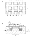
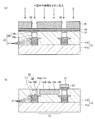
また、本願発明の一態様によれば、第1導電型の半導体層と、前記第1導電型の半導体層上に設けられた第2導電型の半導体層と、前記第2導電型の半導体層中に形成された受光素子と、前記受光素子を前記第2導電型の半導体層の面内方向において取り囲むように形成された素子分離領域とを備え、前記素子分離領域は、前記第1導電型の半導体層に接続された第1導電型の第1の素子分離部と、前記第1の素子分離部上に形成された空洞と、前記空洞上に形成された第1導電型の第2の素子分離部とを有し、前記第1の素子分離部は、前記第2導電型の半導体層の表層側の素子分離幅が前記第1導電型の半導体層側の素子分離幅よりも大きいこと、を特徴とする固体撮像装置が提供される。

Claims (8)
- 第1導電型の半導体層と、
前記第1導電型の半導体層上に設けられた第2導電型の半導体層と、
前記第2導電型の半導体層中に形成された受光素子と、
前記受光素子を前記第2導電型の半導体層の面内方向において取り囲むように形成された素子分離領域とを備え、
前記素子分離領域は、前記第1導電型の半導体層に接続された第1導電型の第1の素子分離部と、前記第1の素子分離部上に形成された空洞と、前記空洞上に形成された第1導電型の第2の素子分離部とを有し、
前記第1の素子分離部は、前記第2導電型の半導体層の表層側の不純物濃度が前記第1導電型の半導体層側の不純物濃度よりも高いこと、
を特徴とする固体撮像装置。 - 第1導電型の半導体層と、
前記第1導電型の半導体層上に設けられた第2導電型の半導体層と、
前記第2導電型の半導体層中に形成された受光素子と、
前記受光素子を前記第2導電型の半導体層の面内方向において取り囲むように形成された素子分離領域とを備え、
前記素子分離領域は、前記第1導電型の半導体層に接続された第1導電型の第1の素子分離部と、前記第1の素子分離部上に形成された空洞と、前記空洞上に形成された第1導電型の第2の素子分離部とを有し、
前記第1の素子分離部は、前記第2導電型の半導体層の表層側の素子分離幅が前記第1導電型の半導体層側の素子分離幅よりも大きいこと、
を特徴とする固体撮像装置。 - 前記受光素子は電荷蓄積層を有しており、前記空洞の底部の深さ位置は前記電荷蓄積層の下端部の深さよりも同等以上の深い位置であること、
を特徴とする請求項1または2に記載の固体撮像装置。 - 前記第2導電型の半導体層の表面からの前記空洞の底部の深さが、青色光の波長よりも深く緑色光の波長よりも浅いこと、
を特徴とする請求項1〜3のいずれか1つに記載の固体撮像装置。 - 前記第2導電型の半導体層の表面からの前記空洞の底部の深さが、320nm〜790nmであること、
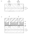
を特徴とする請求項1〜3のいずれか1つに記載の固体撮像装置。 - 第1導電型の半導体層上に第2導電型の半導体層を形成する工程と、
前記第2導電型の半導体層の所定の領域を前記第2導電型の半導体層の面内方向において取り囲むように開口を形成する工程と、
前記第2導電型の半導体層に非酸化性雰囲気中で熱処理を施すことにより前記開口を封止して空洞を形成する工程と、
前記空洞に対応する領域が開口されたパターンを前記第2導電型の半導体層上に形成する工程と
前記パターンをマスクとして前記第2導電型の半導体層に第1導電型イオンをイオン注入して素子分離部を形成する工程と、
前記第2導電型の半導体層の面内方向において前記素子分離部及び前記空洞に取り囲まれた前記第2導電型の半導体層に受光素子を形成する工程と、
を備えることを特徴とする固体撮像装置の製造方法。 - 素子分離部の形成工程は、前記空洞の下部の前記第2導電型の半導体層中にイオンの注入深さを変えて第1導電型イオンの注入を複数回行うことを特徴とする請求項6に記載の固体撮像装置の製造方法。
- 前記開口の深さが、320nm〜790nmであること、
を特徴とする請求項6に記載の固体撮像装置の製造方法。
Priority Applications (2)
| Application Number | Priority Date | Filing Date | Title |
|---|---|---|---|
| JP2009186040A JP4977181B2 (ja) | 2009-08-10 | 2009-08-10 | 固体撮像装置およびその製造方法 |
| US12/722,716 US20110031576A1 (en) | 2009-08-10 | 2010-03-12 | Solid-state imaging device and manufacturing method thereof |
Applications Claiming Priority (1)
| Application Number | Priority Date | Filing Date | Title |
|---|---|---|---|
| JP2009186040A JP4977181B2 (ja) | 2009-08-10 | 2009-08-10 | 固体撮像装置およびその製造方法 |
Publications (2)
| Publication Number | Publication Date |
|---|---|
| JP2011040543A JP2011040543A (ja) | 2011-02-24 |
| JP4977181B2 true JP4977181B2 (ja) | 2012-07-18 |
Family
ID=43534173
Family Applications (1)
| Application Number | Title | Priority Date | Filing Date |
|---|---|---|---|
| JP2009186040A Expired - Fee Related JP4977181B2 (ja) | 2009-08-10 | 2009-08-10 | 固体撮像装置およびその製造方法 |
Country Status (2)
| Country | Link |
|---|---|
| US (1) | US20110031576A1 (ja) |
| JP (1) | JP4977181B2 (ja) |
Families Citing this family (11)
| Publication number | Priority date | Publication date | Assignee | Title |
|---|---|---|---|---|
| US8951826B2 (en) * | 2012-01-31 | 2015-02-10 | Taiwan Semiconductor Manufacturing Company, Ltd. | Method for increasing photodiode full well capacity |
| JP2014093482A (ja) | 2012-11-06 | 2014-05-19 | Toshiba Corp | 固体撮像装置の製造方法および固体撮像装置 |
| JP6278608B2 (ja) | 2013-04-08 | 2018-02-14 | キヤノン株式会社 | 半導体装置およびその製造方法 |
| JP2015056622A (ja) * | 2013-09-13 | 2015-03-23 | 株式会社リコー | 半導体装置 |
| US9647022B2 (en) * | 2015-02-12 | 2017-05-09 | Taiwan Semiconductor Manufacturing Co., Ltd. | Multi-layer structure for high aspect ratio etch |
| JP2017045873A (ja) * | 2015-08-27 | 2017-03-02 | ルネサスエレクトロニクス株式会社 | 半導体装置の製造方法および半導体装置 |
| US10433168B2 (en) * | 2015-12-22 | 2019-10-01 | Quanta Computer Inc. | Method and system for combination wireless and smartcard authorization |
| US9780250B2 (en) * | 2016-01-14 | 2017-10-03 | Varian Semiconductor Equipment Associates, Inc. | Self-aligned mask for ion implantation |
| JP6688165B2 (ja) | 2016-06-10 | 2020-04-28 | キヤノン株式会社 | 撮像装置及び撮像システム |
| JP7013119B2 (ja) | 2016-07-21 | 2022-01-31 | キヤノン株式会社 | 固体撮像素子、固体撮像素子の製造方法、及び撮像システム |
| CN108539016B (zh) | 2018-03-29 | 2022-01-25 | 京东方科技集团股份有限公司 | 柔性衬底及其制备方法、显示面板的制备方法和显示装置 |
Family Cites Families (13)
| Publication number | Priority date | Publication date | Assignee | Title |
|---|---|---|---|---|
| JPS5197988A (en) * | 1975-02-25 | 1976-08-28 | Handotaisochino seizohoho | |
| JP4074051B2 (ja) * | 1999-08-31 | 2008-04-09 | 株式会社東芝 | 半導体基板およびその製造方法 |
| US7091536B2 (en) * | 2002-11-14 | 2006-08-15 | Micron Technology, Inc. | Isolation process and structure for CMOS imagers |
| JP2004228407A (ja) * | 2003-01-24 | 2004-08-12 | Sony Corp | 固体撮像素子および固体撮像素子の製造方法 |
| JP4718875B2 (ja) * | 2005-03-31 | 2011-07-06 | 株式会社東芝 | 固体撮像素子 |
| KR100688547B1 (ko) * | 2005-05-18 | 2007-03-02 | 삼성전자주식회사 | Sti 구조를 가지는 반도체 소자 및 그 제조 방법 |
| US7800146B2 (en) * | 2005-08-26 | 2010-09-21 | Aptina Imaging Corporation | Implanted isolation region for imager pixels |
| JP2007227761A (ja) * | 2006-02-24 | 2007-09-06 | Matsushita Electric Ind Co Ltd | 固体撮像装置用素子 |
| JP2008078302A (ja) * | 2006-09-20 | 2008-04-03 | Canon Inc | 撮像装置および撮像システム |
| JP2008084962A (ja) * | 2006-09-26 | 2008-04-10 | Toshiba Corp | 固体撮像装置及びその製造方法 |
| JP4960058B2 (ja) * | 2006-10-04 | 2012-06-27 | 株式会社東芝 | 増幅型固体撮像素子 |
| KR100843965B1 (ko) * | 2007-03-19 | 2008-07-03 | 동부일렉트로닉스 주식회사 | 이미지센서 및 그 제조방법 |
| US7800192B2 (en) * | 2008-02-08 | 2010-09-21 | Omnivision Technologies, Inc. | Backside illuminated image sensor having deep light reflective trenches |
-
2009
- 2009-08-10 JP JP2009186040A patent/JP4977181B2/ja not_active Expired - Fee Related
-
2010
- 2010-03-12 US US12/722,716 patent/US20110031576A1/en not_active Abandoned
Also Published As
| Publication number | Publication date |
|---|---|
| US20110031576A1 (en) | 2011-02-10 |
| JP2011040543A (ja) | 2011-02-24 |
Similar Documents
| Publication | Publication Date | Title |
|---|---|---|
| JP4977181B2 (ja) | 固体撮像装置およびその製造方法 | |
| CN103403869B (zh) | 固态成像装置、固态成像装置的制造方法和电子设备 | |
| JP5318955B2 (ja) | 空隙を有する浅型トレンチ分離構造と、これを使用するcmos画像センサと、cmos画像センサの製造方法 | |
| TWI864354B (zh) | 具有鈍化全深溝槽隔離的影像感測器及相關聯的製造方法與降低影像感測器中的雜訊方法 | |
| DE102015109641B4 (de) | Implantatsschadenfreier Bildsensor und diesbezügliches Verfahren | |
| CN100485947C (zh) | 互补金属氧化物半导体图像传感器及其制造方法 | |
| JP7009684B2 (ja) | 近赤外線cmosセンサの製造方法 | |
| US12211877B2 (en) | Back-side deep trench isolation structure for image sensor | |
| US10269864B2 (en) | Pixel isolation device and fabrication method | |
| JP6302216B2 (ja) | 半導体装置およびその製造方法 | |
| US8440540B2 (en) | Method for doping a selected portion of a device | |
| US8178913B2 (en) | Semiconductor device and method for manufacturing same | |
| US11282890B2 (en) | Shallow trench isolation (STI) structure for suppressing dark current and method of forming | |
| US8987033B2 (en) | Method for forming CMOS image sensors | |
| CN101512752A (zh) | 在浅沟槽隔离拐角处的注入 | |
| JP2009194269A (ja) | 固体撮像装置およびその製造方法 | |
| JP2010103318A (ja) | 半導体基板およびその製造方法、固体撮像素子 | |
| KR100606914B1 (ko) | 반도체 소자의 격리영역 형성방법 | |
| JP4768889B1 (ja) | 画像撮像デバイス及びその製造方法 | |
| JP2010251628A (ja) | 固体撮像装置およびその製造方法 | |
| KR100729742B1 (ko) | 이미지 센서의 제조방법 | |
| JP2008300537A (ja) | 固体撮像装置 | |
| CN114709229A (zh) | 集成芯片及其形成方法 | |
| CN113838880B (zh) | 一种cis芯片异形栅极结构及制作方法 | |
| CN109860215B (zh) | 图像传感器及其形成方法 |
Legal Events
| Date | Code | Title | Description |
|---|---|---|---|
| A621 | Written request for application examination |
Free format text: JAPANESE INTERMEDIATE CODE: A621 Effective date: 20110802 |
|
| A977 | Report on retrieval |
Free format text: JAPANESE INTERMEDIATE CODE: A971007 Effective date: 20111226 |
|
| A131 | Notification of reasons for refusal |
Free format text: JAPANESE INTERMEDIATE CODE: A131 Effective date: 20120104 |
|
| A521 | Request for written amendment filed |
Free format text: JAPANESE INTERMEDIATE CODE: A523 Effective date: 20120301 |
|
| TRDD | Decision of grant or rejection written | ||
| A01 | Written decision to grant a patent or to grant a registration (utility model) |
Free format text: JAPANESE INTERMEDIATE CODE: A01 Effective date: 20120321 |
|
| A01 | Written decision to grant a patent or to grant a registration (utility model) |
Free format text: JAPANESE INTERMEDIATE CODE: A01 |
|
| A61 | First payment of annual fees (during grant procedure) |
Free format text: JAPANESE INTERMEDIATE CODE: A61 Effective date: 20120413 |
|
| FPAY | Renewal fee payment (event date is renewal date of database) |
Free format text: PAYMENT UNTIL: 20150420 Year of fee payment: 3 |
|
| LAPS | Cancellation because of no payment of annual fees |