JP4922581B2 - スパッタリング装置及びスパッタリング方法 - Google Patents
スパッタリング装置及びスパッタリング方法 Download PDFInfo
- Publication number
- JP4922581B2 JP4922581B2 JP2005220889A JP2005220889A JP4922581B2 JP 4922581 B2 JP4922581 B2 JP 4922581B2 JP 2005220889 A JP2005220889 A JP 2005220889A JP 2005220889 A JP2005220889 A JP 2005220889A JP 4922581 B2 JP4922581 B2 JP 4922581B2
- Authority
- JP
- Japan
- Prior art keywords
- targets
- target
- substrate
- sputtering
- film
- Prior art date
- Legal status (The legal status is an assumption and is not a legal conclusion. Google has not performed a legal analysis and makes no representation as to the accuracy of the status listed.)
- Active
Links
- 238000004544 sputter deposition Methods 0.000 title claims description 39
- 239000000758 substrate Substances 0.000 claims description 39
- 230000004907 flux Effects 0.000 claims description 20
- 238000000429 assembly Methods 0.000 claims description 6
- 230000000712 assembly Effects 0.000 claims description 6
- 239000010408 film Substances 0.000 description 54
- 239000007789 gas Substances 0.000 description 34
- 230000015572 biosynthetic process Effects 0.000 description 20
- 238000012546 transfer Methods 0.000 description 11
- 230000002159 abnormal effect Effects 0.000 description 8
- 238000000034 method Methods 0.000 description 7
- 230000002093 peripheral effect Effects 0.000 description 7
- 238000005546 reactive sputtering Methods 0.000 description 7
- 230000000052 comparative effect Effects 0.000 description 5
- 239000002245 particle Substances 0.000 description 5
- XKRFYHLGVUSROY-UHFFFAOYSA-N Argon Chemical compound [Ar] XKRFYHLGVUSROY-UHFFFAOYSA-N 0.000 description 4
- 238000010586 diagram Methods 0.000 description 3
- 238000001755 magnetron sputter deposition Methods 0.000 description 3
- 238000005192 partition Methods 0.000 description 3
- 239000012495 reaction gas Substances 0.000 description 3
- 238000000137 annealing Methods 0.000 description 2
- 229910052786 argon Inorganic materials 0.000 description 2
- 238000009826 distribution Methods 0.000 description 2
- 230000000694 effects Effects 0.000 description 2
- 238000010891 electric arc Methods 0.000 description 2
- 230000003628 erosive effect Effects 0.000 description 2
- 230000005415 magnetization Effects 0.000 description 2
- 229910000838 Al alloy Inorganic materials 0.000 description 1
- 229910006404 SnO 2 Inorganic materials 0.000 description 1
- 238000001816 cooling Methods 0.000 description 1
- 238000012937 correction Methods 0.000 description 1
- 230000003247 decreasing effect Effects 0.000 description 1
- 238000000151 deposition Methods 0.000 description 1
- 230000008021 deposition Effects 0.000 description 1
- 230000005684 electric field Effects 0.000 description 1
- 239000011521 glass Substances 0.000 description 1
- 150000002500 ions Chemical class 0.000 description 1
- 230000009191 jumping Effects 0.000 description 1
- 238000004519 manufacturing process Methods 0.000 description 1
- 239000000463 material Substances 0.000 description 1
- 238000005259 measurement Methods 0.000 description 1
- 239000000203 mixture Substances 0.000 description 1
- 238000012544 monitoring process Methods 0.000 description 1
- 239000010409 thin film Substances 0.000 description 1
- 230000032258 transport Effects 0.000 description 1
Images


Classifications
-
- C—CHEMISTRY; METALLURGY
- C23—COATING METALLIC MATERIAL; COATING MATERIAL WITH METALLIC MATERIAL; CHEMICAL SURFACE TREATMENT; DIFFUSION TREATMENT OF METALLIC MATERIAL; COATING BY VACUUM EVAPORATION, BY SPUTTERING, BY ION IMPLANTATION OR BY CHEMICAL VAPOUR DEPOSITION, IN GENERAL; INHIBITING CORROSION OF METALLIC MATERIAL OR INCRUSTATION IN GENERAL
- C23C—COATING METALLIC MATERIAL; COATING MATERIAL WITH METALLIC MATERIAL; SURFACE TREATMENT OF METALLIC MATERIAL BY DIFFUSION INTO THE SURFACE, BY CHEMICAL CONVERSION OR SUBSTITUTION; COATING BY VACUUM EVAPORATION, BY SPUTTERING, BY ION IMPLANTATION OR BY CHEMICAL VAPOUR DEPOSITION, IN GENERAL
- C23C14/00—Coating by vacuum evaporation, by sputtering or by ion implantation of the coating forming material
- C23C14/22—Coating by vacuum evaporation, by sputtering or by ion implantation of the coating forming material characterised by the process of coating
- C23C14/34—Sputtering
- C23C14/35—Sputtering by application of a magnetic field, e.g. magnetron sputtering
- C23C14/352—Sputtering by application of a magnetic field, e.g. magnetron sputtering using more than one target
-
- C—CHEMISTRY; METALLURGY
- C23—COATING METALLIC MATERIAL; COATING MATERIAL WITH METALLIC MATERIAL; CHEMICAL SURFACE TREATMENT; DIFFUSION TREATMENT OF METALLIC MATERIAL; COATING BY VACUUM EVAPORATION, BY SPUTTERING, BY ION IMPLANTATION OR BY CHEMICAL VAPOUR DEPOSITION, IN GENERAL; INHIBITING CORROSION OF METALLIC MATERIAL OR INCRUSTATION IN GENERAL
- C23C—COATING METALLIC MATERIAL; COATING MATERIAL WITH METALLIC MATERIAL; SURFACE TREATMENT OF METALLIC MATERIAL BY DIFFUSION INTO THE SURFACE, BY CHEMICAL CONVERSION OR SUBSTITUTION; COATING BY VACUUM EVAPORATION, BY SPUTTERING, BY ION IMPLANTATION OR BY CHEMICAL VAPOUR DEPOSITION, IN GENERAL
- C23C14/00—Coating by vacuum evaporation, by sputtering or by ion implantation of the coating forming material
- C23C14/0021—Reactive sputtering or evaporation
- C23C14/0036—Reactive sputtering
Landscapes
- Chemical & Material Sciences (AREA)
- Chemical Kinetics & Catalysis (AREA)
- Engineering & Computer Science (AREA)
- Materials Engineering (AREA)
- Mechanical Engineering (AREA)
- Metallurgy (AREA)
- Organic Chemistry (AREA)
- Physical Vapour Deposition (AREA)
Description
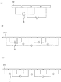
244 磁石組立体 250 駆動軸
251 ボールネジ E1〜E3 交流電源
S 基板
Claims (4)
- 真空チャンバー内に所定の間隔を置いて並設した少なくとも4枚以上のターゲットと、並設されたターゲットのうち2枚のターゲットに対して負電位及び正電位又は接地電位を交互に印加する交流電源とを備え、各交流電源を相互に隣接しない2枚のターゲットに接続したことを特徴とするスパッタリング装置。
- 各ターゲットの前方に磁束を形成するように各ターゲットの後方に配置された複数の磁石から構成される磁石組立体と、磁束がターゲットに対して平行移動するようにこれらの磁石組立体を駆動する駆動手段とを備えることを特徴とする請求項1に記載のスパッタリング装置。
- 前記磁石組立体を各ターゲット後方にそれぞれ配置した場合に、各磁石組立体によって形成される磁束の密度を略均一にする磁束密度補正手段を備えたことを特徴とする請求項1又は2に記載のスパッタリング装置。
- 真空チャンバー内に所定の間隔を置いて並設された少なくとも4枚以上のターゲットに対向する位置に基板を搬送し、並設されたターゲットのうち相互に隣接しない2枚のターゲットに対して負電位及び正電位又は接地電位を交互に印加して、ターゲット上にプラズマを発生させて基板上に膜を形成することを特徴とするスパッタリング方法。
Priority Applications (4)
| Application Number | Priority Date | Filing Date | Title |
|---|---|---|---|
| JP2005220889A JP4922581B2 (ja) | 2005-07-29 | 2005-07-29 | スパッタリング装置及びスパッタリング方法 |
| TW095125494A TWI401333B (zh) | 2005-07-29 | 2006-07-12 | Sputtering apparatus and sputtering method |
| KR1020060069713A KR101231668B1 (ko) | 2005-07-29 | 2006-07-25 | 스퍼터링 장치 및 스퍼터링 방법 |
| CN2006101076272A CN1904132B (zh) | 2005-07-29 | 2006-07-28 | 溅射装置和溅射方法 |
Applications Claiming Priority (1)
| Application Number | Priority Date | Filing Date | Title |
|---|---|---|---|
| JP2005220889A JP4922581B2 (ja) | 2005-07-29 | 2005-07-29 | スパッタリング装置及びスパッタリング方法 |
Publications (3)
| Publication Number | Publication Date |
|---|---|
| JP2007031817A JP2007031817A (ja) | 2007-02-08 |
| JP2007031817A5 JP2007031817A5 (ja) | 2008-08-21 |
| JP4922581B2 true JP4922581B2 (ja) | 2012-04-25 |
Family
ID=37673492
Family Applications (1)
| Application Number | Title | Priority Date | Filing Date |
|---|---|---|---|
| JP2005220889A Active JP4922581B2 (ja) | 2005-07-29 | 2005-07-29 | スパッタリング装置及びスパッタリング方法 |
Country Status (4)
| Country | Link |
|---|---|
| JP (1) | JP4922581B2 (ja) |
| KR (1) | KR101231668B1 (ja) |
| CN (1) | CN1904132B (ja) |
| TW (1) | TWI401333B (ja) |
Families Citing this family (12)
| Publication number | Priority date | Publication date | Assignee | Title |
|---|---|---|---|---|
| CN101622374B (zh) * | 2007-03-01 | 2012-07-18 | 株式会社爱发科 | 薄膜形成方法及薄膜形成装置 |
| JP4707693B2 (ja) * | 2007-05-01 | 2011-06-22 | 株式会社アルバック | スパッタリング装置及びスパッタリング方法 |
| JP2009024230A (ja) * | 2007-07-20 | 2009-02-05 | Kobe Steel Ltd | スパッタリング装置 |
| WO2009025306A1 (ja) * | 2007-08-20 | 2009-02-26 | Ulvac, Inc. | スパッタリング方法 |
| WO2010090197A1 (ja) * | 2009-02-04 | 2010-08-12 | シャープ株式会社 | 透明導電膜形成体及びその製造方法 |
| WO2011031056A2 (ko) * | 2009-09-09 | 2011-03-17 | 주식회사 티엔텍 | 기판진동장치가 구비된 스퍼터링 시스템 및 그 제어방법 |
| CN102312206B (zh) * | 2010-06-29 | 2015-07-15 | 株式会社爱发科 | 溅射方法 |
| CN103827347B (zh) * | 2011-08-25 | 2016-06-22 | 应用材料公司 | 溅射装置与方法 |
| CN103014639B (zh) * | 2012-12-12 | 2015-02-25 | 京东方科技集团股份有限公司 | 溅射靶材及溅射装置 |
| CN104878356B (zh) * | 2015-06-08 | 2017-11-24 | 光驰科技(上海)有限公司 | 一种磁控溅射靶材磁铁放置角度的确定方法 |
| KR102580293B1 (ko) * | 2016-01-05 | 2023-09-19 | 삼성디스플레이 주식회사 | 스퍼터링 장치 |
| JP2020143356A (ja) * | 2019-03-08 | 2020-09-10 | 株式会社アルバック | スパッタリング装置及びスパッタリング方法 |
Family Cites Families (9)
| Publication number | Priority date | Publication date | Assignee | Title |
|---|---|---|---|---|
| JPH02258976A (ja) * | 1988-09-26 | 1990-10-19 | Tokuda Seisakusho Ltd | スパッタ装置 |
| JPH0364460A (ja) * | 1989-07-31 | 1991-03-19 | Hitachi Ltd | 薄膜形成装置 |
| JPH111770A (ja) * | 1997-06-06 | 1999-01-06 | Anelva Corp | スパッタリング装置及びスパッタリング方法 |
| TW399245B (en) * | 1997-10-29 | 2000-07-21 | Nec Corp | Sputtering apparatus for sputtering high melting point metal and method for manufacturing semiconductor device having high melting point metal |
| US6093293A (en) | 1997-12-17 | 2000-07-25 | Balzers Hochvakuum Ag | Magnetron sputtering source |
| DE19949394A1 (de) * | 1999-10-13 | 2001-04-19 | Balzers Process Systems Gmbh | Elektrische Versorgungseinheit und Verfahren zur Reduktion der Funkenbildung beim Sputtern |
| JP4703828B2 (ja) * | 2000-09-07 | 2011-06-15 | 株式会社アルバック | スパッタリング装置及び薄膜製造方法 |
| CN1358881A (zh) * | 2001-11-20 | 2002-07-17 | 中国科学院长春光学精密机械与物理研究所 | 真空多元溅射镀膜方法 |
| JP4246547B2 (ja) * | 2003-05-23 | 2009-04-02 | 株式会社アルバック | スパッタリング装置、及びスパッタリング方法 |
-
2005
- 2005-07-29 JP JP2005220889A patent/JP4922581B2/ja active Active
-
2006
- 2006-07-12 TW TW095125494A patent/TWI401333B/zh active
- 2006-07-25 KR KR1020060069713A patent/KR101231668B1/ko active IP Right Grant
- 2006-07-28 CN CN2006101076272A patent/CN1904132B/zh active Active
Also Published As
| Publication number | Publication date |
|---|---|
| TW200710251A (en) | 2007-03-16 |
| CN1904132A (zh) | 2007-01-31 |
| TWI401333B (zh) | 2013-07-11 |
| KR20070014992A (ko) | 2007-02-01 |
| CN1904132B (zh) | 2011-07-20 |
| KR101231668B1 (ko) | 2013-02-08 |
| JP2007031817A (ja) | 2007-02-08 |
Similar Documents
| Publication | Publication Date | Title |
|---|---|---|
| JP4922581B2 (ja) | スパッタリング装置及びスパッタリング方法 | |
| JP4580781B2 (ja) | スパッタリング方法及びその装置 | |
| TWI414621B (zh) | Sputtering target and sputtering method using the target | |
| EP0431592B1 (en) | A sputtering apparatus | |
| JP5322234B2 (ja) | スパッタリング方法及びスパッタリング装置 | |
| KR20130129859A (ko) | 스퍼터링 방법 | |
| JP5186297B2 (ja) | スパッタリング装置 | |
| JP4922580B2 (ja) | スパッタリング装置及びスパッタリング方法 | |
| JP2007154291A (ja) | マグネトロンスパッタ電極及びマグネトロンスパッタ電極を用いたスパッタリング装置 | |
| JP4939009B2 (ja) | ターゲット組立体及びこのターゲット組立体を備えたスパッタリング装置 | |
| JP5322235B2 (ja) | スパッタリング方法 | |
| KR101113123B1 (ko) | 스퍼터링 방법 | |
| JP2007051337A (ja) | スパッタ電極及びスパッタ電極を備えたスパッタリング装置 | |
| JP2011122195A (ja) | マグネトロンスパッタ電極用の磁石ユニット及びスパッタリング装置 | |
| JP4999602B2 (ja) | 成膜装置 | |
| JP4959175B2 (ja) | マグネトロンスパッタ電極及びマグネトロンスパッタ電極を備えたスパッタリング装置 | |
| CN109154076A (zh) | 成膜方法和溅射装置 | |
| KR20110122456A (ko) | 액정표시장치의 제조장치 및 제조방법 | |
| JPH11350123A (ja) | 薄膜製造装置および液晶表示基板の製造方法 | |
| KR101293129B1 (ko) | 스퍼터링장치 | |
| JP2001207258A (ja) | 回転磁石およびインライン型スパッタリング装置 | |
| JP3778501B2 (ja) | スパッタリング装置およびスパッタリング方法 | |
| JP2020176304A (ja) | スパッタリング装置 | |
| KR20140014779A (ko) | 이중 챔버 마그네트론 스퍼터링 장치 | |
| CN103147048A (zh) | 连续式溅镀设备 |
Legal Events
| Date | Code | Title | Description |
|---|---|---|---|
| A521 | Request for written amendment filed |
Free format text: JAPANESE INTERMEDIATE CODE: A523 Effective date: 20080703 |
|
| A621 | Written request for application examination |
Free format text: JAPANESE INTERMEDIATE CODE: A621 Effective date: 20080703 |
|
| A977 | Report on retrieval |
Free format text: JAPANESE INTERMEDIATE CODE: A971007 Effective date: 20100707 |
|
| A131 | Notification of reasons for refusal |
Free format text: JAPANESE INTERMEDIATE CODE: A131 Effective date: 20111011 |
|
| A521 | Request for written amendment filed |
Free format text: JAPANESE INTERMEDIATE CODE: A523 Effective date: 20111128 |
|
| TRDD | Decision of grant or rejection written | ||
| A01 | Written decision to grant a patent or to grant a registration (utility model) |
Free format text: JAPANESE INTERMEDIATE CODE: A01 Effective date: 20120131 |
|
| A01 | Written decision to grant a patent or to grant a registration (utility model) |
Free format text: JAPANESE INTERMEDIATE CODE: A01 |
|
| A61 | First payment of annual fees (during grant procedure) |
Free format text: JAPANESE INTERMEDIATE CODE: A61 Effective date: 20120206 |
|
| R150 | Certificate of patent or registration of utility model |
Ref document number: 4922581 Country of ref document: JP Free format text: JAPANESE INTERMEDIATE CODE: R150 Free format text: JAPANESE INTERMEDIATE CODE: R150 |
|
| FPAY | Renewal fee payment (event date is renewal date of database) |
Free format text: PAYMENT UNTIL: 20150210 Year of fee payment: 3 |
|
| R250 | Receipt of annual fees |
Free format text: JAPANESE INTERMEDIATE CODE: R250 |
|
| R250 | Receipt of annual fees |
Free format text: JAPANESE INTERMEDIATE CODE: R250 |
|
| R250 | Receipt of annual fees |
Free format text: JAPANESE INTERMEDIATE CODE: R250 |
|
| R250 | Receipt of annual fees |
Free format text: JAPANESE INTERMEDIATE CODE: R250 |
|
| R250 | Receipt of annual fees |
Free format text: JAPANESE INTERMEDIATE CODE: R250 |
|
| R250 | Receipt of annual fees |
Free format text: JAPANESE INTERMEDIATE CODE: R250 |
|
| R250 | Receipt of annual fees |
Free format text: JAPANESE INTERMEDIATE CODE: R250 |
|
| R250 | Receipt of annual fees |
Free format text: JAPANESE INTERMEDIATE CODE: R250 |